
Custom ASIC Design for SHA-256 Using Open-Source Tools
by
 , , , and
Lucas Daudt Franck
1 ,
,
Gabriel Augusto Ginja
1,
João Paulo Carmo
1,
José A. Afonso
2,3,* and
Maximiliam Luppe
1 1
Group of Metamaterials Microwaves and Optics (GMeta), Department of Electrical Engineering (SEL), University of São Paulo (USP), Avenida Trabalhador São-Carlense, Nr. 400, Parque Industrial Arnold Schimidt, São Carlos 13566-590, SP, Brazil
2
CMEMS-UMinho, University of Minho, 4800-058 Guimarães, Portugal
3
LABBELS—Associate Laboratory, University of Minho, 4710-057 Braga, Portugal
*
Author to whom correspondence should be addressed.
Computers 2024, 13(1), 9; https://doi.org/10.3390/computers13010009
Submission received: 18 November 2023
/
Revised: 13 December 2023
/
Accepted: 21 December 2023
/
Published: 25 December 2023
(This article belongs to the Special Issue Feature Papers in Computers 2023)
Abstract
:The growth of digital communications has driven the development of numerous cryptographic methods for secure data transfer and storage. The SHA-256 algorithm is a cryptographic hash function widely used for validating data authenticity, identity, and integrity. The inherent SHA-256 computational overhead has motivated the search for more efficient hardware solutions, such as application-specific integrated circuits (ASICs). This work presents a custom ASIC hardware accelerator for the SHA-256 algorithm entirely created using open-source electronic design automation tools. The integrated circuit was synthesized using SkyWater SKY130 130 nm process technology through the OpenLANE automated workflow. The proposed final design is compatible with 32-bit microcontrollers, has a total area of 104,585 µm2, and operates at a maximum clock frequency of 97.9 MHz. Several optimization configurations were tested and analyzed during the synthesis phase to enhance the performance of the final design.
1. Introduction
Cryptography is the field of cybersecurity that studies methods for securing data transmissions against unauthorized third parties and cyberattacks. In the past, cryptography technology was limited to government and military applications. However, the rapid increase in the use of computers and the Internet as primary forms of communication has created a demand for secure systems that guarantee digital data’s integrity and authenticity. As a result, cryptography has become a vital investment sector for both companies and nations. The United States National Security Agency (NSA), renowned as the world’s largest intelligence agency, had a budget that exceeded $10 billion in 2013 [1].
Cryptographic hash functions are a set of mathematical algorithms that map arbitrary input data to a fixed-length output string, yielding a non-reversible output unique for each input value. These functions work in a deterministic fashion but generate pseudo-random results, making the computation of the algorithm the only feasible way to obtain the output hash (also called digest). A hash function is considered secure if it exhibits the properties of being one-way and collision-resistant [2]. Therefore, these functions require significant computational resources to process the input data and produce the correct output hash.
The SHA-256 algorithm is a popular cryptographic hash function widely used for password hashing, data fingerprinting, digital signatures, and cryptocurrencies like Bitcoin [2]. The algorithm is part of the Secure Hash Algorithm 2 (SHA-2) family, created and published by the National Institute of Standards and Technology (NIST) in 2002 [3]. Several new applications for the SHA-256 hash function are emerging in the fields of the Internet of Things (IoT) [4,5,6], distributed embedded systems [7], random number generation [8], and data encryption [9].
To reduce hash algorithms’ computational overhead, several companies have started using cryptographic hardware accelerators implemented in field-programmable gate arrays (FPGAs) or application-specific integrated circuits (ASICs). This hardware-based approach is customizable and well-suited for various applications like high-speed communication networks and low-power systems. Additionally, cryptographic accelerators are highly effective in carrying out brute-force attacks on databases, as they can compute a massive number of hashes over 20 times more efficiently than conventional processors [10].
The implementation of the SHA-256 hash algorithm in ASICs has been the subject of several studies. Xu et al. [10] presented a hybrid complementary metal–oxide–semiconductor (CMOS) hardware accelerator for both SHA-256 and SM3 hash algorithms designed in Semiconductor Manufacturing International Corporation (SMIC) 65 nm process node. Their system achieved a maximum clock frequency of 472 MHz by reutilizing logic blocks to reduce area and shorten the critical path. Dadda et al. [11] proposed a novel compressor architecture combining delay-balancing and pipelining techniques synthesized in ST 180 nm CMOS technology. The final design operated at 819 MHz and had an area of 164,856 µm2. Bai and Li [12] described an alternative compressor topology that used 7-3-2 adder arrays to reduce the circuit’s critical path by half. The final ASIC was synthesized in SMIC 180 nm CMOS process library and could operate up to 208 MHz with a 211,955 µm2 total core area.
Wu et al. [13] presented a highly parallelized SHA-256 hardware implementation designed in Intel 14 nm CMOS technology. Their circuit used three pipelines to shorten the timing path and divide the computation chain into independent steps. The final design operated at a maximum clock frequency of 1530 MHz and had a 14,273 µm2 core area. Li et al. [14] proposed an asynchronous SHA-256 accelerator synthesized in SMIC 40 nm CMOS process technology. The system utilized a cascade hash structure and operated at 227 MHz with an overall area of 38,885 µm2. Zhang et al. [15] described a new message expansion structure for full pipeline computation implemented in 28 nm CMOS technology. Their ASIC presented an area of 209,773 µm2 and could operate up to 446 MHz.
A complete hash engine that supports all SHA-2 and SHA-3 modes was presented by Nannipieri et al. [16]. Their state-of-the-art system was synthesized in a Taiwan Semiconductor Manufacturing Company (TSMC) 7 nm silicon node and supported a maximum frequency of 5150 MHz in SHA-256 computations. Le et al. [17] introduced a reconfigurable cryptographic processor that incorporated a cryptographic arithmetic logic unit, two-level pipeline scheduling, and several optimization techniques. The final ASIC design was implemented in FreePDK 45 nm CMOS technology and could operate up to 254 MHz clock frequency once configured for the SHA-256 function. Michail et al. [18] described two totally self-checking hashing core designs capable of achieving fault coverage up to 100%. The proposed architecture was synthesized in TSMC 90 nm process technology, supported frequencies up to 503 MHz, and had a 209,624 µm2 core area. This literature review highlights the particularities of each work and compiles performance metrics in Table 1 for comparison. Area values are presented in both square microns and gate equivalent (GE).
In this paper, a custom ASIC design for the SHA-256 algorithm is presented and synthesized in SkyWater SKY130 130 nm process technology using only open-source electronic design automation (EDA) tools. The SKY130 node is the most advanced open-source process design kit available online that an actual foundry can manufacture. The OpenLANE [19] open-source EDA tool handled the synthesis, optimization, and physical design phases of the ASIC workflow. The obtained final circuit is compatible with 32-bit microcontrollers and is optimized for a good frequency/area ratio. The main contributions of this paper are summarized as follows:
- A custom hardware implementation of the SHA-256 algorithm compatible with 32-bit microcontrollers is designed and presented with several details. The final description is openly available on the project’s GitHub page [20].
- An open-source approach to ASIC design is introduced. A complete integrated circuit is synthesized in a manufacturable open-source PDK utilizing exclusively non-proprietary EDA tools.
- Several configuration parameters in OpenLANE’s workflow are tested and analyzed. The findings are utilized to enhance the performance of the final ASIC design.
The remainder of this article is organized as follows: Section 2 explains the workings of the SHA-256 algorithm. Section 3 describes the project workflow and the hardware implementation of the proposed ASIC. Section 4 presents synthesis results and discussions. Finally, conclusions are discussed in Section 5.
2. SHA-256 Algorithm
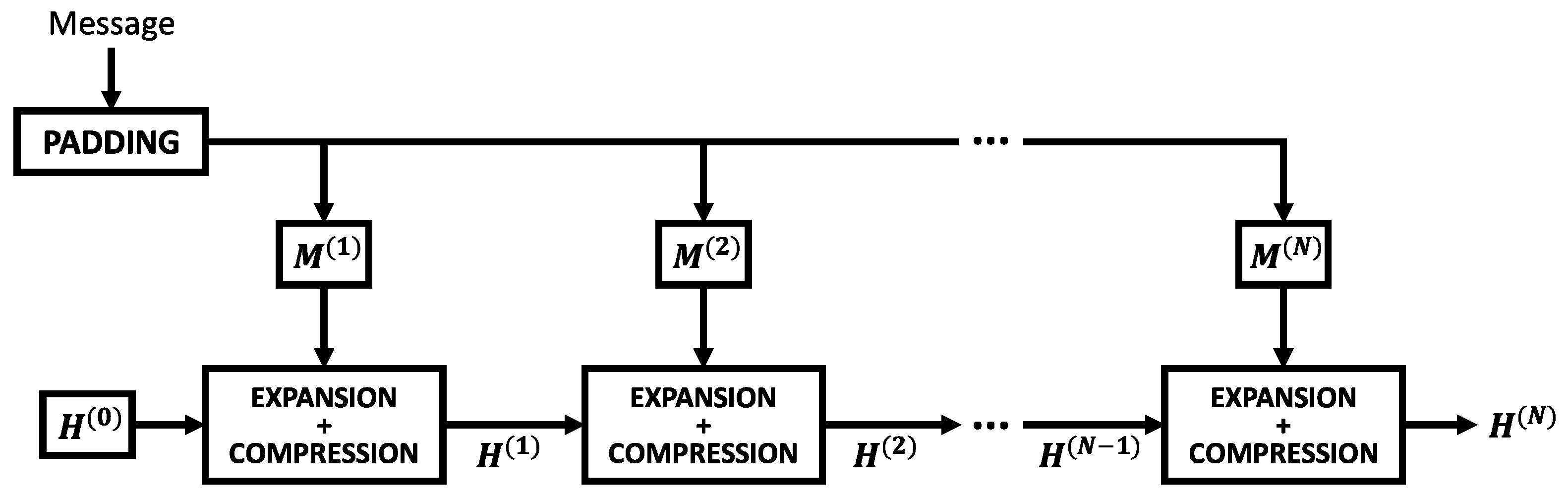
The SHA-256 algorithm takes an input message of up to bits and produces a fixed-length 256-bit output hash. The algorithm consists of two main stages: message preprocessing and hash computation. In the preprocessing stage, the input message is padded and divided into 512-bit blocks. In the hash computation stage, each block is expanded and compressed using a series of logical and arithmetic operations, resulting in a 256-bit message digest. The algorithm is designed to be resistant to various types of attacks, including collision attacks, where two different inputs produce the same output, and preimage attacks, where an attacker tries to find an input that produces a given output [3].
In the preprocessing stage, the input message is first encoded in the UTF-8 binary standard. Next, a 1-value bit is added to the end of the ℓ-length encoded input message as a delimiter, signaling the end of the binary sequence. Afterward, the delimited string is zero-padded to a length of k bits, and the original input message’s length ℓ is appended to the end in a 64-bit big-endian format. The value of k is determined as the smallest non-negative integer that satisfies the equation , where the notation means that A is an integer multiple of B. Then, the padded message is partitioned into a series of 512-bit blocks, denoted as , where i ranges from 1 to N. Each of these blocks comprises sixteen 32-bit words, represented as , with t ranging from 0 to 15 [3].
Finally, the last step of the preprocessing stage is initializing the working variables. These variables store the hash value and are refreshed each round of the algorithm. The symbols a, b, c, d, e, f, g, and h represent the working variables and are initialized with their respective values: , , …, , defined by the official documentation FIPS 180-4 Secure Hash Standard [3]. For subsequent message blocks ( 2, 3, …, N), the working variables are updated at the end of each block with the intermediate hash value . The updated working variables serve as initial values for the next message block until the final digest is computed. This design ensures that the hash is performed on the entire message rather than individual blocks. Figure 1 illustrates the overall SHA-256 workflow.
The hash computation stage starts by taking the 512-bit blocks generated in the preprocessing phase and feeding them into the expander module. This process expands the original sixteen 32-bit words into sixty-four 32-bit words denoted by . Table 2 shows the logical operators employed in the algorithm, while Algorithm 1 details the expansion operations.
| Algorithm 1: Expansion function. |
 |
The next stage of the SHA-256 algorithm involves computing the expanded message digest through 64 iterations of the compression function. This stage utilizes the state variables a, b, …, h, which were initialized during the preprocessing phase in conjunction with sixty-four 32-bit constants labeled as and defined by FIPS 180-4 [3]. Algorithm 2 exemplifies the steps of the compression function and its operators.
After 64 iterations, the intermediate hash for the respective block is computed as the sum of initialization hash with the final value stored in the state variables. This operation sequence is repeated for each message block ( 1, 2, …, N), and the final 256-bit message digest is obtained by concatenating the result hashes for , as illustrated in Algorithm 3. Table 3 presents two application examples of the SHA-256 algorithm provided by the official NIST publication [3]. Both input messages generate a 256-bit output hash (64 hexadecimal digits).
| Algorithm 2: Compression function. |
 |
| Algorithm 3: Block hashing. |
 |
3. Hardware Design
3.1. Digital ASIC Workflow
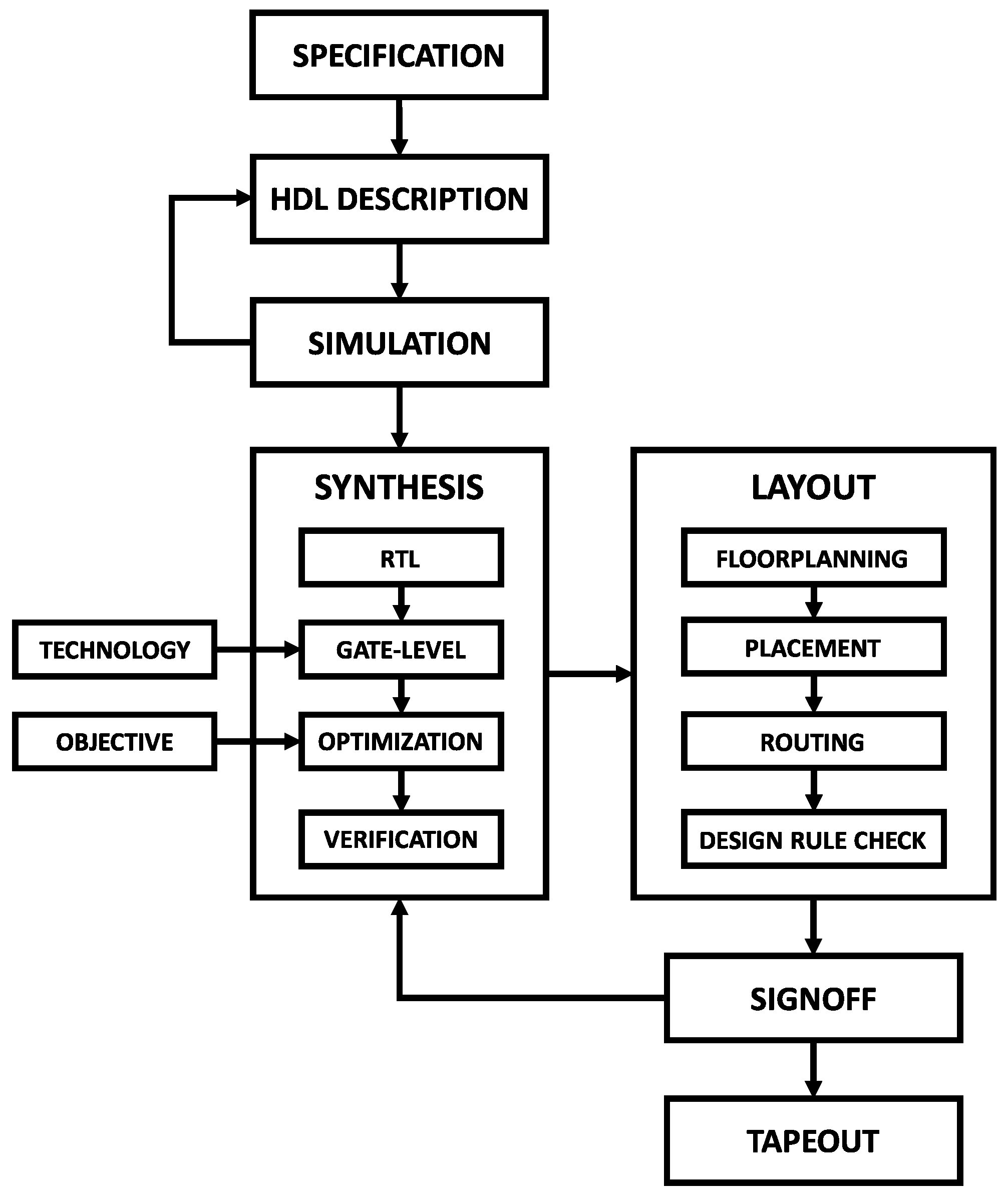
The typical digital ASIC design workflow, depicted in Figure 2, was adopted for the integrated circuit (IC) project. The first step consists of defining the electrical and functional aspects of the circuit that must be met during subsequent implementation stages. Next, an EDA-compatible hardware description language (HDL) is selected to describe the structure and behavior of the target digital circuit. The two most common HDLs are Verilog and VHDL, both of which are technology-independent. Once the design is coded in HDL, simulations must be conducted to check if the circuit meets the desired electrical and behavioral specifications [21]. The simulations may utilize test benches, which are automated test routines used to validate the created model functionality with a set of predefined control signals.
The synthesis phase begins with behavioral synthesis, where the high-level HDL design is “compiled” into a register-transfer level (RTL) description. During this process, the synthesis tool infers the logical structures required to match the system description. Afterward, the EDA tool executes logic synthesis, mapping the RTL blocks into standard logic cells and vendor-specific macros provided by the foundry through the process design kit (PDK). Multiple optimizations are made during the logic synthesis stage to enhance the final circuit’s speed, area, and power efficiency [22]. Verifications are performed at each stage to ensure the circuit’s consistency with the original description. The outcome of the synthesis phase is a netlist that describes the connections between hardware primitives [19].
The EDA tool utilizes the netlist generated during logical synthesis to create the integrated circuit layout. The physical design starts with the floorplanning stage, where the available core area is allocated among the main functional blocks, like logic elements, memory structures, and input–output interfaces. Then, the EDA tool proceeds to place and route (P&R) all standard logic cells and hardware macros according to the netlist description. After completing the P&R, the design rule checking (DRC) tool verifies if the final layout violates any of the PDK rules. Once all the previous steps are finished, the layout’s geometric files containing all the necessary information for the foundry to manufacture the integrated circuit are exported in GDSII format [22].
The signoff stage is the final verification step before the manufacturing phase, often referred to as “tapeout” [22]. During signoff, a series of analyses are performed on the final design, including layout versus schematic (LVS), voltage drop (IR drop) analysis, and static timing analysis (STA). LVS verifies the circuit’s integrity after component placement and routing, IR drop analysis assesses voltage level consistency across power lines, and STA evaluates circuit timing and the clock distribution network [19].
3.2. Open-Source EDA Tool and PDK
The open-source tool selected for the ASIC synthesis and layout design is the OpenLANE automated RTL to GDSII workflow [19]. This software routine utilizes custom scripts to bundle and automate the execution of a series of other open-source EDA tools, including OpenROAD [23], Yosys [24], Magic [25], Netgen [26], and KLayout [27]. OpenLANE takes a PDK and a Verilog design as inputs and generates the final GDSII files, along with a set of performance reports. The choice for the project’s PDK is the SkyWater SKY130 130 nm PDK [28], which was selected because of its open-source nature and seamless integration with OpenLANE. Additionally, SKY130 is currently the most advanced and tested open PDK available online, being one of the few open-source PDKs that an actual foundry can manufacture. All the codes and instructions for using OpenLANE are available on their GitHub page [29].
3.3. Hardware Architecture
The SHA-256 algorithm’s canonical form was implemented in Verilog HDL using a bottom–up approach. Since the project aimed to create an integrated circuit to work alongside a 32-bit microcontroller, the message padding and parsing stages were excluded from the ASIC design. Microcontrollers can efficiently handle these functions without significant computational overhead. However, the 64 iterations of expansion and compression of the SHA-256 algorithm are resource-intensive, so implementing these modules in hardware offers advantages, as it enhances performance and reduces CPU utilization.
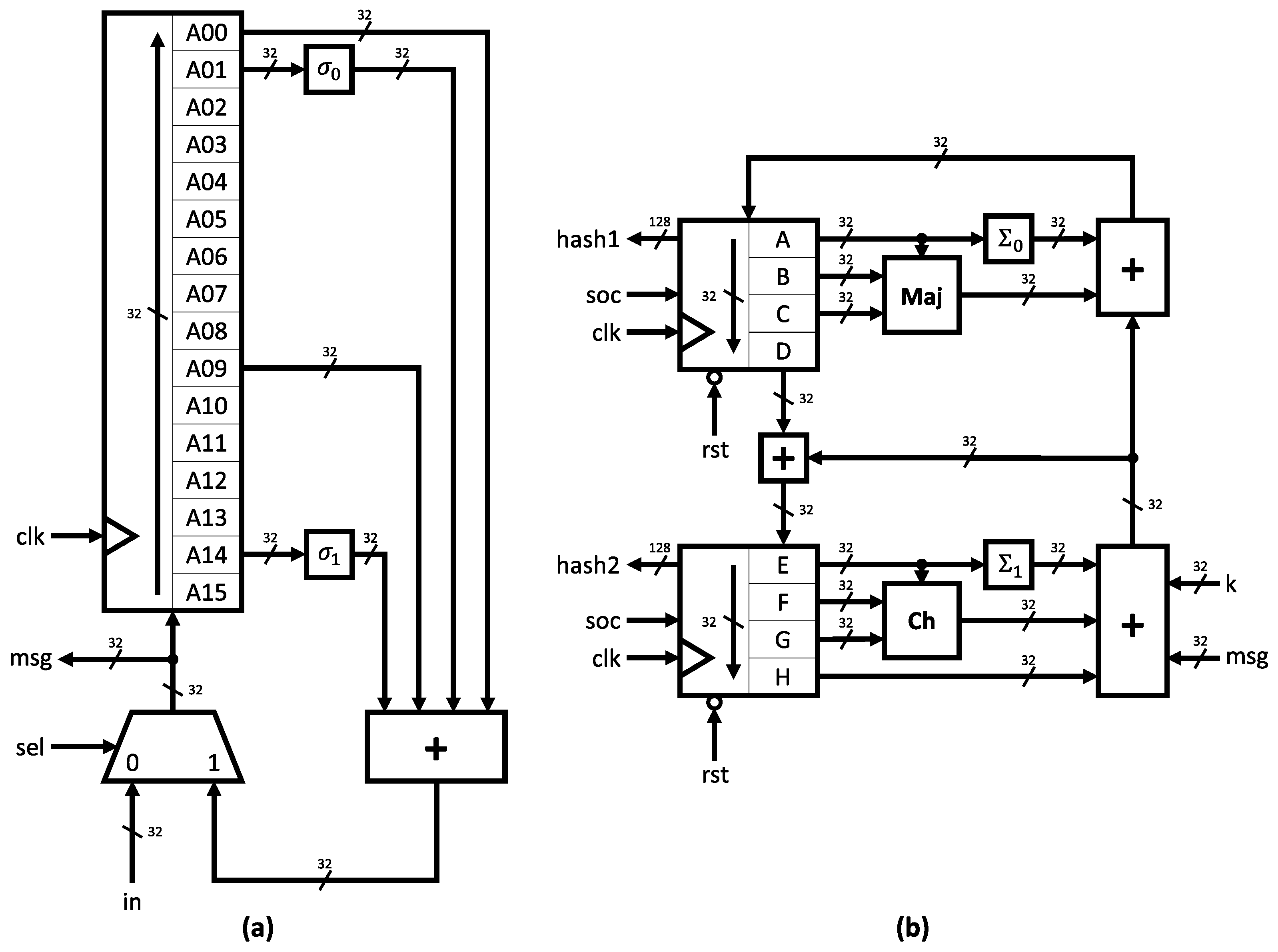
The message expander module is depicted in Figure 3a. The design consists of a 16-position 32-bit shift register and utilizes the operators described in Algorithm 1. Meanwhile, the message compressor module is shown in Figure 3b. This structure comprises state registers and the functions presented in Algorithm 2. All data-path widths are indicated in Figure 3, with unlabeled buses representing 1-bit signals. Both expander and compressor designs were coded in Verilog.
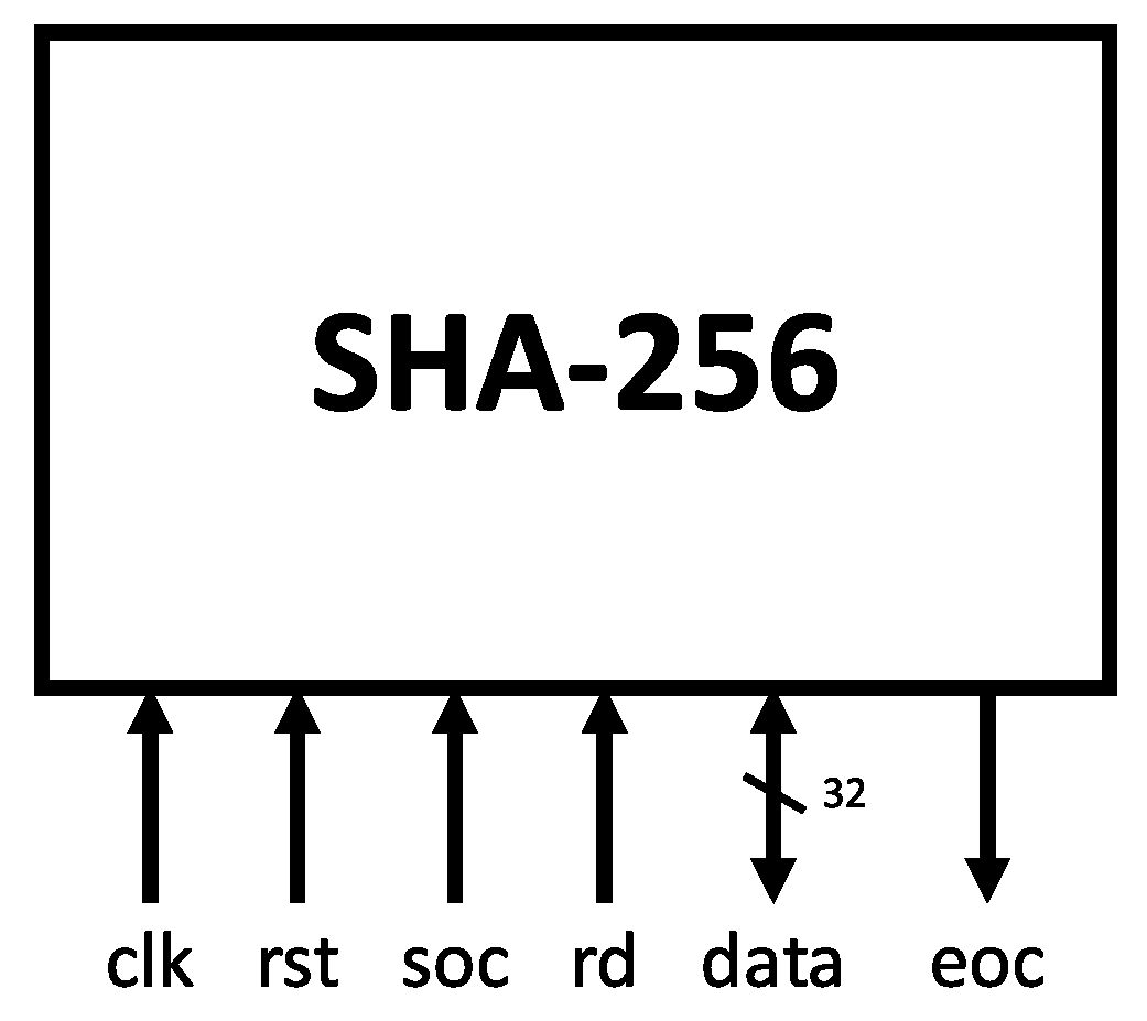
A 1-bit version of the compressor module state register is illustrated in Figure 4a. This logic structure is responsible for initializing the working variables, storing intermediate hashes, and generating the final output message digest. The proper operation of the algorithm depends not only on the main blocks but also on auxiliary modules. Figure 4b depicts the input–output interface, employing a 32-bit bidirectional bus for both input message and output hash. The constants used in the compression stage () are stored in an asynchronous 64 × 32 read-only memory (ROM). The ROM output is selected by the 6-bit address bus (addr).
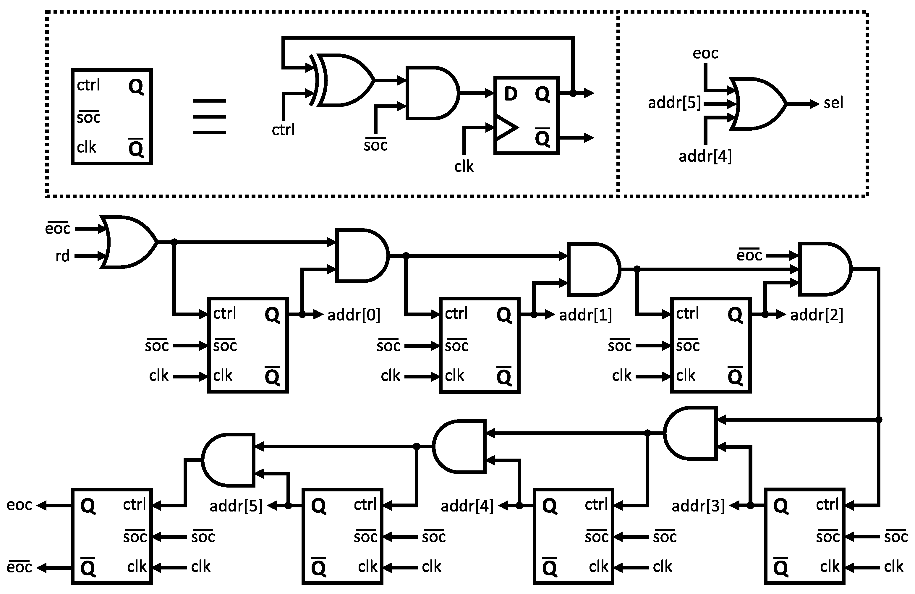
The final auxiliary module in the system is the 7-bit synchronous counter, as illustrated in Figure 5. This specific circuit plays a critical role in generating all ASIC internal control signals and ROM address signals required for the SHA-256 algorithm. It ensures proper synchronization across all stages, contributing to accurate and reliable system operation. Table 4 lists all control signals shown in Figure 3, Figure 4 and Figure 5 and their corresponding functions.
The top-level module of the SHA-256 algorithm implementation is presented in Figure 6. This description underwent extensive testing and validation using official data from NIST [3] and other online hash examples [30]. A flexible testbench was developed to facilitate verification across multiple test cases involving messages from single and multiple blocks. The final design version exhibited correct behavior throughout all test samples.
3.4. Design Control Sequence
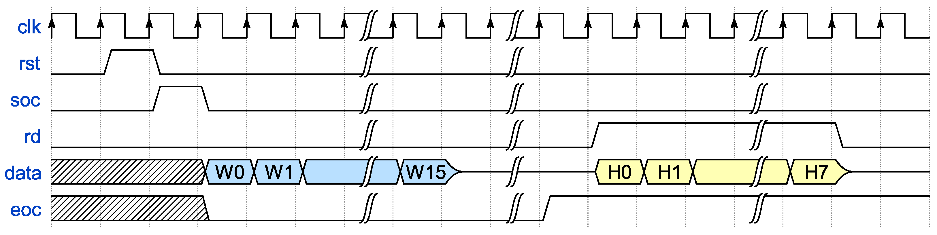
Figure 7 depicts the sequence of control signals required for computing and reading the hash result of a single-block message. The values W0, W1, …, W15 represent the message data, while H0, H1, …, H7 denote the 32-bit chunks of the resulting 256-bit hash value. Leaving the rd signal active after completing a reading cycle causes the system to re-output the message digest (displaying H0 to H7).
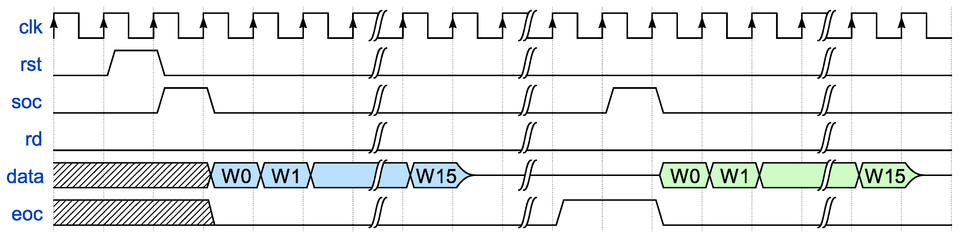
Figure 8 illustrates the control sequence required for computing the hash of a multi-block message. In this particular example, the reading process is not depicted. However, it should be executed similarly to the previous example, following the end-of-computation (eoc) signal after the last message block. In this second timing diagram, the first message block is represented in blue, while the second is depicted in green.
4. Results and Discussion
4.1. Performance Metrics
To objectively evaluate ASIC designs, it is crucial to define performance metrics to remove subjective factors from the analysis. In line with the related work presented in Section 1, the total core area and the maximum operating frequency were selected as the primary evaluation criteria. Typically, circuit speed and layout area exhibit an inverse correlation, meaning that the optimal design may not yield the best results in both metrics simultaneously. Therefore, a circuit is considered above average if it demonstrates a higher frequency/area ratio when compared to other designs. For the SHA-256 ASIC, a higher clock frequency implies more hashes per second, while a smaller area enables its application on embedded devices or high-density cryptographic accelerators.
4.2. Synthesis Results
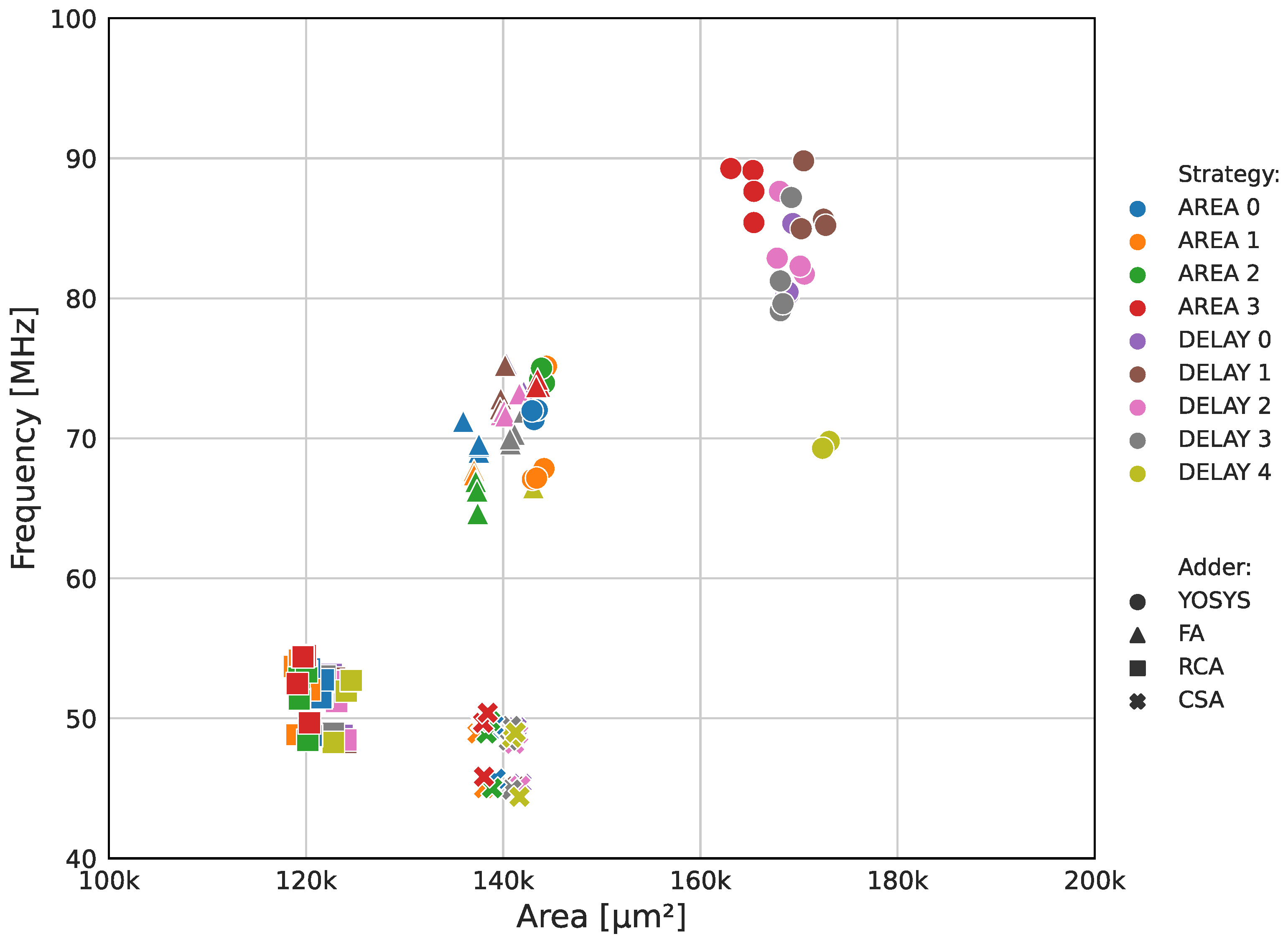
The OpenLANE EDA tool offers over 250 configuration parameters to configure the project workflow. According to their official documentation [31], the two critical parameters for enhancing circuit speed and reducing area are the adder topology and the synthesis strategy. There are four adder structures available: full-adder (FA), ripple carry adder (RCA), carry select adder (CSA), and Yosys’ internal adder definition (YOSYS). The synthesis strategy offers nine options grouped into two main classes: area optimization (AREA, with four levels) and delay optimization (DELAY, with five levels). An initial exploratory study was conducted on these variables to evaluate the impact of each parameter on the final circuit’s performance, as depicted in Figure 9. During this analysis, the target clock period was varied from 10 ns to 50 ns in 10 ns increments, resulting in a total of 180 tested combinations. The remaining flow parameters were set to their default values, per the documentation [31]. Each flow took approximately 30 min to complete. Not all flows were successful, so they are not plotted on the graph.
Figure 9 provides enough data to conclude that the adder topology variable has the most impact on the circuit speed and area compared to the other tested parameters. The YOSYS architecture presented the best frequency results, while the RCA resulted in the smallest cores. This preliminary analysis also shows the already-mentioned inverse relation between maximum frequency and device area. Increasing speed demands a restructuring of the circuit’s critical path, which requires parallelizing functions and logic structures, consequently adding more cells.
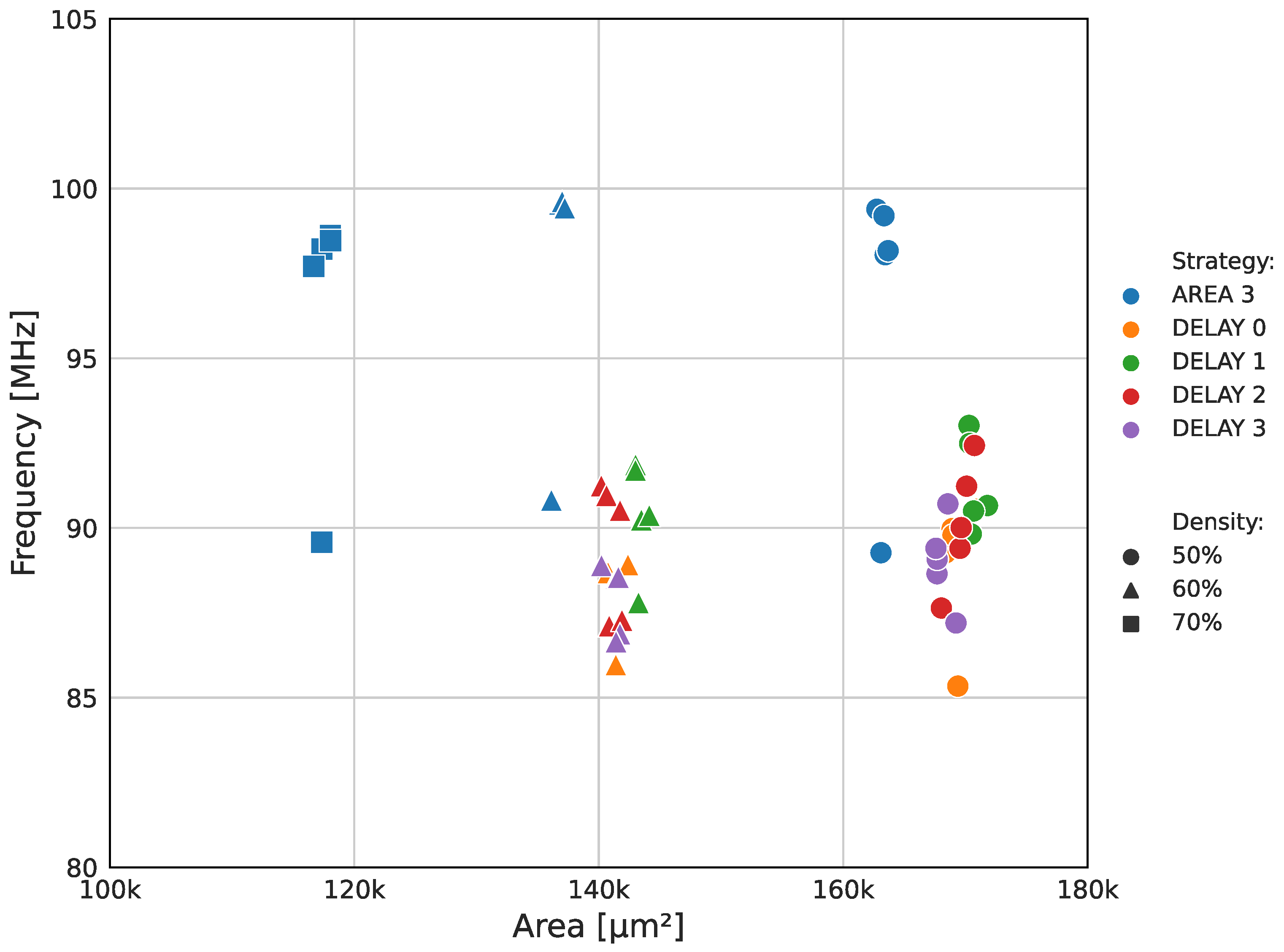
Regarding the synthesis strategy parameter, Figure 9 shows that this variable plays a smaller role than the adder topology, but it is still a key factor in achieving higher-speed designs. Among the available options, AREA 3, DELAY 0, DELAY 1, DELAY 2, and DELAY 3 performed the best frequency-wise. The target clock period parameter had a minor impact on the circuit performance, resulting in marginal variations of up to 5% in both area and frequency. This outcome is attributed to the fact that the target clock period mainly affects the layout stage, acting as a goal for the P&R tool to optimize cell positioning and minimize parasitic capacitances.
A second exploratory analysis was conducted to maximize the circuit speed and minimize the ASIC area. The results are presented in Figure 10. The second study focused on reducing the size of the high-speed designs rather than increasing the maximum frequency of the slower ones. This approach was selected because of the inherent dependence between maximum frequency and the logical structure, primarily determined during the logical synthesis phase. The target area density parameter was increased from the default 50% up to 90% in 10% steps to force the P&R tool to optimize the cell positioning and routing to obtain a layout with reduced core area. The density variable informs the total core area used by logic cells, with 100% density being unfeasible because of the lack of space required for routing. Similar to the previous study, the target clock period was varied within the 10 ns to 20 ns interval in 2 ns steps to search for the optimal flow configuration. All designs with a target density above 70% failed, indicating a layout area constraint. Only the successful flow results are plotted in the graph.
The second exploratory analysis identified the AREA 3 configuration as the optimal synthesis strategy for high-speed, high-density designs. This setting enabled layouts with a cell density of up to 70%, resulting in smaller ASIC cores without sacrificing speed. The circuit with the best frequency/area ratio in Figure 10 presents a maximum operating frequency of 97.7 MHz and a core area of 116,665 µm2. This layout outperformed all designs found in the first exploratory study in terms of both operating frequency and core area.
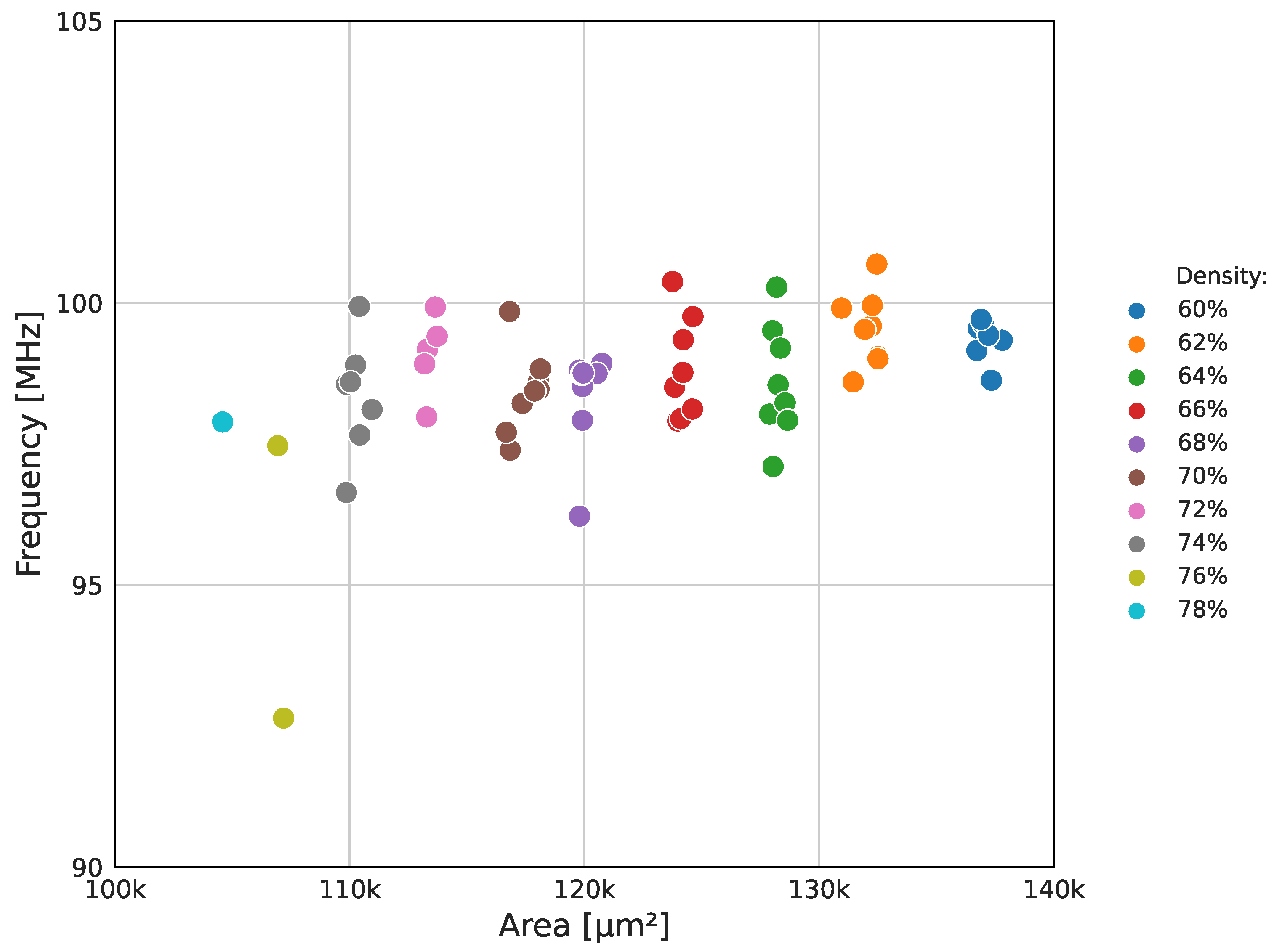
Once the optimal combination of synthesis strategy and adder topology (AREA 3 and YOSYS) was identified, a local search was conducted to find the ASIC design with the best frequency/area ratio. The results are shown in Figure 11. The target clock period and density parameters were finely swept across 10 ns to 20 ns and 60% to 80%, respectively. These ranges were defined based on the constraints identified in the previous exploratory studies. All other OpenLANE control variables remained unaltered, maintaining their default values as provided in the documentation [31]. The graph only displays the successful flow results.
The local search yielded several designs with better frequency/area ratios compared to previous workflows. Figure 11 illustrates the impact of the target density on the layout area, reducing the ASIC size by 25% from 137,796 µm2 (worst density result of 60%) to 104,585 µm2 (density result of 78%). This significant reduction caused a minor decrease of 2% in the maximum clock frequency, highlighting the critical path’s dependence on the logic synthesis phase. The results displayed a 3% average frequency variation attributed to the target clock period parameter. No additional investigations were conducted because of the already-evaluated design limitations.
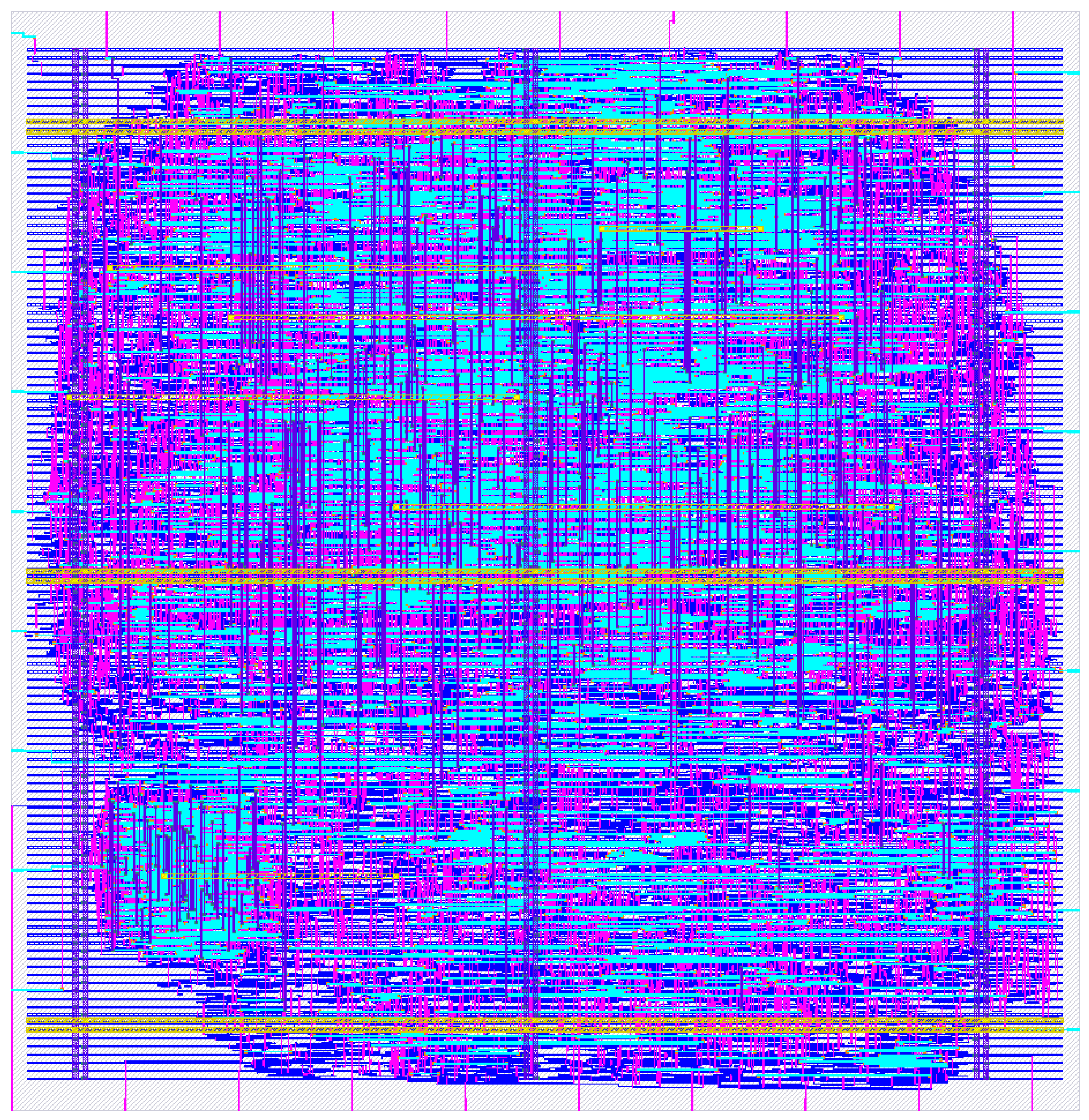
4.3. Final Layout
The final SHA-256 cryptographic hardware accelerator ASIC design is shown in Figure 12. This layout presented the best frequency/area ratio among all flows, and was generated with the following OpenLANE EDA configurations: AREA 3 synthesis strategy, YOSYS adder topology, 13 ns target clock period, and 78% target core density. All remaining parameters were set to their default values as provided in the documentation [31]. The estimated performance metrics of the IC and comparison data are compiled in Table 5. The ASIC core area is presented in both square microns and gate equivalent (GE), which measures design complexity by dividing the layout area by the area of a two-input NAND gate implemented in the same process node. This technology-independent metric offers a direct way for comparing circuits synthesized in different PDKs [16]. The ASIC design successfully passed all OpenLANE verifications, including LVS, IR drop analysis, and STA.
Comparing ASIC designs implemented in different silicon nodes based on technology-dependent metrics is often unfair and provides little to no useful information. Newer manufacturing processes offer substantial advantages in terms of speed, area, and power efficiency when compared to older ones. Therefore, the gate equivalent count is the only valid comparison metric available, as it yields a technology-normalized circuit complexity unit. A larger GE implies that the ASIC uses more standard cells in its design, making it more complex.
When compared to other publications (as presented in Section 1), the GE count reveals that the proposed ASIC exhibits the lowest complexity among Xu et al. [10] and Nannipieri et al. [16] designs. This outcome was already expected, as the developed circuit employs the canonical structure of the SHA-256 algorithm, which lacks optimization techniques like pipelining and critical path restructuring. This architectural decision was made to maintain the final device as simple as possible, making it an easy-to-use macro for future integration into 32-bit microcontroller designs where a small-area SHA-256 hash engine is needed.
5. Conclusions
The final SHA-256 ASIC design implemented in SkyWater SKY130 130 nm process technology exhibited a small area and decent maximum operating frequency, being suited for 32-bit microcontrollers. All project steps were developed using only open-source EDA tools to make the final design as easy to reproduce as possible. The Verilog HDL description files, as well as other supporting materials, can be found on the project’s GitHub page.
Future work can be done to improve the SHA-256 hardware accelerator design with parallel structures and pipelining techniques to reduce the critical path and allow the simultaneous calculation of multiple hashes. In addition, similar cryptographic algorithms can be incorporated into the design, creating a hybrid structure that reduces the required hardware to perform multiple functions.
Author Contributions
Conceptualization, L.D.F. and M.L.; Methodology, L.D.F.; Investigation, L.D.F.; Software, L.D.F.; Validation, G.A.G. and J.P.C.; Resources, J.A.A.; Writing—original draft preparation, L.D.F.; Writing—review and editing, G.A.G., J.P.C. and J.A.A.; Supervision, M.L.; Funding acquisition, M.L. All authors have read and agreed to the published version of the manuscript.
Funding
This research was funded by Brazil’s National Council for Scientific and Technological Development (CNPq) grant number 120527/2022-7.
Data Availability Statement
The data presented in this study, including hardware description, exploratory analysis results, and auxiliary OpenLANE scripts, are openly available on the project’s GitHub page [20].
Conflicts of Interest
The authors declare no conflicts of interest. The funders had no role in the design of the study; in the collection, analyses, or interpretation of data; in the writing of the manuscript; or in the decision to publish the results.
Abbreviations
The following abbreviations are used in this manuscript:
| ASIC | Application-Specific Integrated Circuit |
| CMOS | Complementary Metal-Oxide Semiconductor |
| CPU | Central Processing Unit |
| CSA | Carry-Save Adder |
| DRC | Design Rule Checking |
| EDA | Electronic Design Automation |
| FA | Full Adder |
| FPGA | Field-Programmable Gate Arrays |
| GE | Gate Equivalent |
| HDL | Hardware Description Language |
| IC | Integrated Circuit |
| IR | Voltage |
| IoT | Internet of Things |
| LVS | Layout Versus Schematic |
| NIST | National Institute of Standards and Technology |
| NSA | National Security Agency |
| P&R | Place and Route |
| PDK | Process Design Kit |
| RCA | Ripple-Carry Adder |
| ROM | Read-Only Memory |
| RTL | Register Transfer Level |
| SHA | Secure Hash Algorithm |
| SMIC | Semiconductor Manufacturing International Corporation |
| STA | Static Timing Analysis |
| TSMC | Taiwan Semiconductor Manufacturing Company |
| VHDL | VHSIC Hardware Description Language |
| VHSIC | Very High Speed Integrated Circuit |
References
- Andrews, W.; Lindeman, T. The Black Budget. The Washington Post. 29 August 2013. Available online: https://www.washingtonpost.com/wp-srv/special/national/black-budget/ (accessed on 23 February 2023).
- Rawal, B.S.; Kumar, L.S.; Maganti, S.; Godha, V. Comparative Study of Sha-256 Optimization Techniques. In Proceedings of the 2022 IEEE World AI IoT Congress (AIIoT), Seattle, WA, USA, 6–9 June 2022; pp. 387–392. [Google Scholar]
- FIPS 180-4; Secure Hash Standard (SHS). Federal Information Processing Standards Publication, National Institute of Standards and Technology: Gaithersburg, MD, USA, August 2015.
- Zhang, X.; Liu, B.; Zhao, Y.; Hu, X.; Shen, Z.; Zheng, Z.; Liu, Z.; Chong, K.-S.; Yu, G.; Wang, C.; et al. Design and Analysis of Area and Energy Efficient Reconfigurable Cryptographic Accelerator for Securing IoT Devices. Sensors 2022, 22, 9160. [Google Scholar] [CrossRef] [PubMed]
- Sghaier, A.; Zeghid, M.; Massoud, C.; Mahchout, M. Design And Implementation of Low Area/Power Elliptic Curve Digital Signature Hardware Core. Electronics 2017, 6, 46. [Google Scholar] [CrossRef]
- Diehl, W.; Abdulgadir, A.; Kaps, J.-P.; Gaj, K. Comparing the Cost of Protecting Selected Lightweight Block Ciphers against Differential Power Analysis in Low-Cost FPGAs. Computers 2018, 7, 28. [Google Scholar] [CrossRef]
- Nam, H.; Lysecky, R. Mixed Cryptography Constrained Optimization for Heterogeneous, Multicore, and Distributed Embedded Systems. Computers 2018, 7, 29. [Google Scholar] [CrossRef]
- Baldanzi, L.; Crocetti, L.; Falaschi, F.; Bertolucci, M.; Belli, J.; Fanucci, L.; Saponara, S. Cryptographically Secure Pseudo-Random Number Generator IP-Core Based on SHA2 Algorithm. Sensors 2020, 20, 1869. [Google Scholar] [CrossRef] [PubMed]
- Zhu, S.; Zhu, C.; Wang, W. A New Image Encryption Algorithm Based on Chaos and Secure Hash SHA-256. Entropy 2018, 20, 716. [Google Scholar] [CrossRef] [PubMed]
- Xu, W.; Xu, Y.; Huo, G.; Yang, Y.; Jin, Y. Optimized Dual-mode Security Encryption Chip Design Based on Hash Algorithm. In Proceedings of the 2022 IEEE 11th International Conference on Communication Systems and Network Technologies (CSNT), Indore, India, 23–24 April 2022; pp. 566–570. [Google Scholar]
- Dadda, L.; Macchetti, M.; Owen, J. The design of a high speed ASIC unit for the hash function SHA-256 (384, 512). In Proceedings of the Design, Automation and Test in Europe Conference and Exhibition, Paris, France, 16–20 February 2004; Volume 3, pp. 70–75. [Google Scholar]
- Bai, L.; Li, S. VLSI implementation of high-speed SHA-256. In Proceedings of the 2009 IEEE 8th International Conference on ASIC, Changsha, China, 20–23 October 2009; pp. 131–134. [Google Scholar]
- Wu, R.; Zhang, X.; Wang, M.; Wang, L. A High-Performance Parallel Hardware Architecture of SHA-256 Hash in ASIC. In Proceedings of the 2020 22nd International Conference on Advanced Communication Technology (ICACT), Phoenix Park, Republic of Korea, 16–19 February 2020; pp. 1242–1247. [Google Scholar]
- Li, J.; He, Z.; Qin, Y. Design of Asynchronous High Throughput SHA-256 Hardware Accelerator in 40nm CMOS. In Proceedings of the 2019 IEEE 13th International Conference on ASIC (ASICON), Chongqing, China, 30 October–1 November 2019; pp. 1–4. [Google Scholar]
- Zhang, Y.; He, Z.; Wan, M.; Zhan, M.; Zhang, M.; Peng, K.; Song, M.; Gu, H. A New Message Expansion Structure for Full Pipeline SHA-2. IEEE Trans. Circuits Syst. Regul. Pap. 2021, 68, 1553–1566. [Google Scholar] [CrossRef]
- Nannipieri, P.; Bertolucci, M.; Baldanzi, L.; Crocetti, L.; Di Matteo, S.; Falaschi, F.; Fanucci, L.; Saponara, S. SHA2 and SHA-3 accelerator design in a 7 nm technology within the European Processor Initiative. Microprocess Microsyst. 2020, 87, 103444. [Google Scholar] [CrossRef]
- Le, V.T.D.; Pham, H.L.; Duong, T.S.; Tran, T.H.; Nguyen, Q.D.N.; Nakashima, Y. RHCP: A Reconfigurable High-efficient Cryptographic Processor for Decentralized IoT Platforms. In Proceedings of the 2023 15th International Conference on Knowledge and Systems Engineering (KSE), Hanoi, Vietnam, 18–20 October 2023; pp. 1–6. [Google Scholar]
- Michail, H.E.; Athanasiou, G.S.; Theodoridis, G.; Gregoriades, A.; Goutis, C.E. Design and implementation of totally-self checking SHA-1 and SHA-256 hash functions’ architectures. Microprocess Microsyst. 2016, 45, 227–240. [Google Scholar] [CrossRef]
- Shalan, M.; Edwards, T. Building OpenLANE: A 130nm OpenROAD-based Tapeout- Proven Flow: Invited Paper. In Proceedings of the 2020 IEEE/ACM International Conference On Computer Aided Design (ICCAD), San Diego, CA, USA, 2–5 November 2020; pp. 1–6. [Google Scholar]
- LDFranck. Custom ASIC Design for SHA-256 GitHub. 2023. Available online: https://github.com/LDFranck/SHA-256 (accessed on 1 November 2023).
- D’Amore, R. VHDL Descrição e Síntese de Circuitos Digitais, 2nd ed.; LTC: Rio de Janeiro, Brazil, 2005; p. 308. [Google Scholar]
- Balaji, S. Digital Design Flow Techniques and Circuit Design for Thin-Film Transistors. Master’s Thesis, Lund University, Lund, Sweden, 18 June 2020. [Google Scholar]
- The OpenROAD Project. Available online: https://theopenroadproject.org/ (accessed on 1 November 2023).
- YosysHQ. Yosys Open Synthesis Suite GitHub. 2023. Available online: https://github.com/YosysHQ/yosys (accessed on 1 November 2023).
- RTimothyEdwards. Magic GitHub. 2023. Available online: https://github.com/RTimothyEdwards/magic (accessed on 1 November 2023).
- RTimothyEdwards. Netgen GitHub. 2023. Available online: https://github.com/RTimothyEdwards/netgen (accessed on 1 November 2023).
- KLayout EDA Tool. Available online: https://www.klayout.de/ (accessed on 1 November 2023).
- SkyWater Foundries. FOSS 130 nm Production PDK. 2020. Available online: https://skywater-pdk.readthedocs.io/ (accessed on 6 August 2023).
- Efabless Corporation. OpenLANE Project GitHub. 2023. Available online: https://github.com/The-OpenROAD-Project/OpenLane (accessed on 6 August 2023).
- Martin, D. SHA-256 Algorithm Explained. 2022. Available online: https://sha256algorithm.com/ (accessed on 2 March 2023).
- Efabless Corporation. The OpenLANE Documentation. 2022. Available online: https://openlane.readthedocs.io/ (accessed on 6 August 2023).
Figure 1.
Block diagram of SHA-256 workflow.

Figure 2.
Digital ASIC design workflow.

Figure 3.
(a) Expander module. (b) Compressor module.

Figure 4.
(a) One-bit state register. (b) Input–output interface.

Figure 5.
Synchronous counter.

Figure 6.
SHA-256 top-level module.

Figure 7.
Single-block message timing diagram.

Figure 8.
Multiple-block message timing diagram.

Figure 9.
Results of the first exploratory study. Target clock period variations are represented by markers with the same shape and color.
Figure 9.
Results of the first exploratory study. Target clock period variations are represented by markers with the same shape and color.

Figure 10.
Results of the second exploratory study. Target clock period variations are represented by markers with the same shape and color. All designs were synthesized with YOSYS adder topology.
Figure 10.
Results of the second exploratory study. Target clock period variations are represented by markers with the same shape and color. All designs were synthesized with YOSYS adder topology.

Figure 11.
Results of the local search. Target clock period variations are represented by markers with the same color. All designs were synthesized with YOSYS adder topology and AREA 3 strategy.
Figure 11.
Results of the local search. Target clock period variations are represented by markers with the same color. All designs were synthesized with YOSYS adder topology and AREA 3 strategy.

Figure 12.
Final SHA-256 ASIC layout.


Table 1.
Related work comparison.
| Design | Year | Technology | Frequency (MHz) | Area | Cycles * | Power (mW) | |
|---|---|---|---|---|---|---|---|
| (µm2) | GE | ||||||
| [10] | 2022 | SMIC 65 nm | 472 | - | 35,600 | - | 4.97 |
| [11] | 2004 | ST 180 nm | 819 | 164,856 | - | 67 | - |
| [12] | 2009 | SMIC 180 nm | 208 | 211,955 | - | 65 | - |
| [13] | 2019 | Intel 14 nm | 1530 | 14,273 | - | - | 6.86 |
| [14] | 2019 | SMIC 40 nm | 227 | 38,885 | - | 32 | - |
| [15] | 2021 | 28 nm CMOS | 446 | 209,773 | - | 1 | 252 |
| [16] | 2021 | TSMC 7 nm | 5150 | - | 31,550 | 67 | 13.5 |
| [17] | 2023 | FreePDK 45 nm | 254 | - | - | 16 | 1850 |
| [18] | 2016 | TSMC 90 nm | 503 | 209,624 | - | 8 | 128 |
* Number of clock cycles per message block.
Table 2.
SHA-256 logical operators.
| Symbol | Operation |
|---|---|
| ∧ | Bitwise AND |
| ∨ | Bitwise OR |
| ⊕ | Bitwise XOR |
| ¬ | Bitwise NOT |
| + | Addition modulo |
| Concatenation | |
| Right-shift by n bits | |
| Rotate-right by n bits |
Table 3.
SHA-256 examples.
| Input Message | Hexadecimal Hash |
|---|---|
| abc | BA7816BF 8F01CFEA 414140DE 5DAE2223 B00361A3 96177A9C B410FF61 F20015AD |
| abcdbcdecdefdefgefghfghighij hijkijkljklmklmnlmnomnopnopq | 248D6A61 D20638B8 E5C02693 0C3E6039 A33CE459 64FF2167 F6ECEDD4 19DB06C1 |
Table 4.
ASIC control signals.
| Signal | Function |
|---|---|
| clk | Clock signal |
| sel | Data selection |
| in | External data input |
| msg | Expander module output |
| soc | Start of computation |
| eoc | End of computation |
| rst | Master reset |
| k | Constants () |
| hash1+hash2 | Hash output |
Disclaimer/Publisher’s Note: The statements, opinions and data contained in all publications are solely those of the individual author(s) and contributor(s) and not of MDPI and/or the editor(s). MDPI and/or the editor(s) disclaim responsibility for any injury to people or property resulting from any ideas, methods, instructions or products referred to in the content. |
© 2023 by the authors. Licensee MDPI, Basel, Switzerland. This article is an open access article distributed under the terms and conditions of the Creative Commons Attribution (CC BY) license (https://creativecommons.org/licenses/by/4.0/).
Share and Cite
MDPI and ACS Style
Franck, L.D.; Ginja, G.A.; Carmo, J.P.; Afonso, J.A.; Luppe, M. Custom ASIC Design for SHA-256 Using Open-Source Tools. Computers 2024, 13, 9. https://doi.org/10.3390/computers13010009
AMA Style
Franck LD, Ginja GA, Carmo JP, Afonso JA, Luppe M. Custom ASIC Design for SHA-256 Using Open-Source Tools. Computers. 2024; 13(1):9. https://doi.org/10.3390/computers13010009
Chicago/Turabian StyleFranck, Lucas Daudt, Gabriel Augusto Ginja, João Paulo Carmo, José A. Afonso, and Maximiliam Luppe. 2024. "Custom ASIC Design for SHA-256 Using Open-Source Tools" Computers 13, no. 1: 9. https://doi.org/10.3390/computers13010009
Note that from the first issue of 2016, this journal uses article numbers instead of page numbers. See further details here.