Comparison of the Physicochemical Properties of TiO2 Thin Films Obtained by Magnetron Sputtering with Continuous and Pulsed Gas Flow

 , , ,
, , ,
Abstract
:1. Introduction
2. Materials and Methods
3. Results
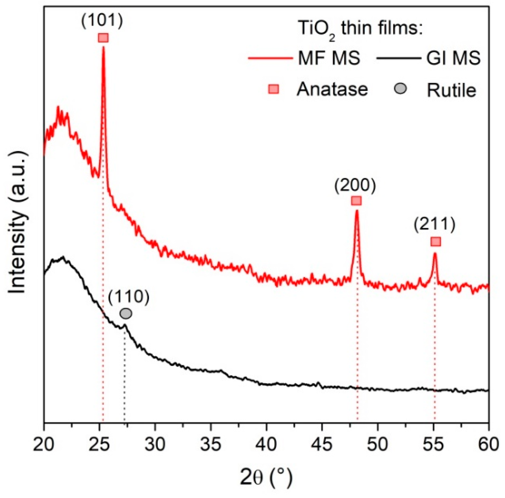
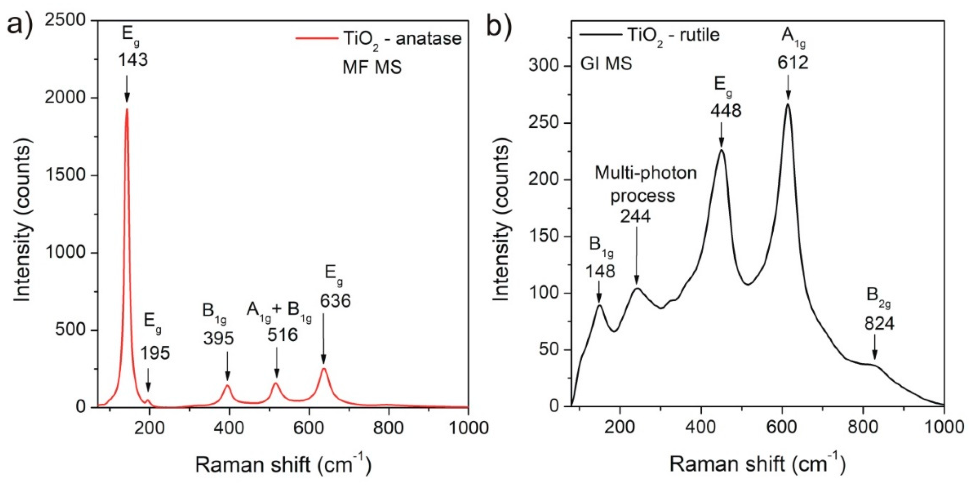
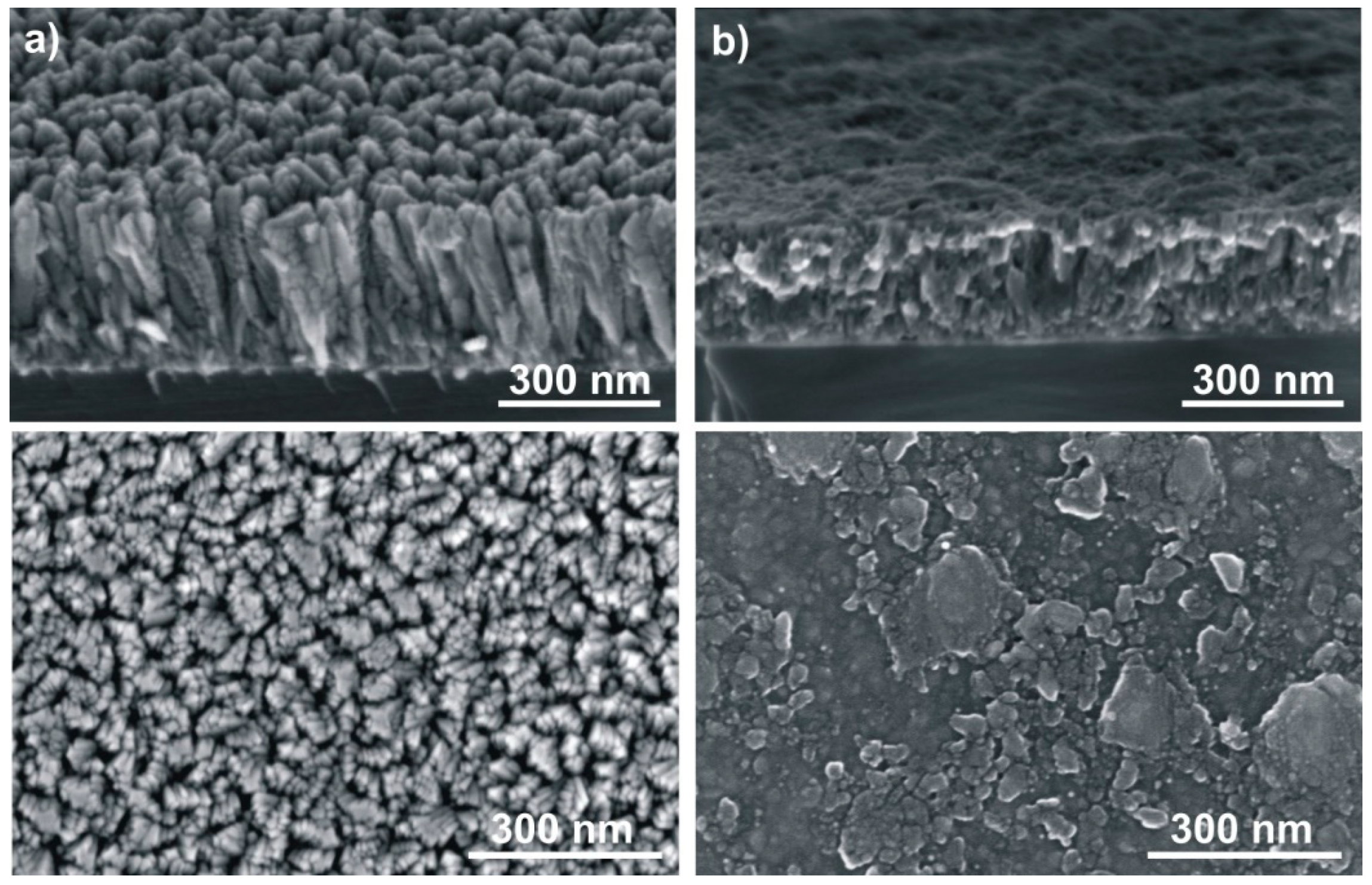
3.1. Microstructure
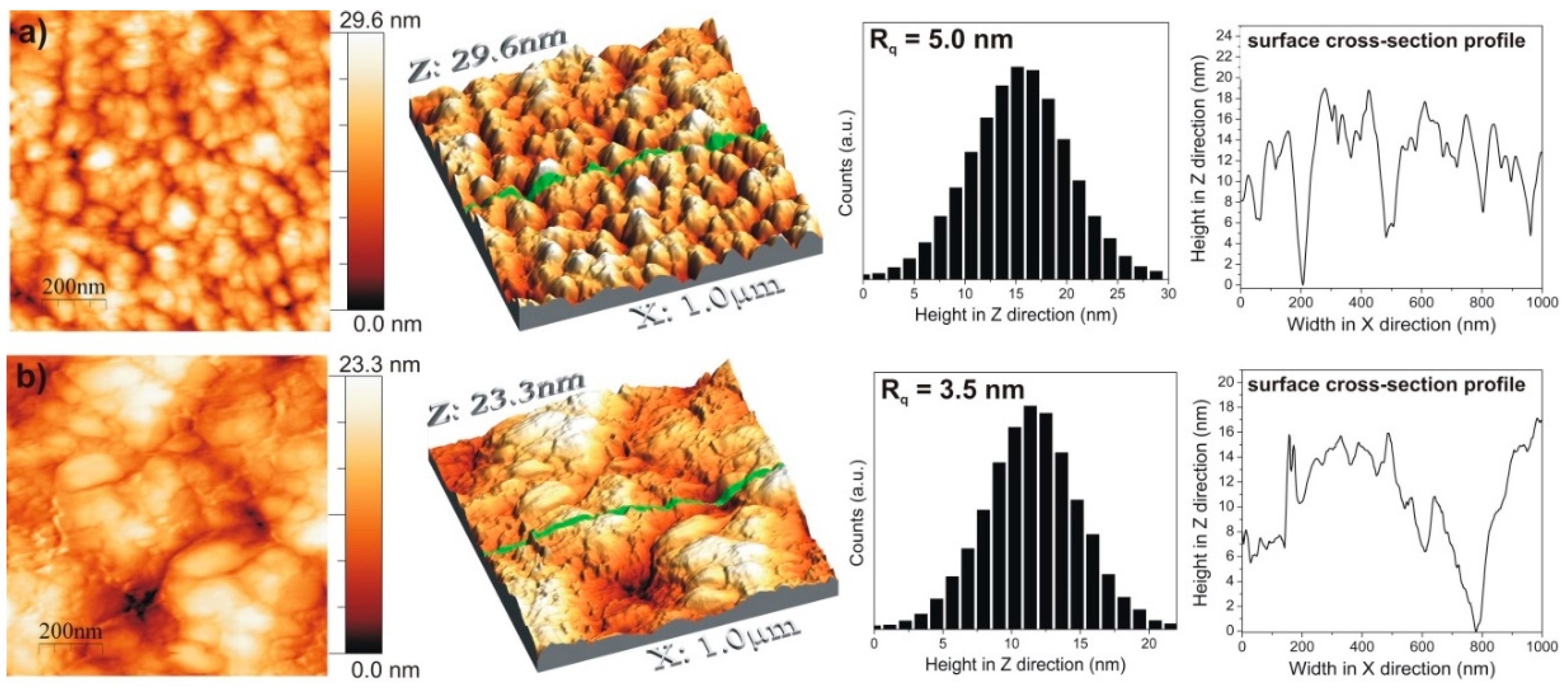
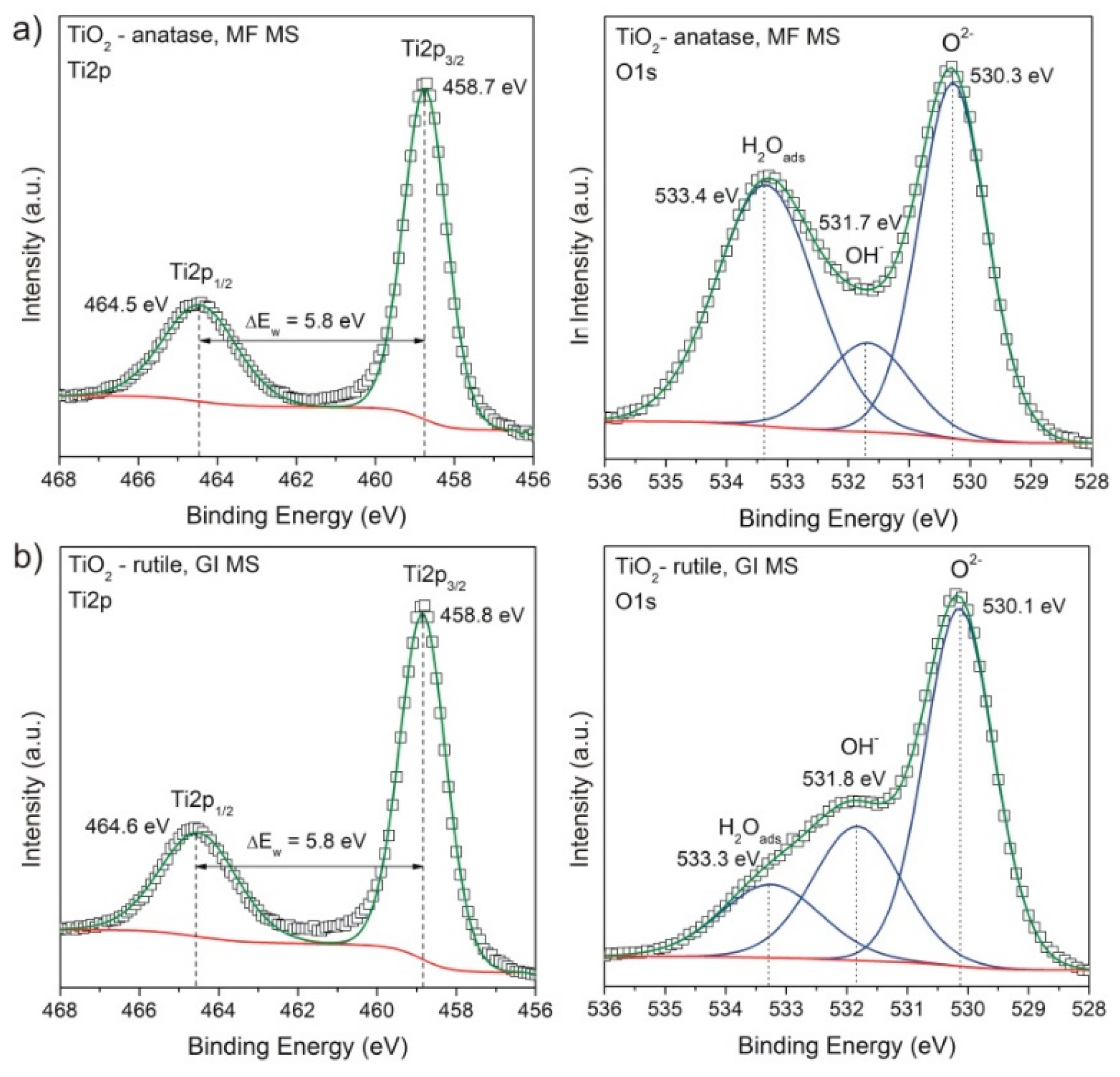
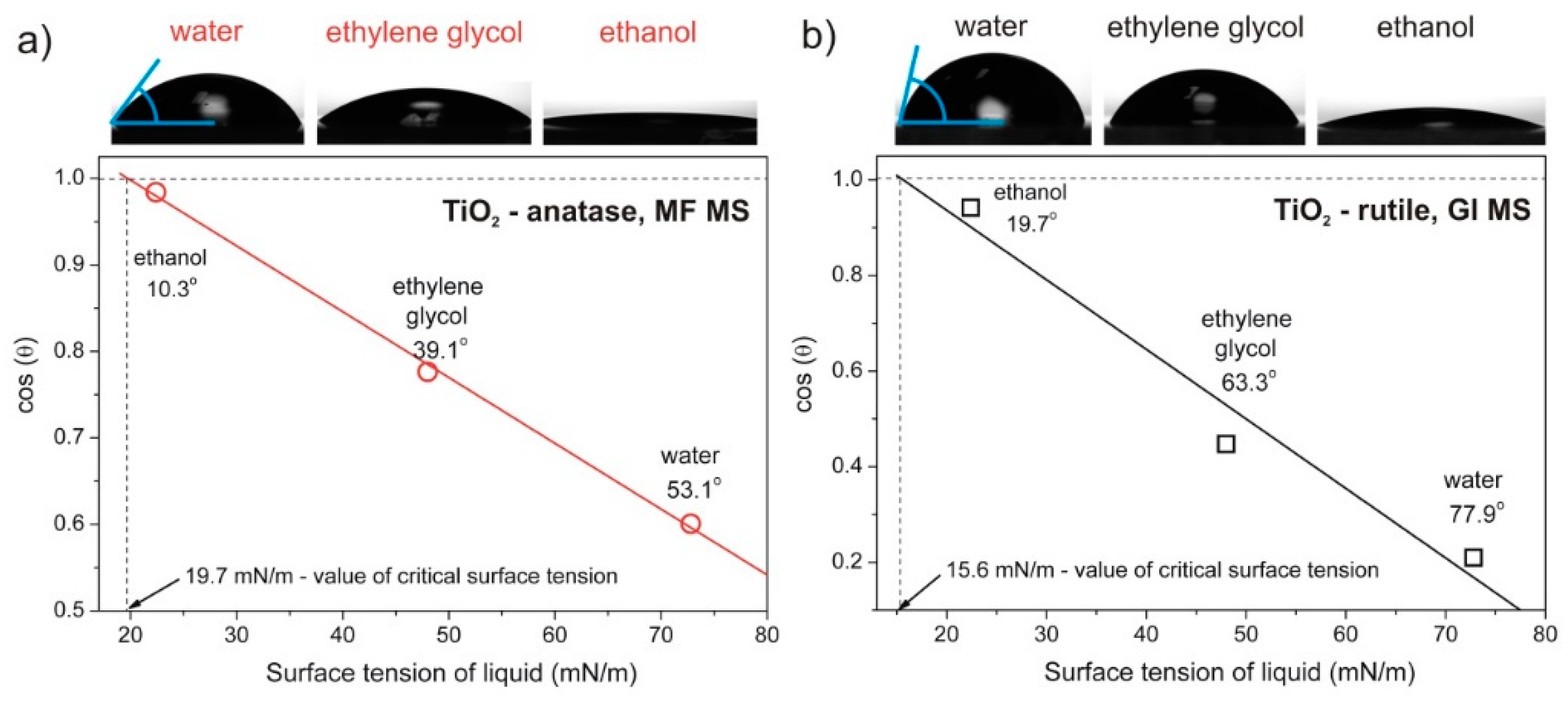
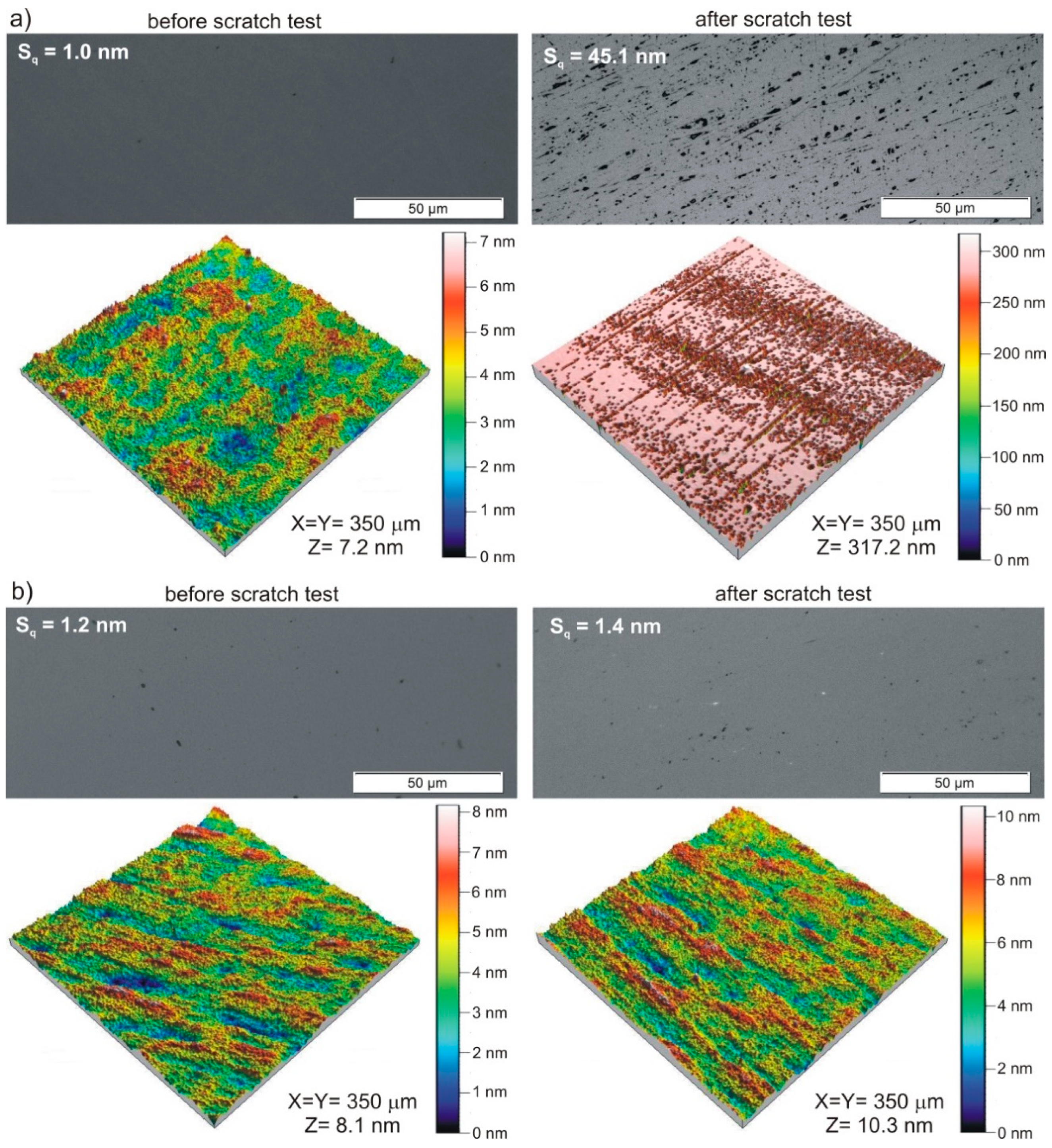
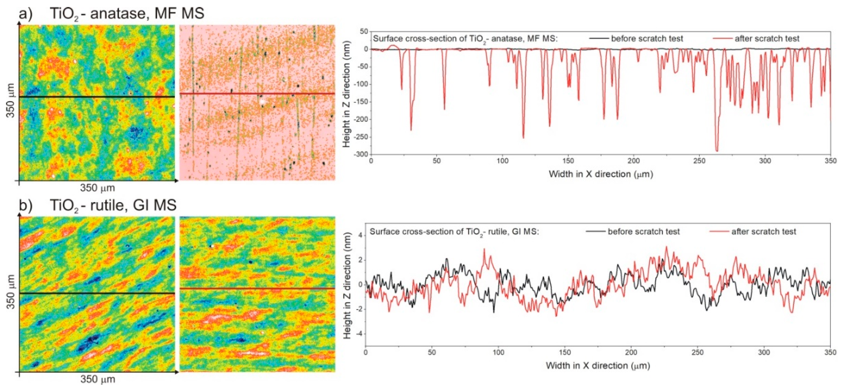
3.2. Surface Properties
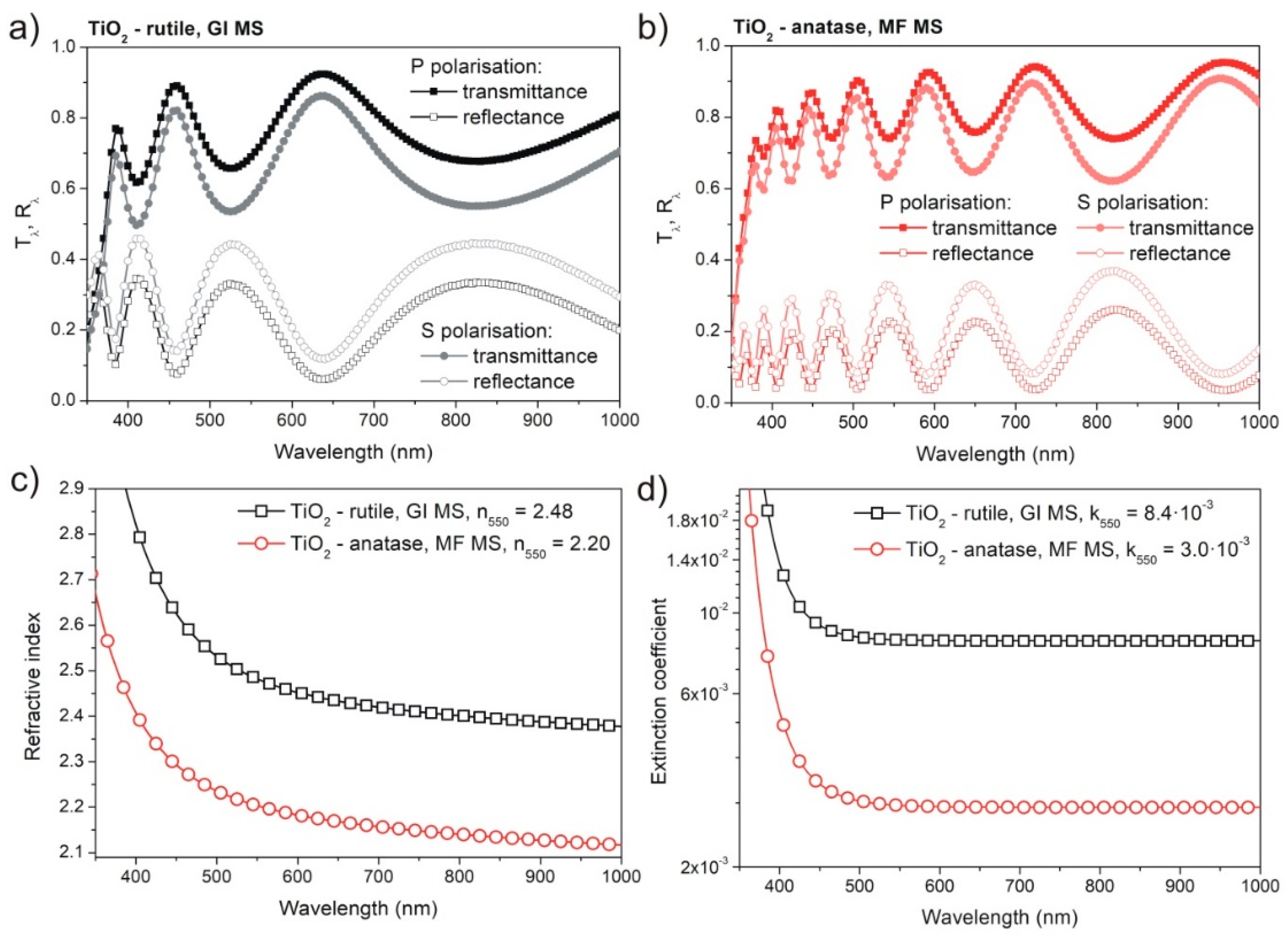
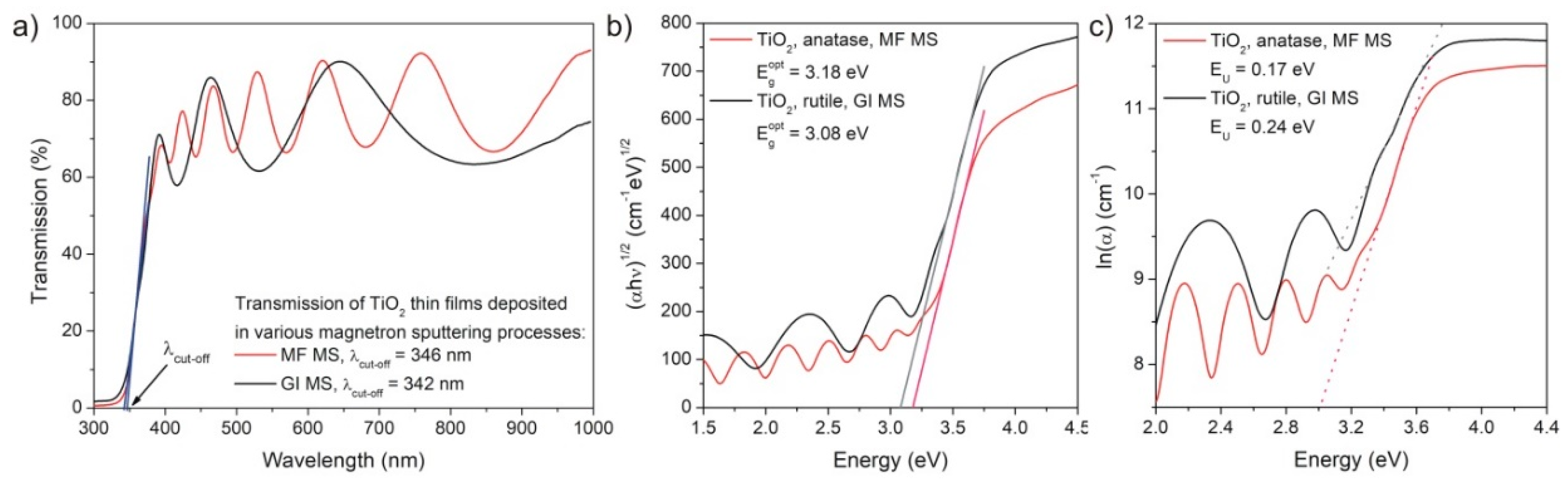
3.3. Optical Properties
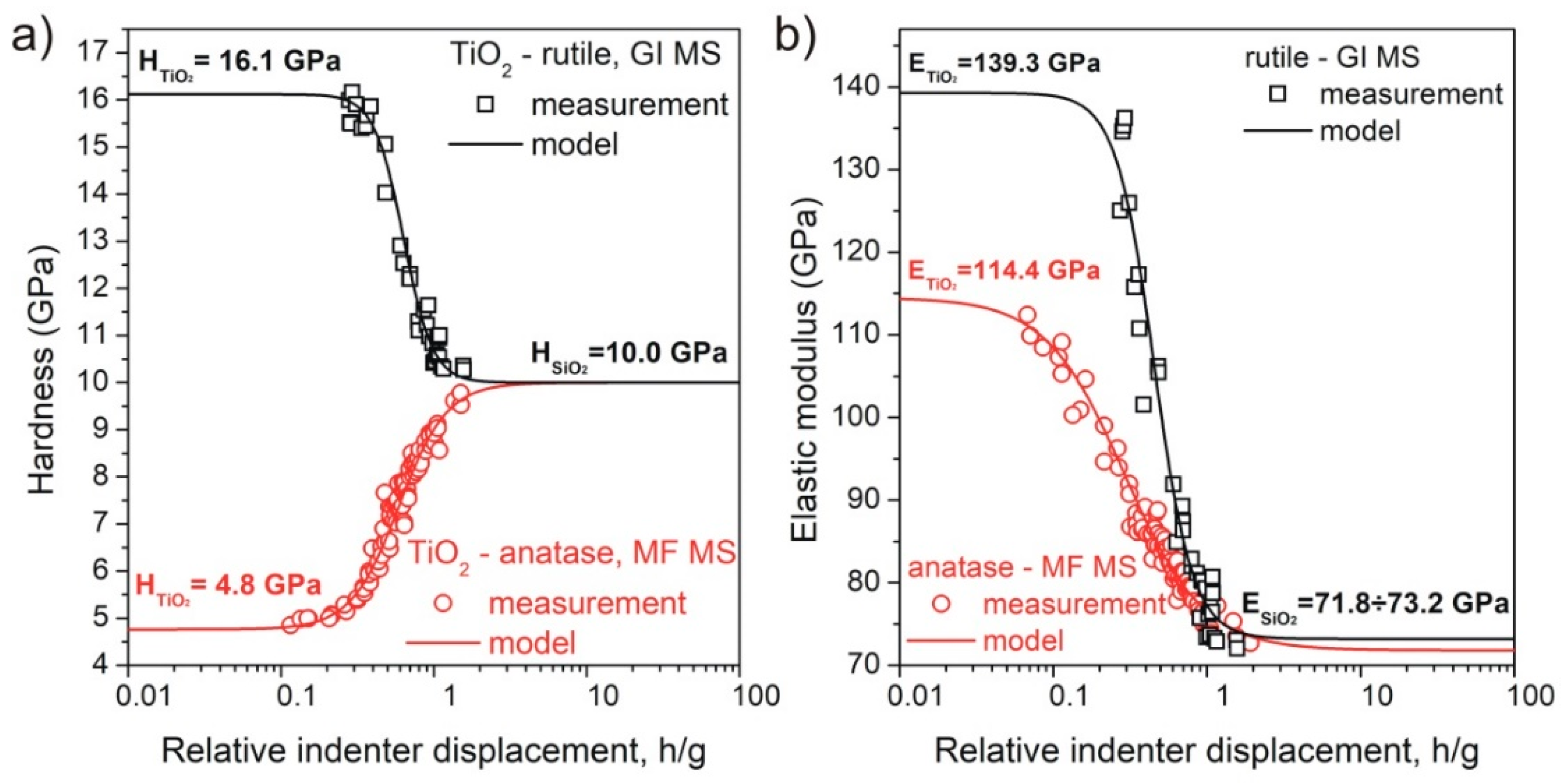
3.4. Mechanical Properties
4. Discussion
5. Conclusions
Author Contributions
Funding
Conflicts of Interest
References
- Nezar, S.; Saoul, N.; Sali, S.; Faiz, M.; Mekki, M.; Laoufi, N.A.; Tabet, N. Properties of TiO2 thin films deposited by rf reactive magnetron sputtering on biased substrates. Appl. Surf. Sci. 2017, 395, 172–179. [Google Scholar] [CrossRef]
- Vyas, S.; Tiwary, R.; Shubham, K.; Chakrabarti, P. Study the target effect on the structural, surface and optical properties of TiO2 thin film fabricated by RF sputtering method. Superlattices Microstruct. 2015, 80, 215–221. [Google Scholar] [CrossRef]
- Miller, M.J.; Wang, J. Coupled effects of deposition and annealing temperatures on optical, electrical and mechanical properties of titanium oxide thin films. Vacuum 2015, 120, 155–161. [Google Scholar] [CrossRef]
- Choi, K.H.; Duraisamy, N.; Muhammad, N.M.; Kim, I.; Choi, H.; Jo, J. Structural and optical properties of electrohydrodynamically atomized TiO2 nanostructured thin films. Appl. Phys. A 2012, 107, 715–722. [Google Scholar] [CrossRef]
- Wang, H.; Li, Y.; Ba, X.; Huang, L.; Yu, Y. TiO2 thin films with rutile phase prepared by DC magnetron co-sputtering at room temperature: Effect of Cu incorporation. Appl. Surf. Sci. 2015, 345, 49–56. [Google Scholar] [CrossRef]
- Lin, J.; Wang, B.; Sproul, W.D.; Ou, Y.; Dahan, I. Anatase and rutile TiO2 films deposited by arc-free deep oscillation magnetron sputtering. J. Phys. D Appl. Phys. 2013, 46, 084008. [Google Scholar] [CrossRef]
- Anders, A. Fundamentals of pulsed plasmas for materials processing. Surf. Coat. Technol. 2004, 183, 301–311. [Google Scholar] [CrossRef] [Green Version]
- Wiatrowski, A.; Posadowski, W.M.; Jóźwiak, G.; Serafińczuk, J.; Szeloch, R.; Gotszalk, T. Standard and self-sustained magnetron sputtering deposited Cu films investigated by means of AFM and XRD. Microelectron. Reliab. 2011, 51, 1203–1206. [Google Scholar] [CrossRef]
- Anders, A. Deposition rates of high power impulse magnetron sputtering: Physics and economics. J. Vac. Sci. Technol. A 2010, 28, 783–790. [Google Scholar] [CrossRef]
- Anders, A. Discharge physics of high power impulse magnetron sputtering. Surf. Coat. Technol. 2011, 205, S1–S9. [Google Scholar] [CrossRef] [Green Version]
- Wiatrowski, A.; Kijaszek, W.; Posadowski, W.M.; Oleszkiewicz, W.; Jadczak, J.; Kunicki, P. Deposition of diamond-like carbon films by the high power impulse magnetron sputtering method. Diamond Relat. Mater. 2017, 72, 71–76. [Google Scholar] [CrossRef]
- Vlček, J.; Rezek, J.; Houška, J.; Kozák, T.; Kohout, J. Benefits of the controlled reactive high-power impulse magnetron sputtering of stoichiometric ZrO2 films. Vacuum 2015, 114, 131–141. [Google Scholar] [CrossRef]
- Vlček, J.; Belosludtsev, A.; Rezek, J.; Houška, J.; Čapek, J.; Čerstvý, R.; Haviar, S. High-rate reactive high-power impulse magnetron sputtering of hard and optically transparent HfO2 films. Surf. Coat. Technol. 2016, 290, 58–64. [Google Scholar] [CrossRef]
- Wiatrowski, A.; Patela, S.; Kunicki, P.; Posadowski, W. Effective pulsed magnetron sputtering of aluminium oxide–Properties of films deposited utilizing automated process stabilizer. Vacuum 2016, 134, 54–62. [Google Scholar] [CrossRef]
- Posadowski, W.M.; Wiatrowski, A.; Dora, J.; Radzimski, Z.J. Magnetron sputtering process control by medium-frequency power supply parameter. Thin Solid Films 2008, 516, 4478–4482. [Google Scholar] [CrossRef]
- Skowronski, L.; Zdunek, K.; Nowakowska-Langier, K.; Chodun, R.; Trzcinski, M.; Kobierski, M.; Kustra, M.K.; Wachowiak, A.A.; Wachowiak, W.; Hiller, T.; et al. Characterization of microstructural, mechanical and optical properties of TiO2 layers deposited by GIMS and PMS methods. Surf. Coat. Technol. 2015, 282, 16–23. [Google Scholar] [CrossRef]
- Zdunek, K.; Nowakowska-Langier, K.; Chodun, R.; Dora, J.; Okrasa, S.; Talik, E. Optimization of gas injection conditions during deposition of AlN layers by novel reactive GIMS method. Mater. Sci.-Pol. 2014, 32, 171–175. [Google Scholar] [CrossRef] [Green Version]
- Zdunek, K.; Nowakowska-Langier, K.; Dora, J.; Chodun, R. Gas injection as a tool for plasma process control during coating deposition. Surf. Coat. Technol. 2013, 228, S367–S373. [Google Scholar] [CrossRef]
- Zdunek, K.; Skowronski, L.; Chodun, R.; Nowakowska-Langier, K.; Grabowski, A.; Wachowiak, W.; Okrasa, S.; Wachowiak, A.; Strauss, O.; Wronkowski, A.; et al. Novel GIMS technique for deposition of colored Ti/TiO2 coatings on industrial scale. Mater. Sci.-Pol. 2016, 34, 137–141. [Google Scholar] [CrossRef]
- Bukauskas, V.; Kaciulis, S.; Mezzi, A.; Mironas, A.; Niaura, G.; Rudzikas, M.; Šimkienė, I.; Šetkus, A. Effect of substrate temperature on the arrangement of ultra-thin TiO2 films grown by a dc-magnetron sputtering deposition. Thin Solid Films 2015, 585, 5–12. [Google Scholar] [CrossRef]
- Roy, S.S.; Bhuiyan, A.H. Surface morphology, compositional, optical and electrical properties of TiO2 thin films. Sens. Transducers 2015, 192, 66–73. [Google Scholar]
- Jiang, S.S.; Hea, G.; Gao, J.; Xiao, D.Q.; Jin, P.; Li, W.D.; Lv, J.G.; Liu, M.; Liu, Y.M.; Sun, Z.Q. Microstructure, optical and electrical properties of sputtered HfTiO high-k gate dielectric thin films. Ceram. Int. 2016, 42, 11640–11649. [Google Scholar] [CrossRef]
- Jin, P.; He, G.; Liu, M.; Xiao, D.Q.; Gao, J.; Chen, X.F.; Ma, R.; Zhang, J.W.; Zhang, M.; Sun, Z.Q.; et al. Deposition-power-modulated optical and electrical properties of sputtering-derived HfTiOx gate dielectrics. J. Alloy. Compd. 2015, 649, 128–134. [Google Scholar] [CrossRef]
- Oliver, W.C.; Pharr, G.M. An improved technique for determining hardness and elastic modulus using load and displacement sensing indentation experiments. J. Mater. Res. 1992, 7, 1564–1583. [Google Scholar] [CrossRef]
- ASTM F735-17 Standard Test Method for Abrasion Resistance of Transparent Plastics and Coatings Using the Oscillating Sand Method; ASTM International: West Conshohocken, PA, USA, 2017.
- JCPDS Card 21-1276 Powder Diffraction File; Joint Committee on Powder Diffraction Standards: Swarthmore, PA, USA, 1967.
- JCPDS Card 21-1272 Powder Diffraction File; Joint Committee on Powder Diffraction Standards: Swarthmore, PA, USA, 1967.
- Domaradzki, J.; Kaczmarek, D.; Prociow, E.L.; Wojcieszak, D.; Sieradzka, K.; Mazur, M.; Lapinski, M. Study of structural and optical properties of TiO2:Tb thin films prepared by high energy reactive magnetron sputtering method. Optica Applicata 2009, 39, 815–823. [Google Scholar]
- Wojcieszak, D.; Mazur, M.; Kaczmarek, D.; Morgiel, J.; Zatryb, G.; Domaradzki, J.; Misiewicz, J. Influence of Nd dopant amount on microstructure and photoluminescence of TiO2:Nd thin films. Opt. Mater. 2015, 48, 172–178. [Google Scholar] [CrossRef]
- Mazur, M.; Wojcieszak, D.; Domaradzki, J.; Kaczmarek, D.; Poniedziałek, A.; Domanowski, P. Investigation of microstructure, micro-mechanical and optical properties of HfTiO4 thin films prepared by magnetron co-sputtering. Mater. Res. Bull. 2015, 72, 116–122. [Google Scholar] [CrossRef]
- Danish, R.; Ahmed, F.; Arshi, N.; Anwar, M.S.; Koo, B.H. Facile synthesis of single crystalline rutile TiO2 nano-rods by solution method. Trans. Nonferrous Met. Soc. China 2014, 24, s152–s156. [Google Scholar] [CrossRef]
- Alhomoudi, I.A.; Newaz, G. Residual stresses and Raman shift relation in anatase TiO2 thin film. Thin Solid Films 2009, 517, 4372–4378. [Google Scholar] [CrossRef]
- Gupta, S.K.; Singh, J.; Anbalagan, K.; Kothari, P.; Bhatia, R.R.; Mishra, P.K.; Manjuladevi, V.; Gupta, R.K.; Akhtar, J. Synthesis, phase to phase deposition and characterization of rutile nanocrystalline titanium dioxide (TiO2) thin films. Appl. Surf. Sci. 2013, 264, 737–742. [Google Scholar] [CrossRef]
- Kadam, R.M.; Rajeswari, B.; Sengupta, A.; Achary, S.N.; Kshirsagar, R.J.; Natarajan, V. Structural characterization of titania by X-ray diffraction, photoacoustic, Raman spectroscopy and electron paramagnetic resonance spectroscopy. Spectrochim. Acta Part A 2015, 137, 363–370. [Google Scholar] [CrossRef] [PubMed]
- Kwok, D.Y.; Neumann, A.W. Contact angle measurement and contact angle interpretation. Adv. Colloid Interface Sci. 1999, 81, 167–249. [Google Scholar] [CrossRef]
- Sharfrin, E.; Zisman, W.A. Constitutive relations in the wetting of low energy surfaces and the theory of the retraction method of preparing monolayer. J. Phys. Chem. 1960, 64, 519–524. [Google Scholar] [CrossRef]
- Leyland, A.; Matthews, A. On the significance of the H/E ratio in wear control: a nanocomposite coating approach to optimized tribological behaviour. Wear 2000, 246, 1–11. [Google Scholar] [CrossRef]
- Chang, L.C.; Chang, C.Y.; Chen, Y.I. Mechanical properties and oxidation resistance of reactively sputtered Ta1−xZrxNy thin films. Surf. Coat. Technol. 2015, 280, 27–36. [Google Scholar] [CrossRef]
- Dave, V.; Dubey, P.; Gupta, H.O.; Chandra, R. Influence of sputtering pressure on the structural, optical and hydrophobic properties of sputtered deposited HfO2 coatings. Thin Solid Films 2013, 549, 2–7. [Google Scholar] [CrossRef]
- Bauer, G. Absolutwerte der optischen Absorptionskonstanten von Alkalihalogenidkristallen im Gebiet ihrer ultravioletten Eigenfrequenzen. Ann. Phys. 1934, 411, 434–464. [Google Scholar] [CrossRef]
- Patschaider, J. Nano-composite hard coatings for wear protection. MRS Bull. 2003, 28, 180–183. [Google Scholar] [CrossRef]
- Vepřek, S.; Reiprich, S. A concept for the design of novel superhard coatings. Thin Solid Films 1995, 268, 64–71. [Google Scholar] [CrossRef]


| Thin Film | Phase | Crystal Plane | D (nm) | d (nm) |
|---|---|---|---|---|
| PDF No. 21-1272 TiO2 | anatase | - | - | 0.3520 |
| TiO2 (MF MS) | anatase | (101) | 36.1 | 0.3511 |
| PDF No. 21-1276 TiO2 | rutile | - | - | 0.3247 |
| TiO2 (GI MS) | rutile | (110) | 11.0 | 0.3266 |
© 2018 by the authors. Licensee MDPI, Basel, Switzerland. This article is an open access article distributed under the terms and conditions of the Creative Commons Attribution (CC BY) license (http://creativecommons.org/licenses/by/4.0/).
Share and Cite
Wiatrowski, A.; Mazur, M.; Obstarczyk, A.; Wojcieszak, D.; Kaczmarek, D.; Morgiel, J.; Gibson, D. Comparison of the Physicochemical Properties of TiO2 Thin Films Obtained by Magnetron Sputtering with Continuous and Pulsed Gas Flow. Coatings 2018, 8, 412. https://doi.org/10.3390/coatings8110412
Wiatrowski A, Mazur M, Obstarczyk A, Wojcieszak D, Kaczmarek D, Morgiel J, Gibson D. Comparison of the Physicochemical Properties of TiO2 Thin Films Obtained by Magnetron Sputtering with Continuous and Pulsed Gas Flow. Coatings. 2018; 8(11):412. https://doi.org/10.3390/coatings8110412
Chicago/Turabian StyleWiatrowski, Artur, Michał Mazur, Agata Obstarczyk, Damian Wojcieszak, Danuta Kaczmarek, Jerzy Morgiel, and Des Gibson. 2018. "Comparison of the Physicochemical Properties of TiO2 Thin Films Obtained by Magnetron Sputtering with Continuous and Pulsed Gas Flow" Coatings 8, no. 11: 412. https://doi.org/10.3390/coatings8110412