
Effect of the Microstructure of ZnO Thin Films Prepared by PLD on Their Performance as Toxic Gas Sensors


1
Unité de Dynamique et Structure des Matériaux Moléculaires (UDSMM), Université du Littoral Côte d’Opale (ULCO), BP717, 62228 Calais, France
2
Université de Rennes, CNRS, ISCR-UMR 6226, F-35000 Rennes, France
*
Author to whom correspondence should be addressed.
Chemosensors 2022, 10(7), 285; https://doi.org/10.3390/chemosensors10070285
Submission received: 25 May 2022
/
Revised: 8 July 2022
/
Accepted: 12 July 2022
/
Published: 16 July 2022
(This article belongs to the Special Issue The State-of-the-Art Gas Sensor)
Abstract
:In 2008, the modified European Restriction of Hazardous Substances (RoHS) directive prohibited the use of hazardous substances such as lead, cadmium, and mercury. As such, an urgent need for lead-free components emerged in Europe. In this frame, we have decided to study the microstructure influence of zinc oxide thin films on the detection of hydrogen sulfide (H2S). Zinc oxide thin films were deposited by PLD on silicon substrates under different conditions to modify the microstructure. In order to compare our demonstrators to current commercial semiconductor gas sensors, measurements under H2S were also performed with sensors from Figaro and Winsen corporations. Gas sensors were therefore implemented by using commercial cases in view to test them with Simtronics gas detector DG477. The good sensitivity values measured at T = 400 °C under 100 ppm H2S, and response times as low as 30 s, definitely confirm that ZnO thin films could be developed for commercial sensors.
1. Introduction
In 2008, the modified European Restriction of Hazardous Substances (RoHS) directive prohibited the use of hazardous substances such as lead, cadmium, and mercury. As such, an urgent need for lead-free components emerged in Europe. The global industry of electronics is therefore trying to produce components and devices which comply with RoHS standards. For the detection of dangerous toxic and flammable gases in industrial sites, oxides have been studied and implemented for the development of gas sensors, and especially semiconductor gas sensors [1,2,3,4,5]. For this sensor technology, the material of the oxidation–reduction mechanism is generally a semiconductor metallic oxide with n or p-type behavior. Here, a lot of studies have been completed, such as on the well-known SnO2 or ZnO, in which conduction is due to oxygen vacancies because the oxide is not exactly stoichiometric [6,7,8]. The redox reactions, or simply adsorption to the surface, will change the resistivity of the material, by varying the number of charge carriers. In this application, the sensible material is heated for reaching the maximum sensitivity, and the variation of the material resistance is measured to determine the sensing parameters. The heating element is only used to control the operating temperature. However, the heating power must be managed because it is the most important part of the total electrical power consumption of the sensor. The sensing measurement range of these devices depends on the implemented signal processing: either the range 0–100% LLE (low limit of explosivity) or the range 0–100% v/v, the range ppm. Among their properties, semiconductor gas sensors are well-known for their non-selectivity in non-optimized conditions [9,10]. So, high selectivity is one of the main challenges of semiconductor gas sensors. Enhancing the selective properties is mainly completed by two approaches. The first one is performed by investigating the optimal operating temperature, doping elements, and their concentrations [7,8,9]. The second one is usually performed by modulation of the sensor operating temperature [11,12,13,14,15] or by using sensor arrays as electronic noses [16,17]. Sensitivity to various compounds will also depend on the gas calibration, like for catalytic sensors. Additionally, they require the presence of oxygen to function [3,4,6,10]. Indeed, the presence of oxygen in the background determines a higher baseline resistance due to the formation of ionosorbed oxygen. This effect generally increases the response and recovery times. For the detection of flammable gases, semiconductor sensors are not very used in industrial applications, because they age due to heating and thus derive very rapidly, i.e., within weeks for some. In addition, these sensors are influenced by ambient conditions, particularly by moisture [4,6,10]. The moisture influence is also confirmed by corporations for commercial gas sensors [18,19,20]. The water vapor adsorbed onto the surface of the semiconductor is an interfering problem. The dynamic response of these sensors is very variable, and the response time can range from a few tens of seconds to several minutes [5,6,7,8,9]. Their lifetime is of the order of several weeks to several years, depending on the context of use. Therefore, the use of SC gas sensors is not recommended for the detection of flammable gas. In contrast, semiconductor oxides can be used for the detection of toxic gases and vapors. Moreover, our industrial partner, SIMTRONICS SAS, is particularly interested in cost-effective semiconductor gas sensors dedicated to the detection of hydrogen sulfide (H2S), as one of its main markets is related to oil production sites. H2S is a colorless, toxic gas with a strong smell of rotten eggs; it is present in a natural way (crude oil, natural gas, volcanic gas …) but is also produced by human activities (oil refinery, petrochemical industry, food processing industry …). The human olfactory sensitivity to H2S is low (0.014 ppm) but our ability to detect this gas decreases when its concentration increases and disappears around 100 ppm, and H2S can cause death beyond 800 ppm. Today, occupational exposure limit values in workplace air are less than 10 ppm (1 ppm for the more restrictive value). In this frame, we have decided to study the influence of the microstructure of zinc oxide (ZnO) thin films on the detection of hydrogen sulfide (H2S). In this way, zinc oxide thin films were deposited by PLD on silicon substrates under different conditions to modify their microstructure. In the present work, we report first results obtained with lead-free ZnO oxide as semiconductor gas sensors. ZnO thin films were deposited by pulsed laser deposition on Si (100) and SiO2/Si (100) substrates. A detailed study of the influence of the substrate temperature and the oxygen pressure during the deposition on the phase formation, and the microstructure, and the electrical properties was first performed on ZnO/Si (100). The objective was to obtain regular films with various structural and microstructural characteristics and to correlate these with the results of the sensor measurements.
2. Experimental Section
The ZnO thin films were grown on commercial single-crystalline Si (100) and SiO2/Si (100) substrates. They were deposited from a homemade sintered target by pulsed laser deposition using a KrF excimer laser (λ = 248 nm) with a focused energy density of about 2 J/cm2 and a pulse duration of 20 ns. The three variable deposition parameters were the laser frequency: between 2 to 5 Hz; the temperature: from room temperature (RT) to 700 °C, and the atmosphere: from vacuum to oxygen pressure between 6 × 10⁻² to 1 mbar. The structural analyses were performed by X-ray diffraction using a D8 Advanced Brüker AXS (θ−2θ configuration) equipped with a monochromatized Cu Kα1 radiation source. Microstructural characterizations, mainly surface morphology, and thickness, were determined by field-emission scanning electron microscopy (FE-SEM), using a JEOL JSM 6310F system working at a low accelerating voltage (7–9 kV) in order to limit charge effects and to achieve a high resolution without causing surface metallization. The sheet resistance of samples was directly measured with the 4 probes method. For the electrical characterizations and tests under gas, interdigitated electrodes were prepared by optical lithography and deposition of gold by vacuum evaporation. The distance between fingers of interdigitated electrodes was kept to 100 µm for all sensors. The resistance of films was measured by an HP4284A impedance analyzer using the interdigitated electrodes deposited onto the film surface. For all measurements under gas exposure, the prepared samples were glued to a heater. Then, both films and heaters were embedded in commercial cases. The 100 ppm hydrogen sulfide was bought from a commercial provider. For lower concentrations, it was diluted with different ratios of dry air (commercial synthetic air). The hydrogen sulfide, with different concentrations, or air, was directly injected into the nose of the Simtronics gas detector DG 477. Weak flows were only used for avoiding temperature variations of the gas sensor.
3. Results
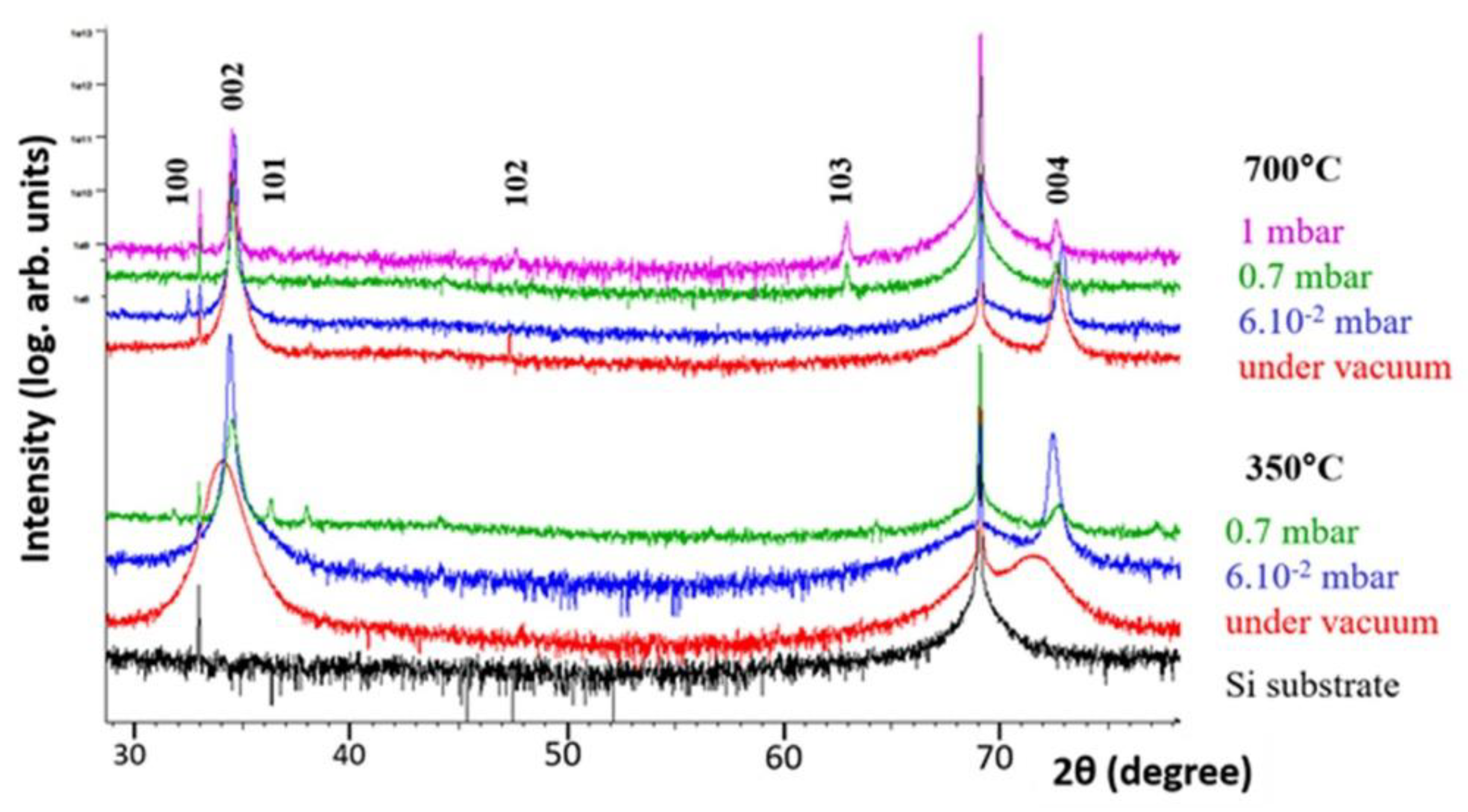
Figure 1 shows the θ–2θ X-ray diffraction (XRD) patterns of ZnO thin films deposited by PLD on Si (100) substrates, at 350 °C and 700 °C, under vacuum or under various oxygen pressures (6 × 10⁻², 0.7 and 1 mbar), with a fixed laser frequency (5 Hz) and a deposit duration varying from 10 to 30 min. Detailed conditions are summarized in Table 1.
Pure ZnO phase is obtained whatever the deposition conditions are, and all peaks are indexed in a Würtzite-type structure (ICDD PDF Card n°00-080-0075). Two intense peaks, indexed as the (002) and (004) reflections of the hexagonal structure, show that the films present a high c-axis oriented growth, as usually observed with Si or glass substrates and whatever the deposition method [21,22,23,24,25]. The presence of native oxide on the surface of the substrate, and more precisely oxygen atoms, leads to a preferential attraction of Zn atoms; in the Würtzite structure, the higher density of Zn atoms is along the (00ℓ) planes, which could favor this growth orientation [25]. However, the pressure increase leads to polycrystalline growth, regardless of the deposition temperature.
The lattice c constant of the ZnO thin films were calculated from the (002) diffraction peak position (°2θ); both values are listed in Table 1. According to the ICDD PDF card, the bulk value of the (002) peak position and the c parameter is, respectively, 2θ = 34.40° and c = 5.2098 (3) Å at 350 °C, the pressure increase induces a shift of this peak position towards wide angles whereas c parameter decreases. The C9 and C10 samples have higher c lattice constants than the bulk ones, which implies tensile stress; in contrast, other films are under compressive stress [26].
Additionally, when the pressure increases, mainly at 350 °C, the peaks become thinner. The broadening of the (002) peak can be used to determine the crystallite size (D) of the films, by using the Debye–Scherrer formula:
where λ = 0.15406 nm is the wavelength of the X-ray radiation, θ is the Bragg angle of the (002) reflection, β is the full width at half maximum (FWHM) of the diffraction peak and β0 is the width related to the instrumental broadening (both measured in radian) and K = 0.9 when using the FWHM. The results are presented in Table 1.
As expected, and already observed [25], the crystalline quality of the films deposited is enhanced at higher temperature; all films deposited at 700 °C have FWHM values lower than 0.13° with corresponding crystallite sizes larger than 70 nm. On the contrary, a FWHM value around 0.9° associated to a crystallite size of around 10 nm is observed for the film deposited under vacuum at 350 °C, in agreement with the broad peaks shown on Figure 1. At 700 °C, no significant influence of the oxygen pressure was observed, whereas the quality of the film is strongly enhanced with oxygen at 350 °C. Whatever the temperature, better results are obtained under an oxygen pressure of 0.06 mbar.
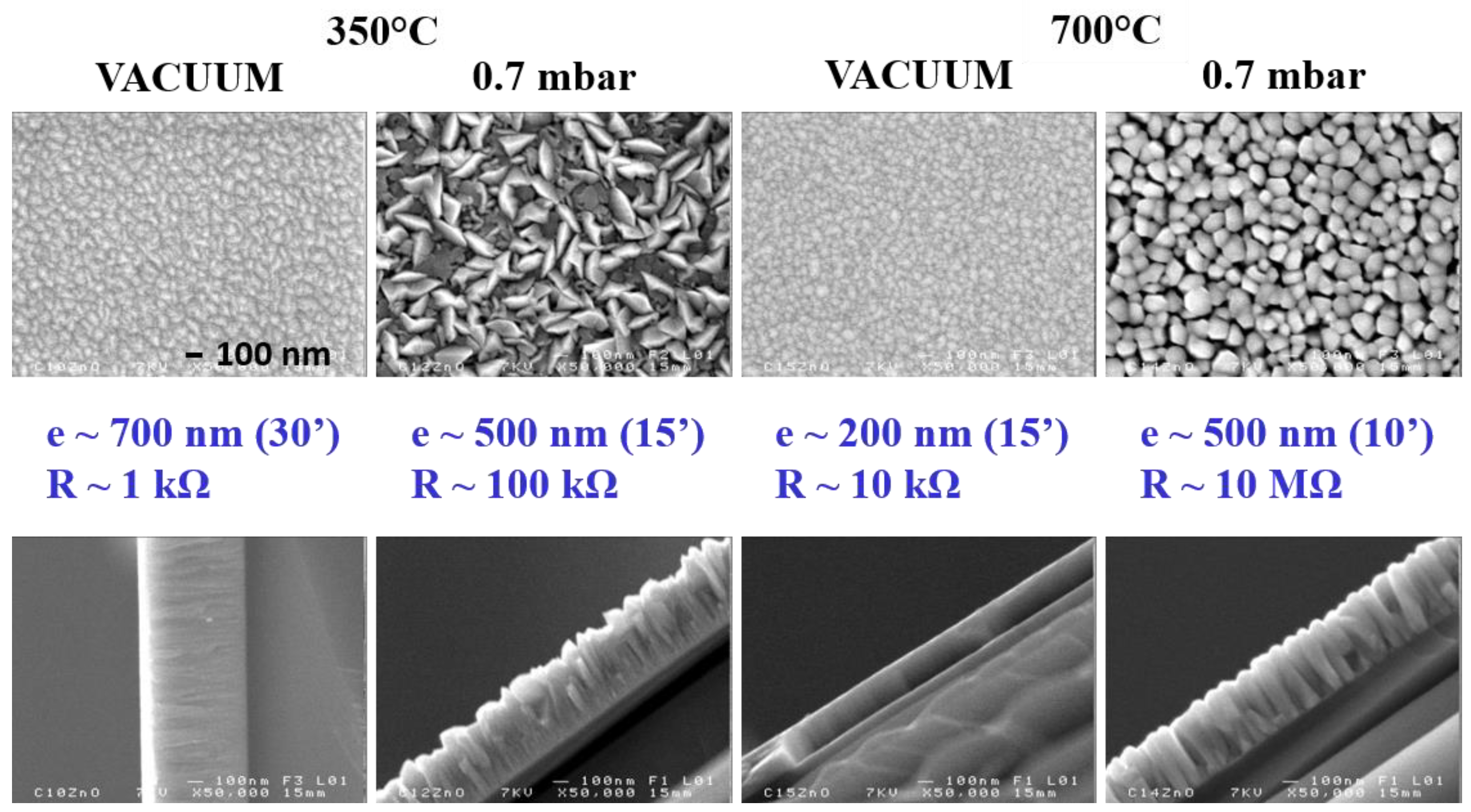
The morphology of the thin films is strongly dependent on the deposition conditions as illustrated in Figure 2. Dense and continuous films were obtained under vacuum and with 0.06 mbar oxygen pressure (not shown), while porous films formed by quite circular grains of 100 to 150 nm in diameter are observed at 700 °C with oxygen. At 350 °C under oxygen, the shape of the grains is quite different: large and more or less flat grains of various shapes appear. However, all films present a columnar growth. The films have a thickness ranging from 200 to 700 nm and a resistance varying from 1 kΩ to 10 MΩ also depending on the deposition conditions; thus, at a fixed temperature, a higher oxygen pressure leads to a thicker film with higher electrical resistance. Under exposition to oxygen and when the deposition temperature is increased, then the film thickness and its resistance increase. Similarly, and as expected, the increase in laser frequency or deposition time increases the thickness of the film, but on the other hand, induces a decrease in its resistance. The grain size increases with the oxygen pressure as clearly shown in Figure 2. So, the c-axis oriented growth and the microstructure of ZnO/Si (100) thin films can be perfectly tuned by the deposition conditions.
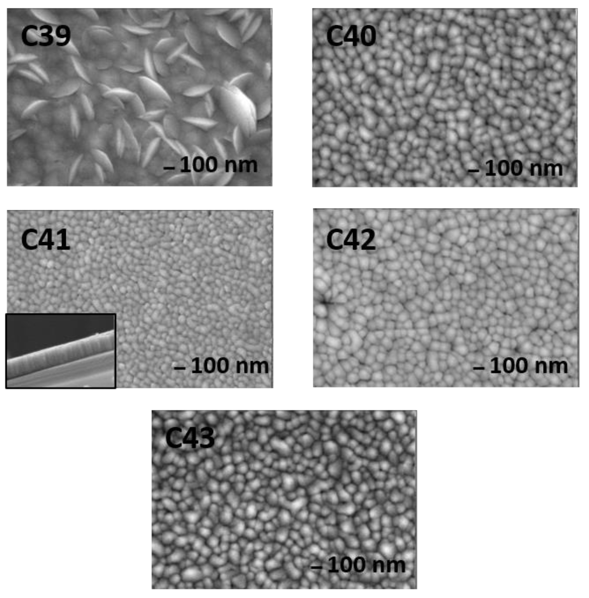
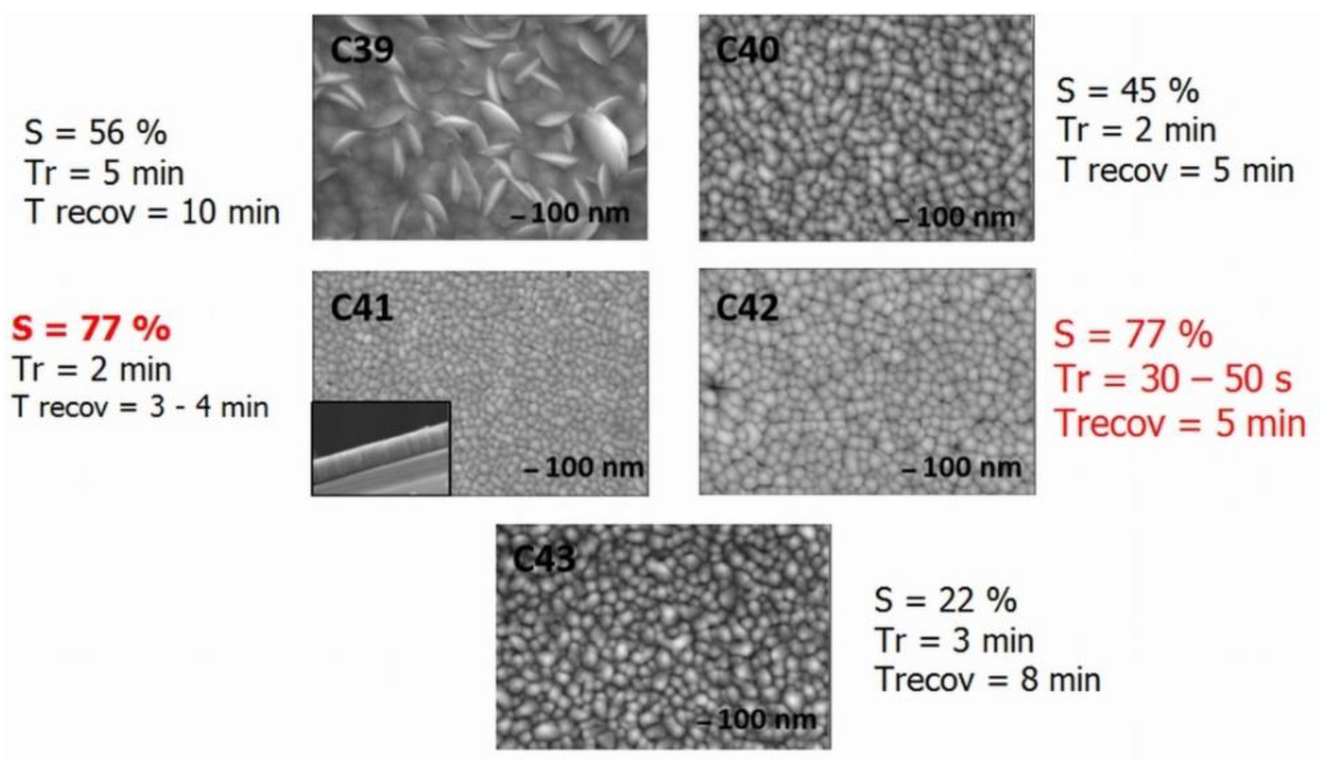
For our purpose, i.e., gas sensing, we need porous films with controlled grain size for increasing the adsorption/desorption of gas. For all characterizations under different conditions of gas exposure, thin films were deposited on SiO2/Si (100) substrates, where the SiO2 layer was 1 µm thick. Under the same deposition conditions, the ZnO thin films deposited on Si (100) and on SiO2/Si (100) substrates have the same orientation and microstructure, but the layer thickness and the grain size are smaller on SiO2/Si than on Si. Five thin films, labelled C39 to C43, were deposited by pulsed laser deposition on SiO2/Si substrates, from the same target, and using conditions optimized for gas detection. The deposition conditions of these selected films are summarized in Table 2. In order to evaluate the reproducibility of the gas detection results, two films were made each time under the same deposition conditions.
The XRD patterns (not shown) of all ZnO/SiO2/Si (100) thin films match a Würtzite-type ZnO pure phase, with a (00ℓ) preferential orientation; a small (101) diffraction peak, (i.e., the most intense peak of ZnO powder) is observed for C39 and C42.
All films have a homogeneous, rather dense surface. The same morphologies than those already observed for ZnO/Si films are found again; large flat disk-shaped grains (200 ≤ Ø ≤ 400 nm) in case of C39 or small quite circular grains (30 ≤ Ø ≤ 150 nm) for C40 to C43, with a columnar growth (Figure 3). The film thicknesses are, respectively, around 450 nm (C40 and C41), 500 nm (C43), 600 nm (C39) and 1000 nm (C42).
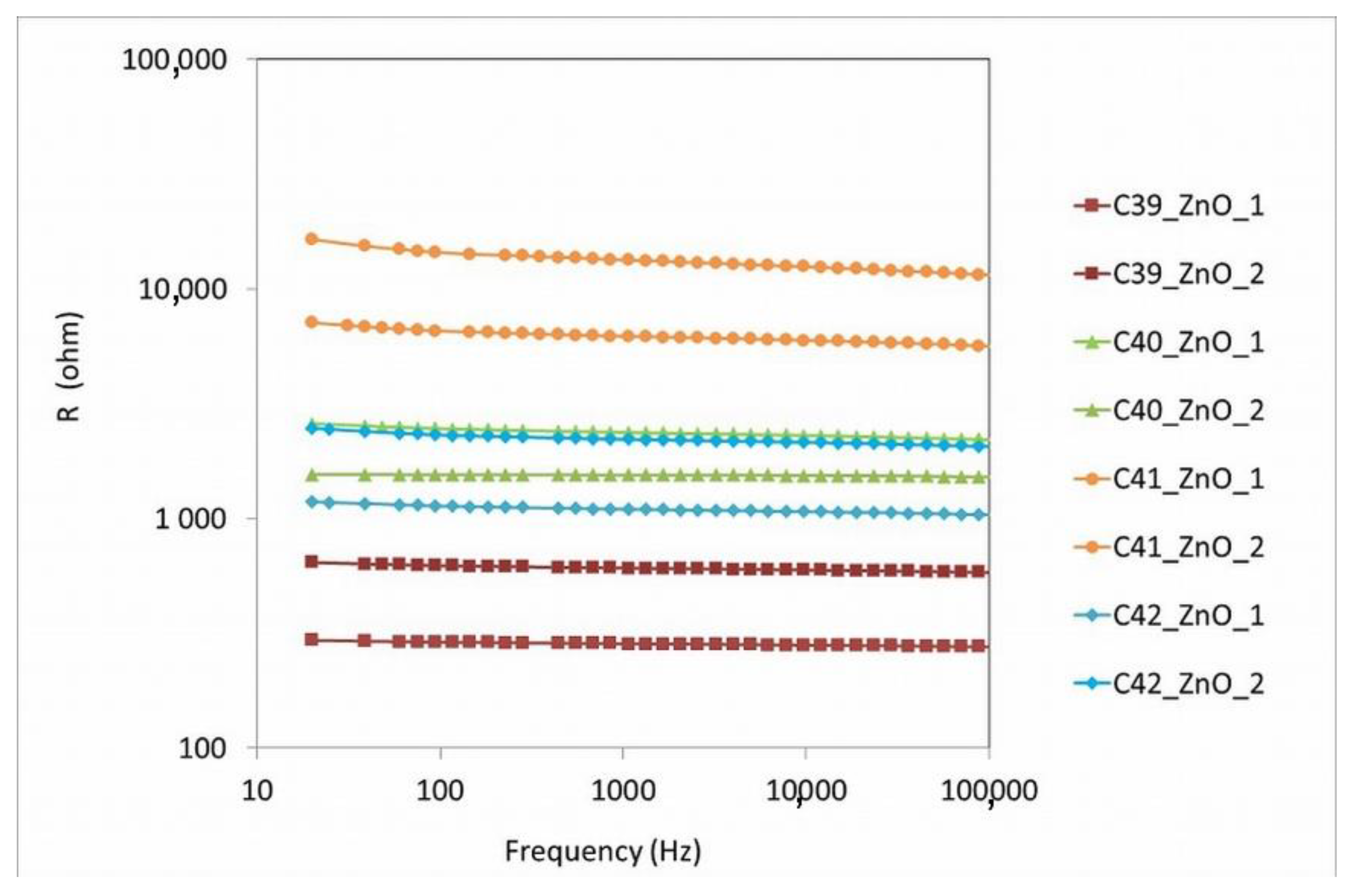
Before the integration in gas sensor packages, AC measurements were performed for measuring the evolution of film resistances. So, we only give here the real part of the measured impedance, as the sample (here in inter-digitated configuration) model is a parallel (R,C) model. The knowledge of the resistance value was important because the electronic conditioner was designed in function of this value. The results are given in Figure 4 in the 20 Hz to 1 MHz frequency range, for two samples of each kind of film. The lowest values were measured on the film C39 with values always lower than 1 kΩ. The highest ones were given by film C41 with values around 10 kΩ. The evolution of the resistance can be easily linked to the microstructure differences. The film C39 is completely different when compared to the four others, because it is not composed of circular grains, but mainly of disc-like grains arranged in different directions. The film C41 is very dense and composed of very fine grains, mainly circular, of diameters ranging from 30 to 90 nm. Between these two films, the others show a microstructure similar to film C41, but with bigger grains.
Measurements under the Exposure of H2S
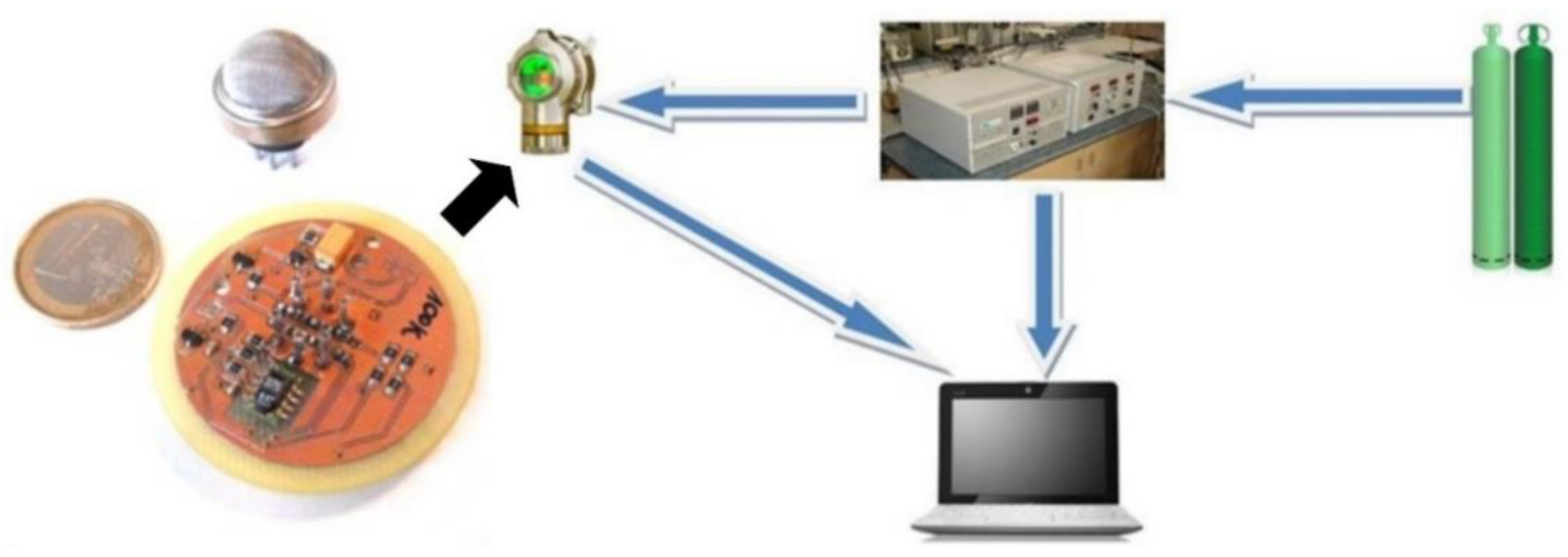
Finally, the ZnO thin films were embedded in commercial cases for all measurements under gas. An example of a semiconductor gas sensor is presented in Figure 5. Here, it is necessary to be reminded that a semiconductor (SC) gas sensor is composed of three different parts: (a) the heater used for tuning the operating temperature because SC gas sensors generally show a peak of sensitivity for temperatures ranging from 200 to 500 °C; (b) the oxide sensitive film deposited onto a substrate; (c) metallic interdigitated electrodes deposited onto the film surface for the electrical measurements.
In the following text, we will use the terms “response” and “sensitivity” synonymously, because they are both used by the community. For reducing gas, the sensor response S is given by:
where R is the measured resistance under the test gas, R0 is the resistance in the initial conditions (under air, measurement temperature). In the case of oxidizing gas, S = (R − R0)/R0.
S = (R0 − R)/R
The gas sensor is mounted on an electronic card for signal conditioning. Then, the e-card is placed into the nose of the Simtronics gas detector DG 477. The complete measurement setup is presented in Figure 6. This setup is controlled by software developed by our industrial partner.
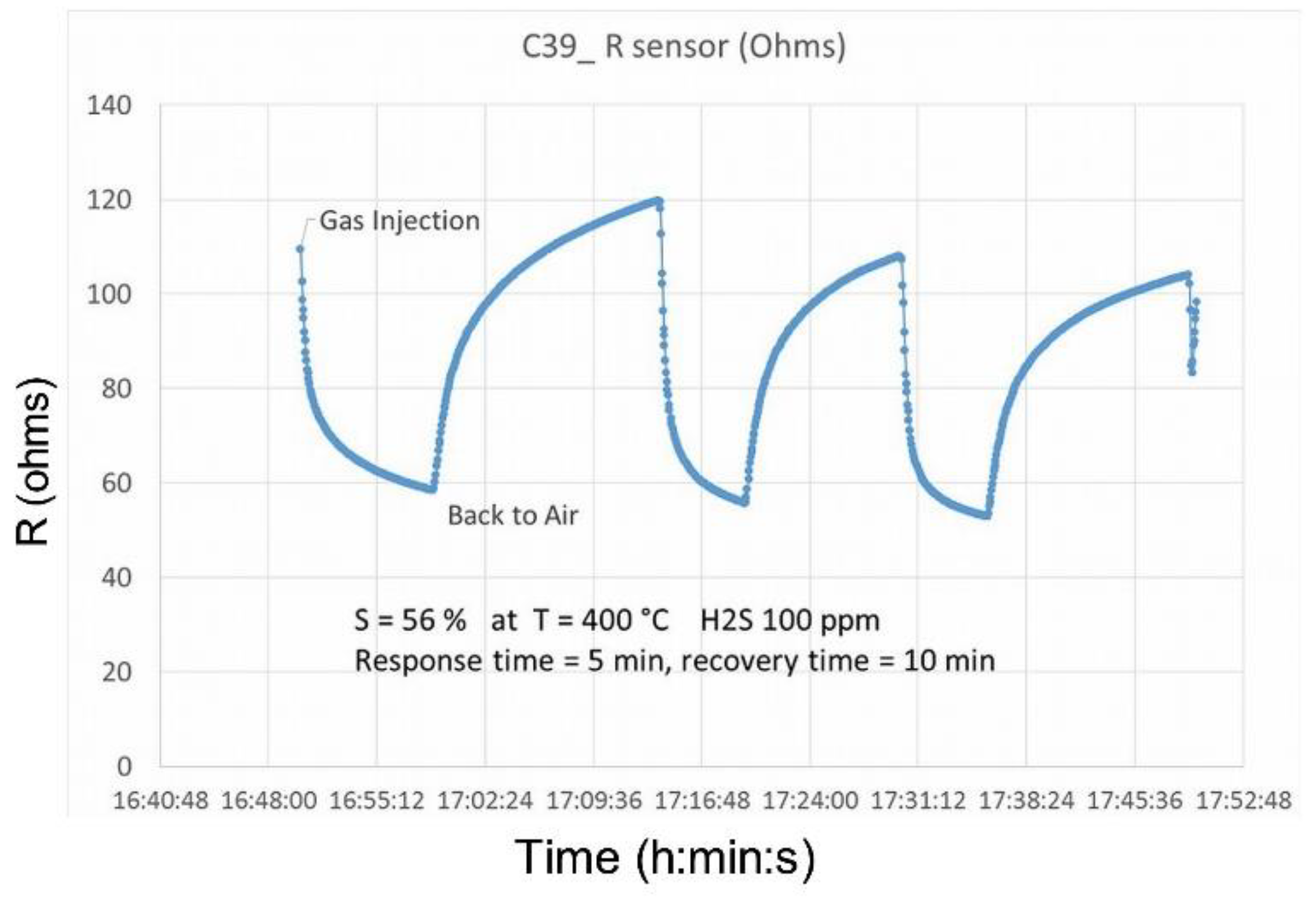
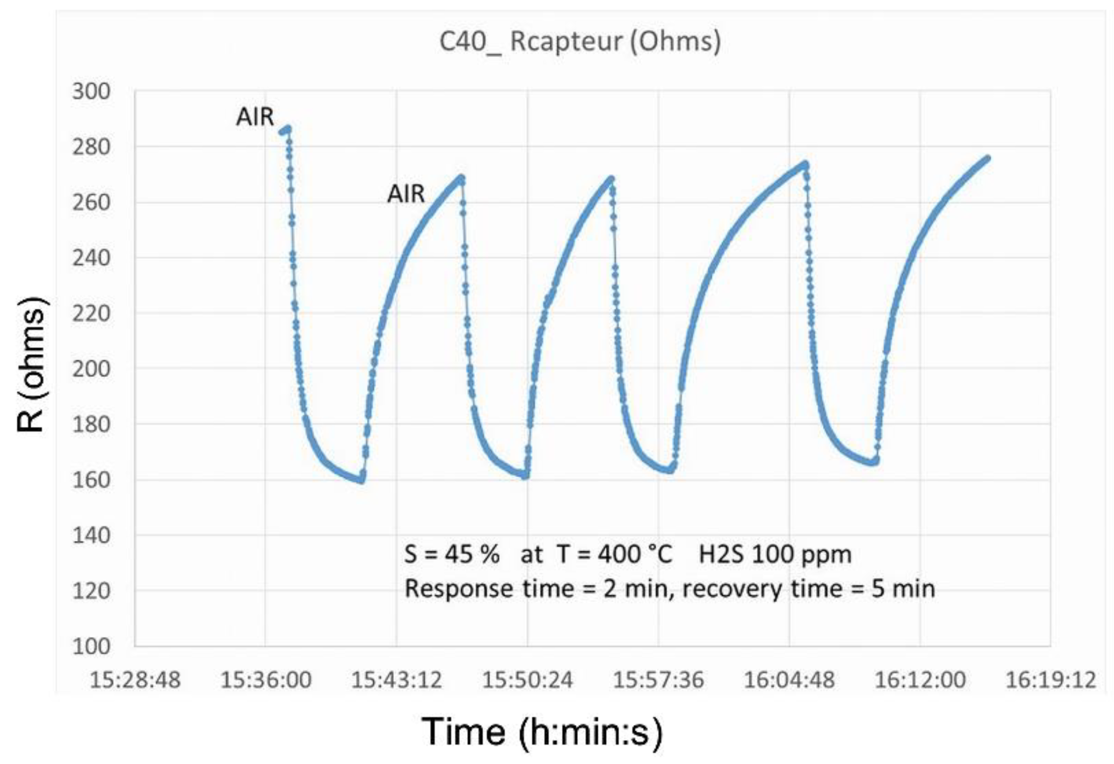
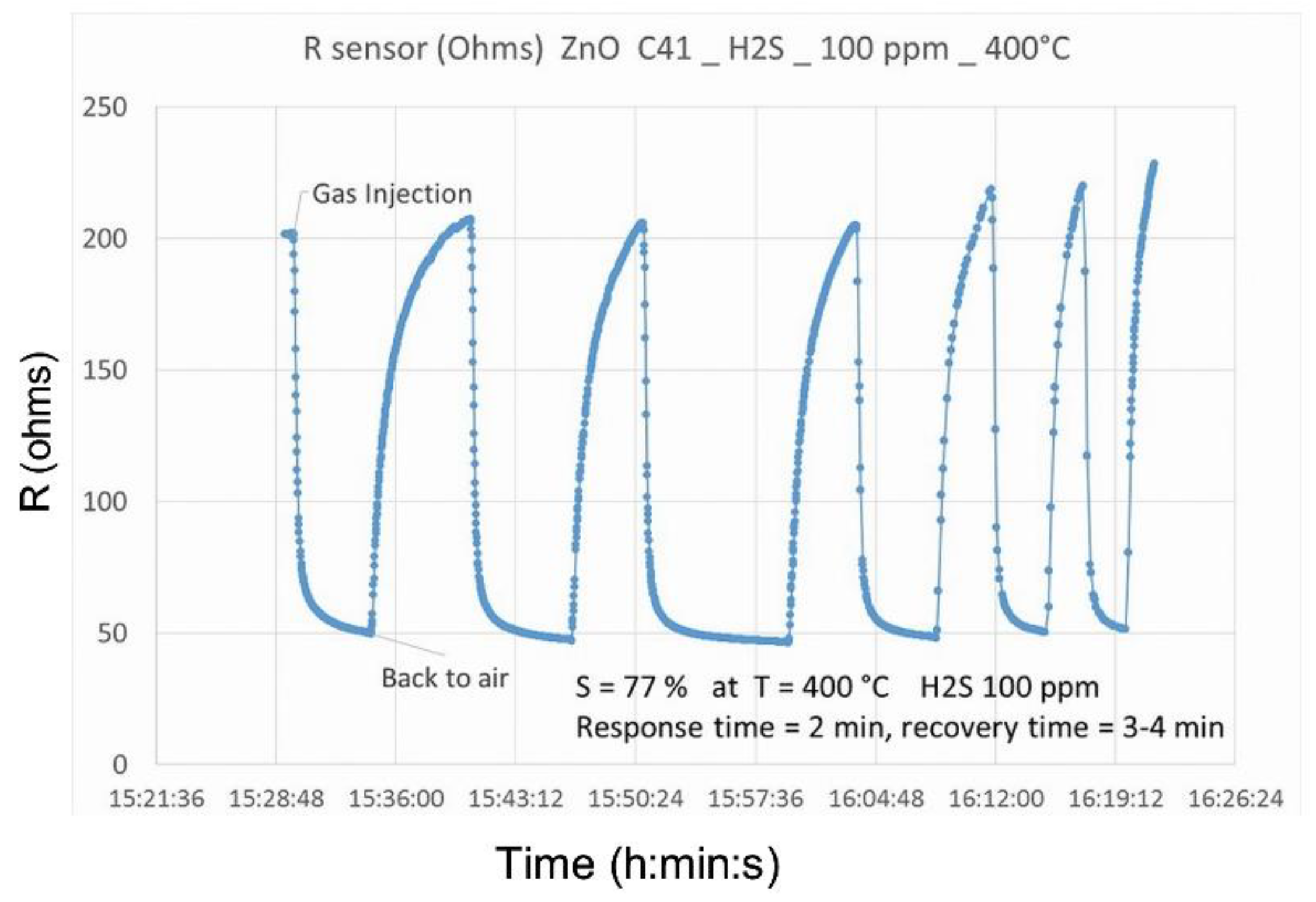
All gas sensors were tested under different concentrations of H2S and in a large temperature range for defining the optimal operating temperature with the maximum sensitivity. The ZnO sensors have given an optimal response at 400 °C. In view to compare our results to current commercial semiconductor gas sensors, measurements under H2S were also completed with sensors from Figaro and Winsen corporations [18,19,20]. All the results on the sensitivity under 100 ppm H2S concentration are plotted in Figure 7, Figure 8, Figure 9, Figure 10 and Figure 11. The sensitivity value calculated from Equation (2) is given on each figure. The average sensitivity values of the ZnO sensors are really of interest, as no optimization of the sensor volume was performed to increase the sensitivity at this time. About the dynamic response, all values of response and recovery times are also given in each figure. These dynamic time values were measured for a response of 90% of the complete response, i.e., when reaching saturation.
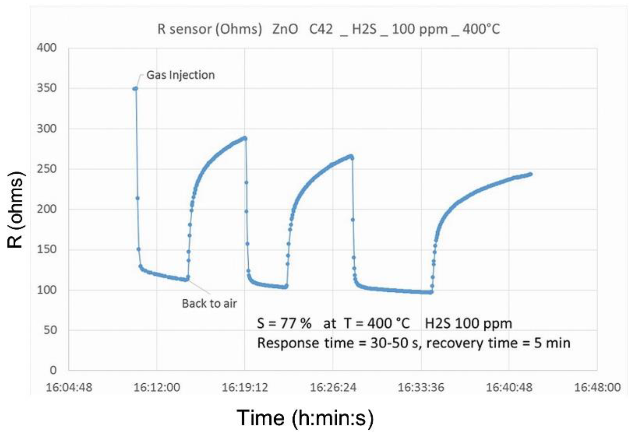
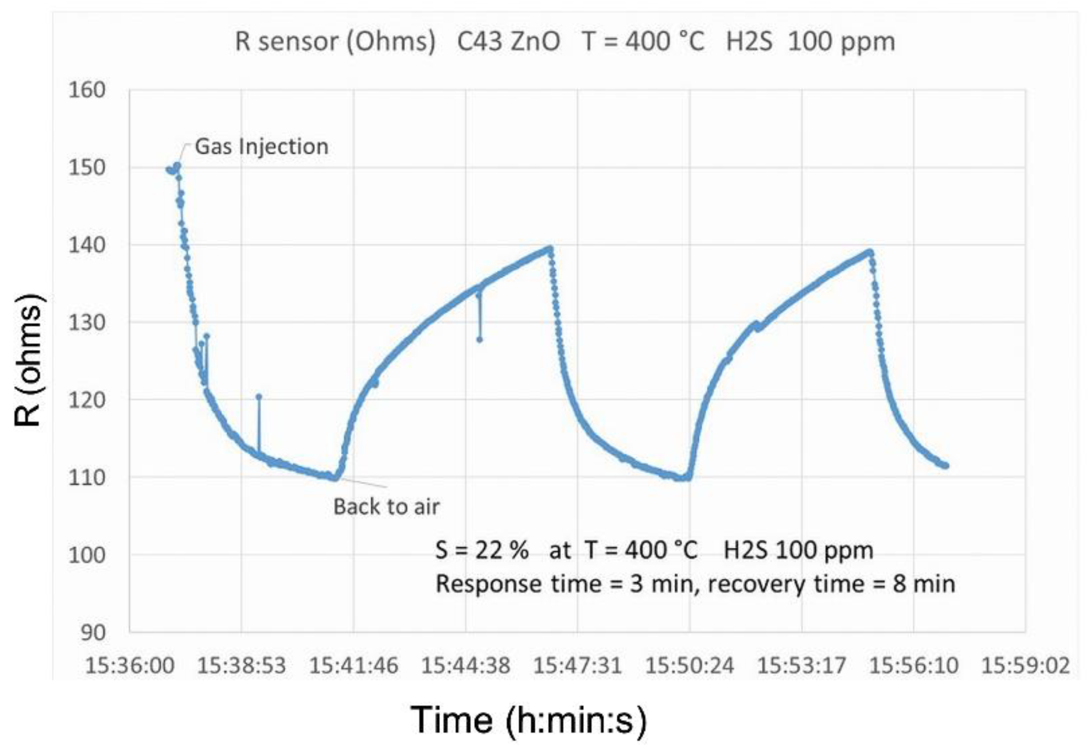
For all films, the response under H2S is significant with sensitivity ranging from 22 to 77%. The film C39 displays a sensitivity of 56% with the longest times of response and recovery. This film microstructure is made of disc-like grains, which are relatively big. In fact, the film C39 shows grains of length higher than 200 nm and is randomly oriented. This polycrystalline growth is confirmed by its XRD pattern. The films C40 to C43 display a homogeneous and well-compact surface made of quite circular or pentagonal grains. The diameter of these circular grains varies from 30 to 150 nm. These films are textured in the direction (00ℓ) highlighted by the XRD pattern. This grain orientation is in agreement with the columnar growth observed in the cross-section and shown in Figure 3. The film C40 presents good repeatability of the detection cycle, with nevertheless a weak drift of the plot when the sensor is exposed to air. This behavior could be in relation to the existence of some small cracks on the surface of the film. These cracks, some micrometers long, could act as traps for the gas molecules and therefore for the electrons. This electron-trapping process may be responsible for the light sensor resistance drift under the air exposure. Indeed, ZnO thin films present a good reaction to H2S exposure because the film surface is the main region of the sensing process, as demonstrated by results obtained from photoemission spectroscopy on the ZnO surface [27]. The smallest grains and the weakest grain-size dispersion are observed for the film C41 where the average value of the grain size is 50 nm. This microstructure composed of very small grains may explain the highest value of the sensitivity measured under 100 ppm H2S [3,4,10]. For film C42, the grain size ranges from 50 to 100 nm, with an average size of 80 nm. Moreover, the surface shows some very tiny holes and little cracks like those reported for the film C40. Despite these differences with C41, in particular the grain size, the sensor C42 has given a very good sensitivity of 77%. About the dynamic response, C42 has given the lowest value of the response time, here from 30 to 50 s. Good repeatability is also observed for C42 with nevertheless a light drift on the return to the air, while the value under H2S remains almost stable. This drift can be explained by the presence of defects on the surface of the film. Indeed, SEM micrographs show holes as well as nano-cracks (1~5 nm width, 1~10 μm long) in continuity with the grain joints, in which H2S is likely to remain trapped during the return to the air. Indeed, it has been demonstrated that sulfidation can be reversed by oxidation, and therefore in the absence of H2S the pure ZnO surface can be re-established in the air [27]. So, the way back to air can be altered, i.e., the oxidation process may be incomplete, if the film surface shows morphological defects. The sensor C43 shows the biggest grains ranging from 80 to 200 nm. These grains are quite disjointed as holes can be regularly seen on the film surface. This dislocation of the grains is due to the shape modification. Actually, square and quite-pentagonal grains seem to be mainly observed. This evolution of the microstructure may explain the weaker sensitivity and higher values of the response and recovery times. Figure 12 summarizes all obtained results under 100 ppm H2S at T = 400 °C, in relation to the microstructure of the ZnO thin films.
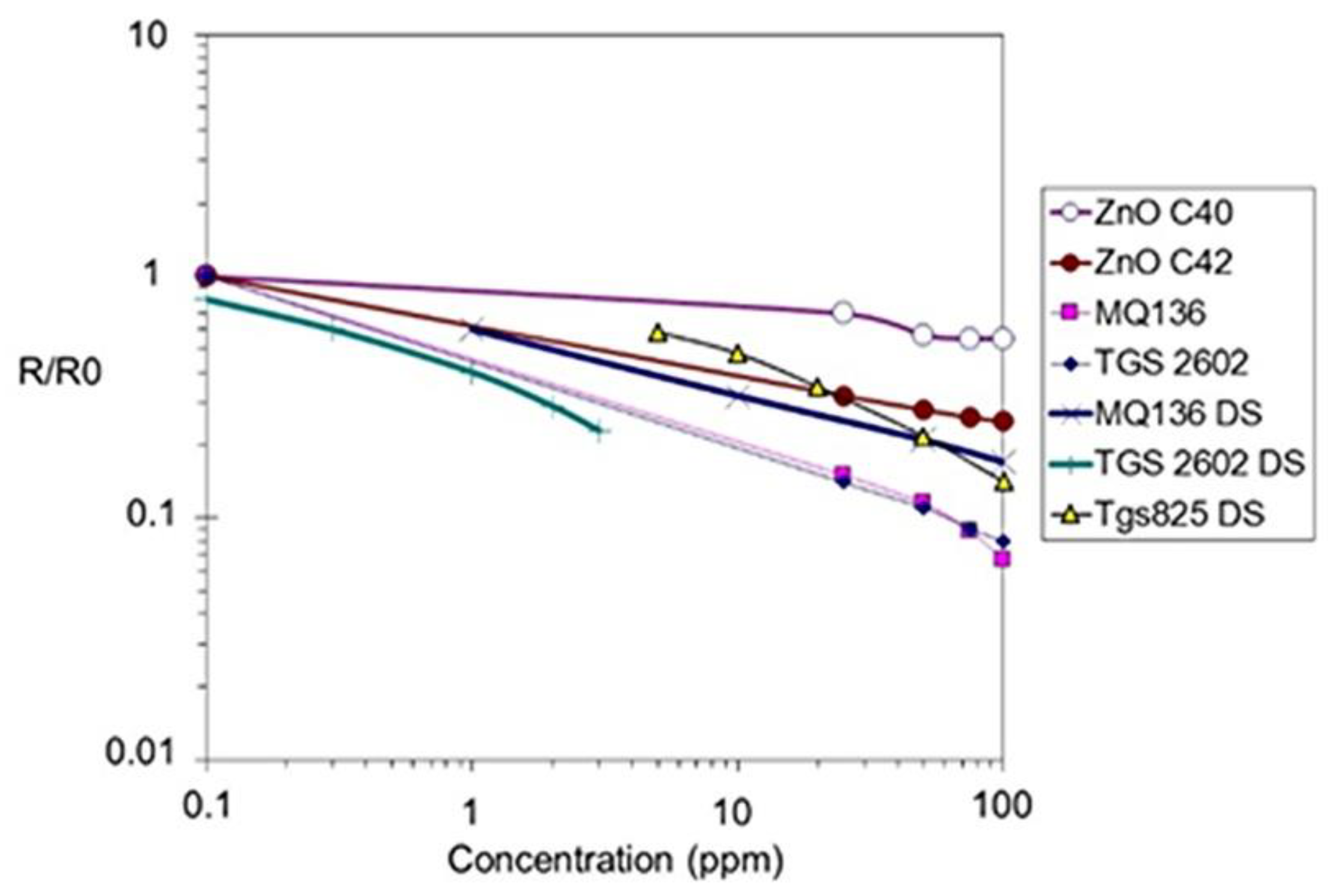
In a second step, the sensors made with ZnO C40 to C42 films were tested at the optimal temperature of 400 °C for different concentrations of H2S. Results on sensor C43 are not given because the sensor heater failed during this test. The concentration was adjusted from 25 to 100 ppm. Moreover, in view of comparing the performance of our homemade ZnO sensors, a challenging choice was made by testing current commercial semiconductor gas sensors in the same conditions. These conditions mean that all the gas sensors were tested with the same measurement setup, as defined in Figure 6, and with the same gas injection procedure. This comparison choice was preferred to a simple comparison to the literature because the literature samples are not tested in the same conditions, and generally, are not embedded in commercial cases for test under gas. The commercial sensors, i.e., MQ136 and TGS2602, from Zhengzhou Winsen Electronics Technology Co. (Zhengzhou, China), and Figaro USA Inc. (Arlington Heights, IL, USA), respectively, were tested by respecting the polarization conditions defined by the manufacturer. Additionally, for experimental measurements, data from technical datasheets were added as well, plotted in Figure 13. In these datasheets, the sensitivity is given by the relation:
where R is the measured resistance of the sensor under the test gas, R0 is the resistance in the initial conditions (under air, measurement temperature). So, all sensitivities were converted in the same form, defined by Equation (3).
S = R/R0
All the results on the sensitivity under different H2S concentrations are plotted in Figure 13. The average sensitivity of the ZnO sensors is really of interest, in particular for ZnO-C42, as no optimization of these first homemade gas sensors was performed. Actually, ZnO-C42 has a sensitivity of 0.25 at 100 ppm H2S. This value is not so far from the sensitivity value of commercial sensors, which was around 0.1 at 100 ppm H2S. So, we may expect to improve the ZnO sensor sensitivity by lowering the sensor volume and by optimizing the electrode configuration.
During the test of all these sensors, measurements of the dynamic response were also completed. The response time and recovery time values were extracted from dynamic responses under 100 ppm H2S, so from Figure 7, Figure 8, Figure 9, Figure 10 and Figure 11. All values have been given previously in Figure 12, with a discussion of these results. The dynamic responses of the commercial sensors have given a response time of 3–4 min. for TGS2602, and 2 min. for MQ136. In the literature, studies on ZnO films exposed to H2S generally display response time values ranging from 50 s to 5 min [28,29,30]. These results indicate that our ZnO sensors have similar response times or better in the case of ZnO-C42, and therefore confirm the great potential of our ZnO thin film-based gas sensors. In the future, a volume optimization of the gas sensor could be performed to improve the sensitivity value, as was shown with ZnO nanorods or nanowires [29,30].
4. Conclusions
In the continuously growing market of gas detection, there is an urgent need for lead-free components. So, we have decided to study the microstructure influence of zinc oxide thin films on the detection of hydrogen sulfide (H2S). Zinc oxide thin films were deposited by PLD on silicon substrates under different conditions to modify the microstructure, in particular the grain shape and size. Under an exposure of 100 ppm H2S, the sensors C41 and C42, composed of very small grains, have given a remarkable response value of 77% where S = (R0 − R)/R. Additionally, in view to compare our demonstrators to current commercial semiconductor gas sensors, measurements under H2S were also completed with sensors from Figaro and Winsen corporations. The H2S concentration was adjusted from 25 to 100 ppm. Sensitivity value as high as R/R0 = 0.25 was obtained at T = 400 °C under 100 ppm H2S. About the dynamic response, our best ZnO sensor has given better response times than commercial sensors with response times ranging from 30 to 50 s. All these results clearly demonstrate that ZnO thin films with a controlled microstructure could be of high interest for the development of highly sensitive commercial gas sensors.
Author Contributions
Conceptualization, D.F. and S.D.; methodology, D.F.; validation, D.F. and S.D.; formal analysis, D.F. and S.D.; investigation, D.F., S.D. and V.B.; resources, D.F.; data curation, D.F. and S.D.; writing—original draft preparation, D.F. and S.D.; writing—review and editing, D.F.; supervision, D.F. and M.G.-V.; project administration, D.F. and S.D.; funding acquisition, all authors. All authors have read and agreed to the published version of the manuscript.
Funding
This research was funded by the French Research Agency; grant number (ANR Ospégaz—ANR 11ECOT 01201-OSPEGAZ (oxydes sans plomb pour la détection de gaz). And The APC was funded by the University of Littoral Côte d’Opale (ULCO).
Institutional Review Board Statement
Not applicable.
Informed Consent Statement
Not applicable.
Acknowledgments
This study was supported by the French Research Agency (ANR Ospégaz—ANR 11ECOT 01201-OSPEGAZ (oxydes sans plomb pour la détection de gaz). The scanning electron microscopy was performed in ScanMAT UMS 20001 CNRS-University of Rennes 1, which received a financial support from the Région Bretagne, the Département d’Ile et Vilaine and the European Union (2015–2020 CPER projects SCANMAT and Verres). We also would like to thank Nicolas Uschanoff for his help during the measurements under gas conducted at Simtronics SAS.
Conflicts of Interest
The authors declare no conflict of interest.
References
- Fasquelle, D.; Députier, S.; Mascot, M.; Uschanoff, N.; Bouquet, V.; Demange, V.; Guilloux-Viry, M.; Carru, J.-C. Lead-free oxide thin films for gas detection. Adv. Mater. Res. 2013, 789, 105–111. [Google Scholar] [CrossRef]
- Fasquelle, D. Sensible Sensors. Int. Innov. Sci. Cycles 2014, 125, 106–108. [Google Scholar]
- Barsan, N.; Koziej, D.; Weimar, U. Metal oxide-based gas sensor research: How to? Sens. Actuators B 2007, 121, 18–35. [Google Scholar] [CrossRef]
- Korotcenkov, G. Metal oxides for solid-state gas sensors: What determines our choice? Mater. Sci. Eng. B 2007, 139, 1–23. [Google Scholar] [CrossRef]
- Fasquelle, D.; Verbrugghe, N.; Députier, S. Tungsten-Based Cost-Effective Gas Sensors for H2S Detection. Chemosensors 2021, 9, 295. [Google Scholar] [CrossRef]
- Gas’kov, A.M.; Rumyantseva, M.N. Materials for Solid-State Gas Sensors. Inorg. Mater. 2000, 36, 293–301. [Google Scholar] [CrossRef]
- Marikutsa, A.; Rumyantseva, M.; Gaskov, A. Selectivity of Catalytically Modified Tin Dioxide to CO and NH3 Gas Mixtures. Chemosensors 2015, 3, 241–252. [Google Scholar] [CrossRef] [Green Version]
- Vorobyeva, N.; Rumyantseva, M.; Filatova, D.; Konstantinova, E.; Grishina, D.; Abakumov, A.; Turner, S.; Gaskov, A. Nanocrystalline ZnO(Ga): Paramagnetic centers, surface acidity and gas sensor properties. Sens. Actuators B 2013, 182, 555–564. [Google Scholar] [CrossRef]
- Kanan, S.M.; El-Kadri, O.M.; Abu-Yousef, I.A.; Kanan, M.C. Semiconducting Metal Oxide Based Sensors for Selective Gas Pollutant Detection. Sensors 2009, 9, 8158–8196. [Google Scholar] [CrossRef] [Green Version]
- Bochenkov, V.E.; Sergeev, G.B. Sensitivity, Selectivity, and Stability of Gas-Sensitive Metal-Oxide Nanostructures, Metal Oxide Nanostructures and Their Applications; American Scientific Publishers: Moscow, Russian, 2010; Volume 3, pp. 31–52. [Google Scholar]
- Chakraborty, S.; Sen, A.; Maiti, H.S. Selective detection of methane and butane by temperature modulation in iron doped tin oxide sensors. Sens. Actuators B 2006, 115, 610. [Google Scholar] [CrossRef]
- Parret, F.; Ménini, P.; Martinez, A.; Soulantica, K.; Maisonnat, A.; Chaudret, B. Improvement of micromachined SnO2 gas sensors selectivity by optimised dynamic temperature operating mode. Sens. Actuators B 2006, 118, 276. [Google Scholar] [CrossRef]
- Nakata, S.; Okunishi, H.; Nakashima, Y. Distinction of gases with a semiconductor sensor under a cyclic temperature modulation with second-harmonic heating. Sens. Actuators B 2006, 119, 556. [Google Scholar] [CrossRef]
- Huang, J.R.; Li, C.Y.; Huang, Z.Y.; Huang, X.J.; Liu, J.H. Temperature modulation and artificial neural network evaluation for improving the CO selectivity of SnO2 gas sensor. Sens. Actuators B 2006, 114, 1059. [Google Scholar] [CrossRef]
- Huang, J.R.; Gu, C.P.; Meng, F.L.; Li, M.Q.; Liu, J.H. Detection of volatile organic compounds by using a single temperature-modulated SnO2 gas sensor and artificial neural network. Smart Mater. Struct. 2007, 16, 701. [Google Scholar] [CrossRef]
- Sysoev, V.V.; Goschnick, J.; Schneider, T.; Strelcov, E.; Kolmakov, A. A Gradient Microarray Electronic Nose Based on Percolating SnO2 Nanowire Sensing Elements. Nano Lett. 2007, 7, 3182. [Google Scholar] [CrossRef] [PubMed]
- Röck, F.; Barsan, N.; Weimar, U. Electronic Nose: Current Status and Future Trends. Chem. Rev. 2008, 108, 705. [Google Scholar] [CrossRef]
- MQ136 Technical Datasheet; Winsen Corp.: Zhengzhou, China, 2015.
- TGS 2602 Technical Datasheet; Figaro USA, Inc.: Arlington Heights, IL, USA, 2017.
- TGS 825 Technical Datasheet; Figaro USA, Inc.: Arlington Heights, IL, USA, 2013.
- Pati, S.; Banerji, P.; Majumder, S.B. MOCVD grown ZnO thin film gas sensors: Influence of microstructure. Sens. Actuators A 2014, 213, 52–58. [Google Scholar] [CrossRef]
- Bao, D.; Gu, H.; Kuang, A. Sol-gel-derived c-axis oriented ZnO thin films. Thin Solid Film 1998, 312, 37–39. [Google Scholar] [CrossRef]
- Bouderbala, M.; Hamzaoui, S.; Amrani, B.; Reshak, A.H.; Adnane, M.; Sahraoui, T.; Zerdali, M. Thickness dependence of structural, electrical and opticalbehaviour of undoped ZnO thin films. Phys. B 2008, 403, 3326–3330. [Google Scholar] [CrossRef]
- Wang, Y.; Kang, K.-M.; Kim, M.; Park, H.-H. Film thickness effect in c-axis oxygen vacancy-passivated ZnO prepared via atomic layer deposition by using H2O2. Appl. Surf. Sci. 2020, 529, 147095. [Google Scholar] [CrossRef]
- Amirhaghi, S.; Craciun, V.; Craciun, D.; Elder, J.; Boyd, I.W. Low temperature growth of highly transparent c-axis oriented ZnO thin films by pulsed laser deposition. Microelectron. Eng. 1994, 25, 32l–326. [Google Scholar] [CrossRef] [Green Version]
- Zerdali, M.; Hamzaoui, S.; Teherani, F.H.; Rogers, D. Growth of ZnO thin film on SiO2/Si substrate by pulsed laser deposition and study of their physical properties. Mater. Lett. 2006, 60, 504–508. [Google Scholar] [CrossRef]
- Carpenter, M.A.; Mathur, S.; Kolmakov, A. Metal. Oxide Nanomaterials for Chemical Sensors; Springer: Berlin/Heidelberg, Germany, 2013; p. 548. ISBN 978-1-4614-5394-9. [Google Scholar]
- Kalyamwar, V.S.; Raghuwanshi, F.C.; Jadhao, N.L.; Gadewar, A.J. Zinc Oxide Nanostructure Thick Films as H2S Gas Sensors at Room Temperature. J. Sens. Technol. 2013, 3, 31–35. [Google Scholar] [CrossRef] [Green Version]
- Bhati, V.S.; Hojamberdiev, M.; Kumar, M. Enhanced sensing performance of ZnO nanostructures-based gas sensors: A review. Energy Rep. 2020, 6, 46–62. [Google Scholar] [CrossRef]
- Comini, E.; Baratto, C.; Faglia, G.; Ferroni, M.; Vomiero, A.; Sberveglieri, G. Quasi-one dimensional metal oxide semiconductors: Preparation, characterization and application as chemical sensors. Prog. Mater. Sci. 2009, 54, 1–67. [Google Scholar] [CrossRef]
Figure 1.
θ-2θ XRD patterns of ZnO/Si (100) thin films deposited under different conditions of temperature and pressure.
Figure 1.
θ-2θ XRD patterns of ZnO/Si (100) thin films deposited under different conditions of temperature and pressure.

Figure 2.
FE-SEM images of the surface morphology (on the top) and cross-section (at the bottom) of ZnO thin films under various deposition conditions. All the images are at the same scale, indicated in the top left one.
Figure 2.
FE-SEM images of the surface morphology (on the top) and cross-section (at the bottom) of ZnO thin films under various deposition conditions. All the images are at the same scale, indicated in the top left one.

Figure 3.
FE-SEM images showing the microstructure of the ZnO thin films deposited by PLD on SiO2/Si substrates under different conditions. The inset of C41 illustrated the columnar growth of the films.
Figure 3.
FE-SEM images showing the microstructure of the ZnO thin films deposited by PLD on SiO2/Si substrates under different conditions. The inset of C41 illustrated the columnar growth of the films.

Figure 4.
Resistance of sensors in function of frequency.

Figure 5.
Semiconductor gas sensor. On the left: schematic; center: wiring of electrodes; on the right: commercial case used for measurements under gas.
Figure 5.
Semiconductor gas sensor. On the left: schematic; center: wiring of electrodes; on the right: commercial case used for measurements under gas.

Figure 6.
On the left: sensor and e-card for signal conditioning. On the right: measurement set-up.

Figure 7.
Response of sensor C39 under 100 ppm H2S at T = 400 °C.

Figure 8.
Response of sensor C40 under 100 ppm H2S at T = 400 °C.

Figure 9.
Response of sensor C41 under 100 ppm H2S at T = 400 °C.

Figure 10.
Response of sensor C42 under 100 ppm H2S at T = 400 °C.

Figure 11.
Response of sensor C43 under 100 ppm H2S at T = 400 °C.

Figure 12.
Summary of the response parameters of the sensors C39 to C43 under 100 ppm H2S at T = 400 °C.
Figure 12.
Summary of the response parameters of the sensors C39 to C43 under 100 ppm H2S at T = 400 °C.

Figure 13.
Sensitivity of two ZnO gas sensors, C40 and C42, compared to commercial sensors. For commercial sensors, experimental data and data extracted from technical datasheet (noted DS) are given.
Figure 13.
Sensitivity of two ZnO gas sensors, C40 and C42, compared to commercial sensors. For commercial sensors, experimental data and data extracted from technical datasheet (noted DS) are given.


Table 1.
Conditions of deposition, XRD analyses, film thickness, and electrical resistance of ZnO/Si (100) thin films.
Table 1.
Conditions of deposition, XRD analyses, film thickness, and electrical resistance of ZnO/Si (100) thin films.
| Sample | C10 | C9 | C12 | C15 | C11 | C14 | C22 |
|---|---|---|---|---|---|---|---|
| Temperature (°C) | 350 | 350 | 350 | 700 | 700 | 700 | 700 |
| Pressure (mbar) | vacuum | 0.06 | 0.7 | vacuum | 0.06 | 0.7 | 1 |
| Deposition duration (min) | 30 | 30 | 15 | 15 | 15 | 10 | 10 |
| (002) diffraction peak position (°2θ) | 34.033 | 34.372 | 34.475 | 34.451 | 34.583 | 34.469 | 34.471 |
| c parameter (Å) | 5.264 | 5.214 | 5.199 | 5.202 | 5.183 | 5.200 | 5.199 |
| FWHM (002) (°) | 0.893 | 0.130 | 0.290 | 0.124 | 0.102 | 0.115 | 0.113 |
| Crystallite size D (Å) | 93 | 694 | 289 | 734 | 932 | 800 | 817 |
| Film thickness (nm) | 700 | 700 | 500 | 200 | 400 | 500 | 600 |
| Sheet resistance | 1 kΩ | 10 kΩ | 100 kΩ | 10 kΩ | 400 kΩ | 10 MΩ | 10 MΩ |
Table 2.
Deposition parameters of C39 to C43 labeled films.
| Sample | C39 | C40 | C41 | C42 | C43 | |
|---|---|---|---|---|---|---|
| Deposition conditions | Laser frequency (Hz) | 5 | 5 | 4 | 4 | 4 |
| T (°C) | 350 | 700 | 700 | 700 | 700 | |
| p (mbar) | 0.7 | 0.7 | 1 | 0.7 | 0.3 | |
| Substrate-target distance (mm) | 42 | 42 | 42 | 34 | 34 | |
| Duration (min) | 15 | 10 | 10 | 20 | 20 | |
Publisher’s Note: MDPI stays neutral with regard to jurisdictional claims in published maps and institutional affiliations. |
© 2022 by the authors. Licensee MDPI, Basel, Switzerland. This article is an open access article distributed under the terms and conditions of the Creative Commons Attribution (CC BY) license (https://creativecommons.org/licenses/by/4.0/).
Share and Cite
MDPI and ACS Style
Fasquelle, D.; Députier, S.; Bouquet, V.; Guilloux-Viry, M. Effect of the Microstructure of ZnO Thin Films Prepared by PLD on Their Performance as Toxic Gas Sensors. Chemosensors 2022, 10, 285. https://doi.org/10.3390/chemosensors10070285
AMA Style
Fasquelle D, Députier S, Bouquet V, Guilloux-Viry M. Effect of the Microstructure of ZnO Thin Films Prepared by PLD on Their Performance as Toxic Gas Sensors. Chemosensors. 2022; 10(7):285. https://doi.org/10.3390/chemosensors10070285
Chicago/Turabian StyleFasquelle, Didier, Stéphanie Députier, Valérie Bouquet, and Maryline Guilloux-Viry. 2022. "Effect of the Microstructure of ZnO Thin Films Prepared by PLD on Their Performance as Toxic Gas Sensors" Chemosensors 10, no. 7: 285. https://doi.org/10.3390/chemosensors10070285
Note that from the first issue of 2016, this journal uses article numbers instead of page numbers. See further details here.