Reflection Enhancement and Giant Lateral Shift in Defective Photonic Crystals with Graphene


School of Electronic and Information Engineering, Hubei University of Science and Technology, Xianning 437100, China
*
Authors to whom correspondence should be addressed.
†
These authors contributed equally to this work.
Appl. Sci. 2019, 9(10), 2141; https://doi.org/10.3390/app9102141
Submission received: 24 April 2019
/
Revised: 9 May 2019
/
Accepted: 14 May 2019
/
Published: 25 May 2019
(This article belongs to the Special Issue Novel Advances in Optical Micro- and Nano-Cavities)
Abstract
:Featured Application
highly sensitive sensor.
Abstract
This study investigates the reflectance of the defective mode (DM) and the lateral shift of reflected beam in defective photonic crystals incorporated with single-layer graphene by the transfer matrix method (TMM). Graphene, treated as an equivalent dielectric with a thickness of 0.34 nm, was embedded in the center of a defect layer. The reflectance of the DM was greatly enhanced as the intraband transition of electrons was converted to an interband transition in graphene. The reflectance of the DM could be further enhanced by increasing the Bragg periodic number. Furthermore, a large lateral shift of the reflected beam could also be induced around the DM. This study may find great applications in highly sensitive sensors.
1. Introduction
It is well known that the most typical property of photonic crystals (PCs) is the photonic bandgap structure [1]. As a light beam impinges upon PCs, there is a large lateral shift of the reflected beam on the bandgap edge [2]. The shift of reflected beam, which can be spatial and angular, was firstly confirmed experimentally by Goos and Hänchen [3]. The spatial shift and angular deviation from the prediction of geometrical optics essentially result from the dispersion of reflection coefficients, and could be estimated by the famous Artmann formula [4]. Giant lateral shift has also been reported inside the reflection band, and become extremely large at exceptional points (EPs) in parity–time-symmetric (PT-symmetric) PCs [5]. Furthermore, a great lateral shift may also exist in non-Hermitian systems and periodic dielectric multilayers with PT-symmetry [6,7]. Meanwhile, low loss in slabs and defects embedded in PCs can greatly enhance the lateral shift [8,9]. The defective mode (DM) locates at the middle of the bandgap in defective PCs. The lateral shift of the reflected beam near the DM is generally dozens of incident wavelengths, and the reflectivity of the DM can be as low as zero in passive PCs. On the other hand, non-Hermitian systems can induce many unique optical phenomena, and have become a hot topic in optics and other fields [10,11,12,13,14,15,16,17]. In non-Hermitian systems, large lateral shift can be obtained near exceptional point (EP) and coherent-perfect-absorption (CPA)-laser state [5,6,18], but the reflectivity of the EP is also zero and the reflectivity is very low near it [19,20,21] while the CPA-laser state is unstable, so these are not conducive to the observation of lateral shift for reflected beams.
Graphene is an ultrathin two-dimensional material, and it has been studied intensively for its fascinating optical, electronic, and mechanical properties [22,23,24,25,26]. The surface conductivity of graphene could be flexibly modulated by chemical doping or external gate voltages, and the low loss in graphene exists across a wide frequency range [27,28]. Therefore, we constructed a complex system composed of graphene and defective PCs, of which the surface current of graphene could be utilized to enhance the reflectance of the DM and a giant lateral shift could be induced to obtain low loss in graphene.
In this study, we investigated the enhancement of reflectance and the lateral shift of reflected beams in defective PCs incorporated with graphene. Graphene was embedded in the PCs to enhance the reflectance of the DM by utilizing the transition conversion of electrons in graphene. Subsequently, we calculated the reflection of the DM for different Bragg periodic numbers. Finally, we studied the lateral shift of reflected beams around the DM as well as the tunability of the lateral shift.
2. One-Dimensional Defective PCs
Figure 1 shows a schematic of the one-dimensional defective PCs. The dielectrics A and B were arranged alternatively on both sides of the defect layer C, forming two Bragg gratings. The defective system could also be viewed as a Fabry–Pérot resonant cavity, in which the Bragg gratings are two reflectors and the defect layer plays the role of cavity. A single-layer graphene was embedded in the center of the defect layer. The thickness of dielectrics A and B was λ0/4n, where λ0 = 1.55 μm denotes the midgap (resonant) wavelength of the defective periodic multilayers. The thickness of the defect layer C was λ0/2n. The refractive indices of dielectric were na = 1.38 and nb = nc = 2.35, respectively.
Graphene is a two-dimensional material, and we treated it as an equivalent dielectric with a thickness of dg = 0.34 nm [29,30]. The surface conductivity of graphene can be modulated by chemical doping or gate voltages, so the type of graphene can be doped or pure. Subsequently, the relative equivalent permittivity of graphene can be given by εg = 1 + iσgη0/(kdg) [28], where k = 2π/λ is the wave number of incident light in vacuum, η0 is the vacuum resistivity, and σg is the total surface conductivity of graphene. The parameter σg can be written as σg = σ(1) + σ(3)|Ez|2, where σ1 is the linear surface conductivity of graphene and σ(3) is the nonlinear coefficient of surface conductivity. Here we assumed that the input intensity of light was low enough and ignored the nonlinear effect of graphene. The linear surface conductivity is governed by the Kubo formula [27,31], which depends on the incident wavelength λ, chemical potential μ, absolute temperature T, and momentum relaxation time τ. We chose the incident wavelength around λ0, and set τ = 0.5 ps, T = 300 K in the following study. As a light beam impinges upon the system, the reflection and transmission coefficients are denoted by r and t, respectively. The two coefficients could be obtained by the transfer matrix method (TMM) [32]. The transmittance T is identified as T = tt * = It/Ii, where It and Ii are the transmitted and incident intensities, respectively. The reflectance R is identified as R = rr *.
3. Reflectance Enhanced with Graphene
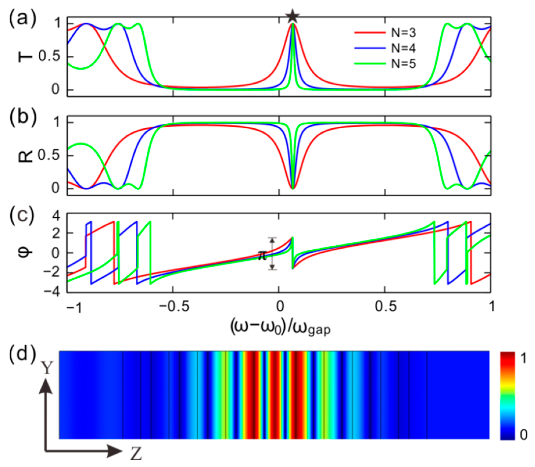
Now we calculate the transmission and reflection spectra as the TM wave obliquely impinges upon the defective PCs incorporated without graphene. The incident angle is θ = 20°. Figure 2a shows the transmittance spectra for three different Bragg periodic numbers N = 3, 4, and 5, respectively. The transmittance varies with the normalized frequency (ω − ω0)/ωgap, where the photonic bandgap of PCs is ωgap = 4ω0arcsin|(nb − na)/(nb + na)|2/π [1], and ω0 = 2πc/λ0 is the center frequency of the bandgap.
There was a peak in each spectrum near the zero point of normalized frequency. The maximum value Tm = 1 at the spectrum center (ω − ω0)/ωgap = 0.065 corresponds to the transmittance of the DM, denoted by a star symbol. The transmission spectrum width was smaller for a larger Bragg periodic number N, demonstrating its good frequency selectivity. Figure 2b shows the reflectance spectrum. The reflectances of the DM were all as low as zero for the three Bragg periodic numbers. This shows that there was no light reflected from the PCs, as the incident frequency identified with the DM. The PCs became transparent for this specific frequency wave, so the DM is also known as a transmission mode. Figure 2c shows the phase of the reflection coefficient. The phase varied with the normalized frequency. There was a π phase hopping at the DM in each phase curve for different Bragg periodic numbers. The reflectance was zero at the DM, which resulted in uncertainty in the phase of the reflection coefficient. Figure 2d shows the distribution of the DM. It illustrates that the electric field was mainly localized at the defect layer, and the electric field exponentially decayed as it departed from the center along the z-axis.
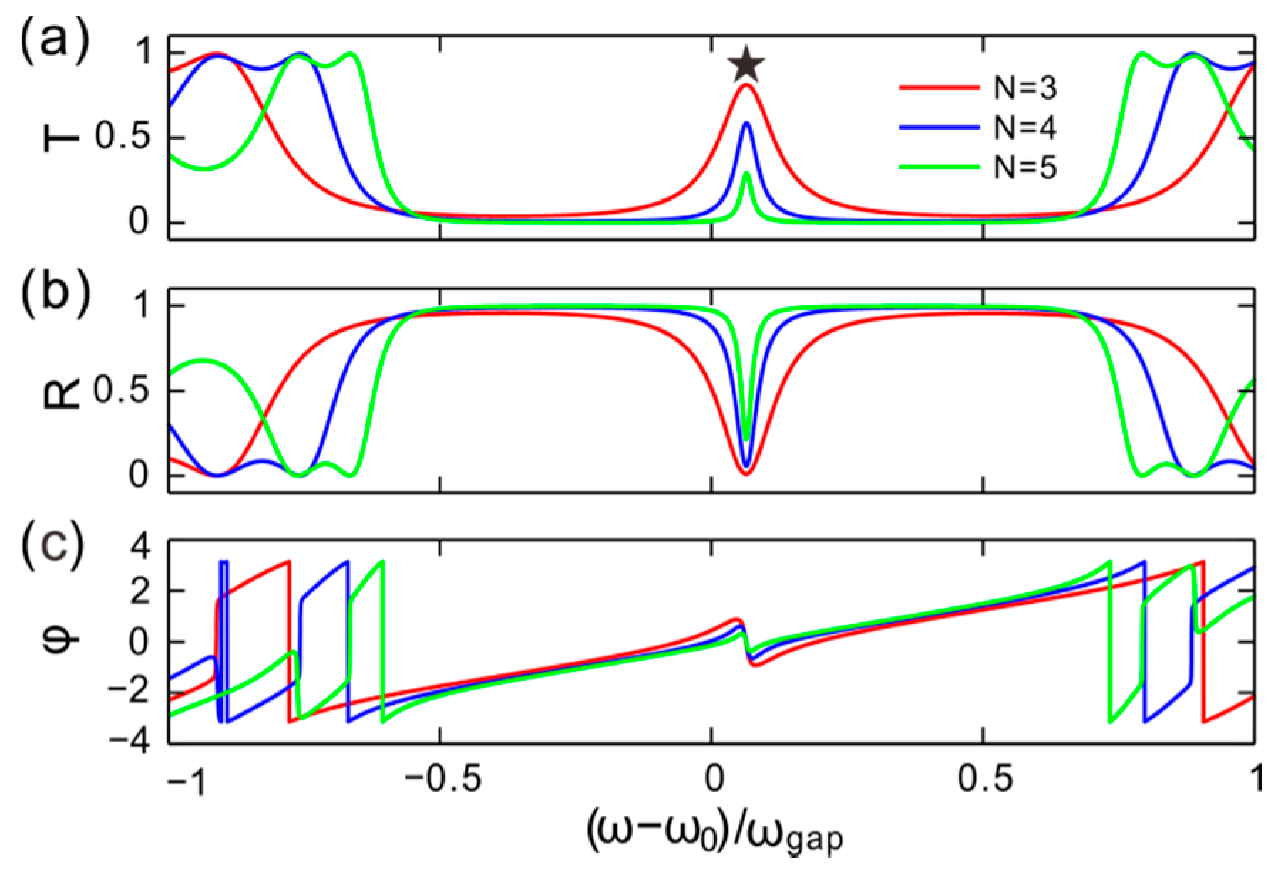
We embedded single-layer graphene in the middle of the defect and investigated the influence on transmittance, reflectance, and phase of the reflection coefficient with the interaction between the graphene and the electric field of the DM. Figure 3a shows the transmittance spectra. One can find that the transmittance of the DM was no longer constant, and decreased with the increase of the Bragg periodic number N. On the contrary, the reflectance of the DM increased with the Bragg periodic number, as shown in Figure 3b. In other words, the reflection intensity of light could be greatly enhanced by increasing N.
The reflection coefficient is represented by r = |r|exp(iφ), where φ is the phase change of the reflected beam. The graphene inset at the defect therefore apparently influenced the reflection behavior of light—especially the reflection phase. Figure 3c shows that the reflection phase varied continuously with the normalized frequency, but did not change abruptly at the DM. As the frequency increased, the phase changed dramatically around the DM. This behavior indicates that a large lateral shift of the reflected beam may have been induced, since the lateral shift was proportional to the curvature of the phase curve.
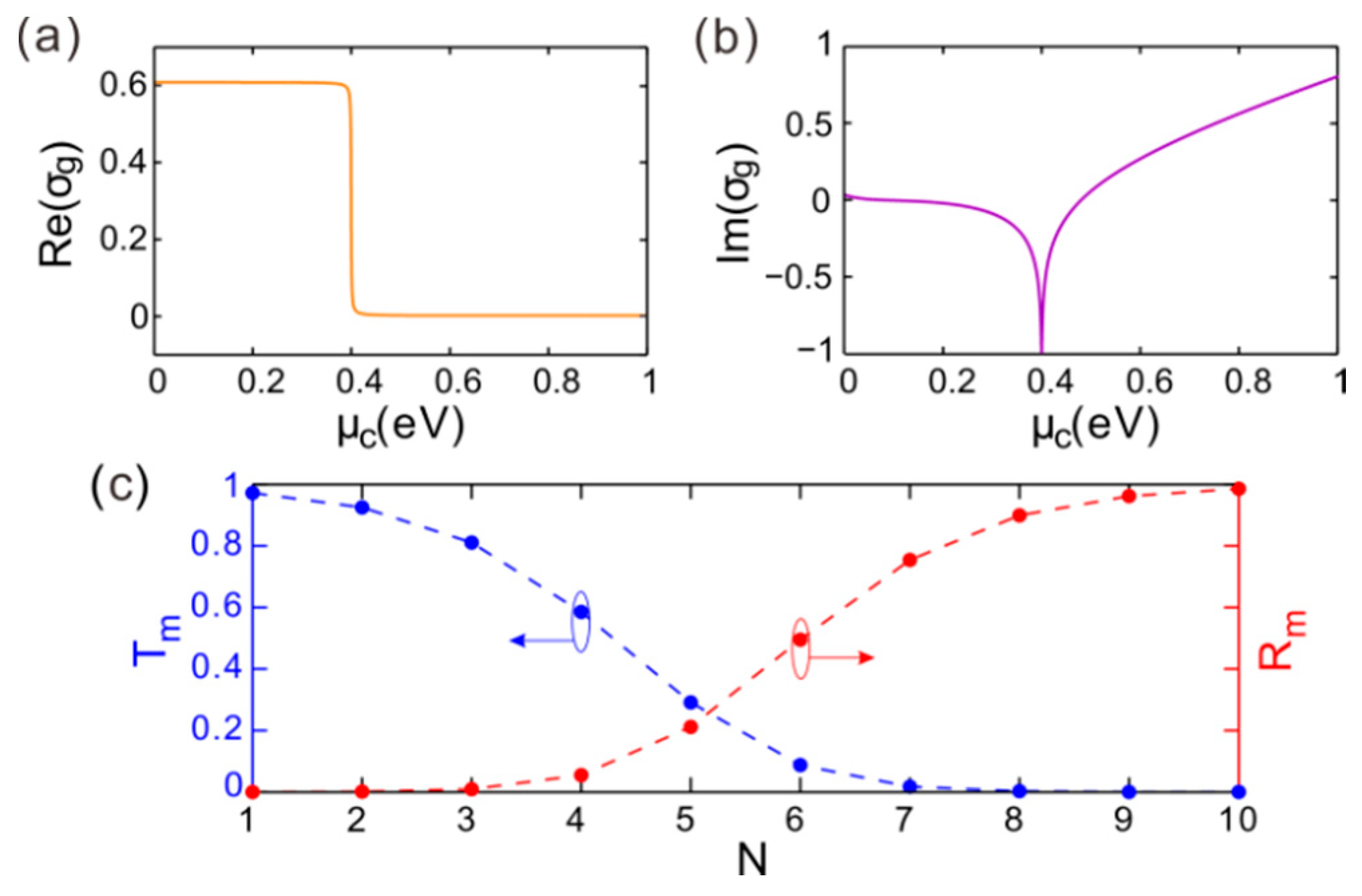
The surface conductivity is a function of the chemical potential of graphene, so the optical properties can be readily modulated by the chemical potential. Figure 4a shows the transmittance of light in the parameter space composed of the normalized frequency and the chemical potential of graphene. We took the logarithm log10R for increasing image contrast. One can see that the transmittance was a function of these two parameters. As the chemical potential increased, the transmittance varied with the normalized frequency. For a fixed chemical potential, there was a maximum in each transmission spectrum. The maximum corresponded to the transmittance of the DM. This demonstrates that the frequency of the DM remained approximately constant as the chemical potential changed, while the transmittance changed abruptly near μc = 0.41 eV. The transmission mode (i.e., the DM) corresponded to the maximum of transmission spectrum in the middle of the bandgap.
Figure 4b shows the transmittance of the DM for different chemical potential. It shows that the maximum was Tm = 0.29 when the chemical potential μc < 0.41 eV, and the maximum was Tm = 0.99 when the chemical potential μc > 0.41 eV. Figure 4c shows the reflectance of light. It demonstrates that the position of minimum reflectance goes along with the DM in the parameter space as the chemical potential changed. Figure 4d shows the minimum reflectance in the bandgap. It shows the maximum changed with the chemical potential of graphene. The value was Rm = 0.21 when the chemical potential μc < 0.41 eV, and the minimum was Rm = 0 when the chemical potential μc > 0.41 eV. The surface conductivity of graphene is contributed by electron movement. The intraband transition of electron movement governs mainly for a low chemical potential, while the interband transition plays a leading role for a high chemical potential [24,31].
Figure 5a shows the real part of the surface conductivity of graphene. It varied with the chemical potential of graphene. As μc < 0.41 eV, the real part of the surface conductivity of graphene was close to 0.6 S. High surface conductivity corresponds to a strong surface current, which can induce reflection enhancement in the DM. The real part of the surface conductivity of graphene was close to zero as μc > 0.41 eV, in which the graphene presented complete transparency. Figure 5b shows the imaginary part of the surface conductivity of graphene. There was a minimum in the imaginary part curve as the chemical potential changed. The imaginary part of the surface conductivity is equivalent to the real part of the refractive index if we regard the graphene as an equivalent dielectric. Therefore, the center frequency of DM may vary with the chemical potential of graphene. Furthermore, the periodic structure of the system can also influence the reflectance of the DM, as shown in Figure 5c. The chemical potential took a fixed value of μc = 0.15 eV. One can see that the reflectance of DM increased with the increase of the Bragg periodic number N, while the transmittance of the DM decreased. The resonance of the DM was stronger for larger N. The enhancement of the local field where the graphene was located contributed to the interband transition of electrons as the Bragg number N increased.
4. Large Lateral Shift around the DM
Figure 6a shows the phase of the reflection coefficient. For each fixed chemical potential, there is a corresponding phase curve. The phase varied with the normalized frequency. The change in phase became particularly dramatic in the area around the DM. Especially, the phase approximated a step change at the DM as the chemical potential μc > 0.41 eV. To demonstrate the details of the phase change, Figure 6b depicts the phase curve for three different chemical potentials: μc = 0.25, 0.41, and 0.60 eV. One can see that the phase varied with the normalized frequency. Around the DM, the curvature was negative, but it became positive as the frequency extended to both sides beyond the DM. The interval of phase change at the DM enlarged as the chemical potential increased and the change in phase approached π; even so, the phase curve still varied continuously and there was no hopping in phase. This means that a higher chemical potential may lead to a greater change in the phase of the reflection coefficient around the DM. The loss of graphene decreased greatly as the chemical potential exceeded 0.41 eV. Low loss in materials can induce a sharp change in the reflection coefficient phase [6].
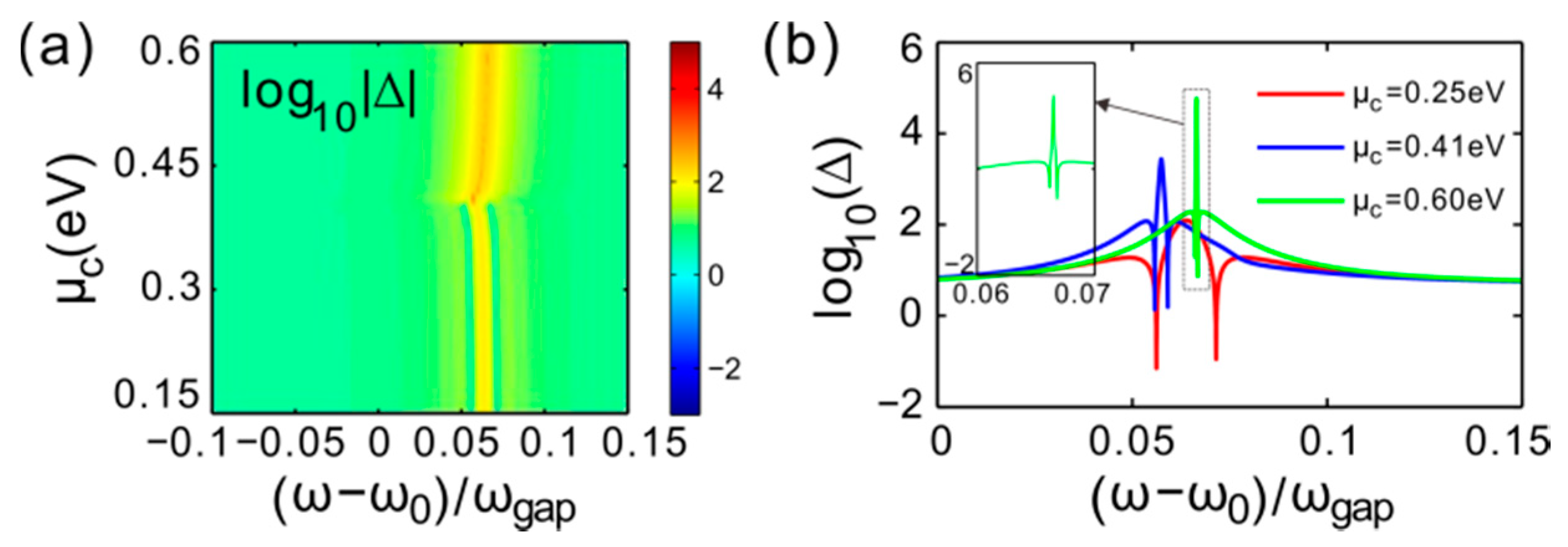
As an incident beam impinges upon the structure, the lateral shift of the reflected beam can be derived by Δ = −dφ/dk [33]. Figure 7a shows the lateral shift in the parameter space composed of the chemical potential and normalized frequency. For each fixed chemical potential, the lateral shift of the reflected beam can be positive or negative as the normalized frequency changes, and the extrema are very large. Therefore, for better contrast, we took the logarithm of the absolute lateral shift (i.e., log10|Δ|). One can see that the lateral shift was large in the region around the DM in the parameter space. There was an obvious difference in the lateral shift near the chemical potential μc = 0.41 eV.
Figure 7b shows the lateral shift of the reflected beam for different chemical potential. The lateral shift is a function of the normalized frequency. There was a peak and two valleys in each curve of lateral shift. The extrema were Δ = 124λ, −18.8λ, and −18.9λ for μc = 0.25 eV. The extrema were Δ = 2.74 × 10³λ, −118.6λ, and −117.4λ for μc = 0.41 eV. The extrema were Δ = 5.74 × 10⁴λ, −118.9λ, and −119λ for μc = 0.60 eV. Therefore, by increasing the frequency, the peak in the shift curve became sharper and the gap between the two valleys reduced. This super-sensitive lateral shift effect of reflected beam could be used for the detection of weak physical effects [34,35]. The surface conductivity of graphene is a function of the chemical potential and normalized frequency. The loss is lower for larger chemical potential. Low loss can cause violent fluctuation in phase of reflection coefficient around the DM as the normalized frequency changes, and then the dramatic fluctuation in phase induces large lateral shift of reflected beam. We only used TM waves as the typical incident beam in the present study. In fact, when TE waves were used for calculation, similar results were obtained. When the structure is fixed, the reflection spectrum is a function of incident angle and incident wavelength. Different incident angles only affect the location of the defect mode, but the reflectivity enhancement and giant lateral shift near the defect mode are not affected. Here, we selected the incident angle of 20°, which has no special meaning—it is just a typical example to illustrate our simulation results. The conductivity of multilayer graphene can be described by σml = σgNgra as Ngra < 7, where Ngra is the number of graphene layers [36]. Subsequently, the relative equivalent permittivity of multilayer graphene could be given by εml = 1 + iσmlη0/(kNgradg) = 1 + iσgη0/(kdg), which is equal to the equivalent permittivity of single-layer graphene εg. We simulated the cases of double and multilayer graphene, and results showed that the main conclusion was not affected by the number of layers.
5. Conclusions
We studied the reflectance of DM and the lateral shift of the reflected beam in defective PCs with graphene embedded in the center of the defect layer. High reflectivity of the DM and giant lateral shift near the DM were realized simultaneously. The interband transition of electrons in graphene greatly enhanced the reflection of the DM, and its reflectance could be as high as 0.21 for the Bragg periodic number N = 5. The reflectance could be further enhanced by increasing the number N. Meanwhile, large lateral shift of the reflected beam was induced, and the shift could be positive or negative. The maximum of lateral shift approached the magnitude of 104λ around the DM. The lateral shift could also be tuned by the chemical potential of graphene. This study paves the way for the development of highly sensitive sensors.
Author Contributions
Software, F.L. and J.W.; investigation, D.Z. (Dong Zhao) and D.Z. (Dong Zhong); writing—original draft preparation, D.Z. (Dong Zhao); writing—review and editing, D.Z. (Dong Zhao), P.M., S.X. and D.Z. (Dong Zhong); funding acquisition, Z.L. and D.Z. (Dong Zhao).
Funding
National Natural Science Foundation of China (NSFC) (61575148); Natural Science Foundation of Hubei Province (2015CFA040, 2016CFB515); Educational Commission of Hubei Province (D20172803); Humanities and Social Science Project of Hubei Education Department (18Q164); Colleges and Universities of National Innovation and Entrepreneurship Training Plan (201710927006Z, 201810927011).
Conflicts of Interest
The authors declare no conflicts of interest.
References
- Yariv, A.; Yeh, P. Photonics: Optical Electronics in Modern Communications, 6th ed.; Oxford University Press: New York, NY, USA, 2007. [Google Scholar]
- Felbacq, D.; Moreau, A.; Smaâli, R. Goos-Hänchen effect in the gaps of photonic crystals. Opt. Lett. 2003, 28, 1633–1635. [Google Scholar] [CrossRef] [PubMed]
- Goos, F.; Hänchen, H. A new and fundamental experiment on total reflection. Ann. Phys. 1947, 1, 333. [Google Scholar] [CrossRef]
- Aiello, A.; Woerdman, J.P. Role of beam propagation in Goos-Hänchen and Imbert-Fedorov shifts. Opt. Lett. 2008, 33, 1437–1439. [Google Scholar] [CrossRef] [PubMed]
- Longhi, S.; della Valle, G.; Staliunas, K. Goos-Hänchen shift in complex crystals. Phys. Rev. A 2011, 84, 042119. [Google Scholar] [CrossRef]
- Ma, P.; Gao, L. Large and tunable lateral shifts in one-dimensional PT-symmetric layered structures. Opt. Express 2017, 25, 9676–9688. [Google Scholar] [CrossRef]
- Zhao, D.; Ke, S.; Liu, Q.; Wang, B.; Lu, P. Giant Goos-Hänchen shifts in non-Hermitian dielectric multilayers incorporated with graphene. Opt. Express 2018, 26, 2817–2828. [Google Scholar] [CrossRef]
- Wang, L.G.; Chen, H.; Zhu, S.Y. Large negative goos-hänchen shift from a weakly absorbing dielectric slab. Opt. Lett. 2005, 30, 2936–2938. [Google Scholar] [CrossRef]
- Wang, L.G.; Zhu, S.Y. Giant lateral shift of a light beam at the defect mode in one-dimensional photonic crystals. Opt. Lett. 2006, 31, 101–103. [Google Scholar] [CrossRef]
- Ke, S.; Liu, J.; Liu, Q.; Zhao, D.; Liu, W. Strong absorption near exceptional points in plasmonic wave guide arrays. Opt. Quant. Electron. 2018, 50, 318. [Google Scholar] [CrossRef]
- Li, M.; Xie, H.; Cao, W.; Luo, S.; Tan, J.; Feng, Y.; Du, B.; Zhang, W.; Li, Y.; Zhang, Q.; et al. Photoelectron holographic interferometry to probe the longitudinal momentum offset at the tunnel exit. Phys. Rev. Lett. 2019, 122, 183202. [Google Scholar] [CrossRef]
- He, Y.; He, L.; Lan, P.; Wang, B.; Li, L.; Zhu, X.; Cao, W.; Lu, P. Molecular rotation movie filmed with high-harmonic generation. arXiv 2019, arXiv:1902.05662. [Google Scholar]
- Ke, S.; Zhao, D.; Liu, Q.; Liu, W. Adiabatic transfer of surface plasmons in non-Hermitian graphene waveguides. Opt. Quant. Electron. 2018, 50, 393. [Google Scholar] [CrossRef]
- Ke, S.; Zhao, D.; Liu, Q.; Wu, S.; Wang, B.; Lu, P. Optical imaginary directional couplers. J. Lightwave Technol. 2018, 36, 2510–2515. [Google Scholar] [CrossRef]
- Xu, S.L.; Zhao, Y.; Petrović, N.Z.; Belić, M.R. Spatiotemporal soliton supported by parity-time symmetric potential with competing nonlinearities. EPL 2016, 115, 14006. [Google Scholar] [CrossRef]
- Xu, S.L.; Petrović, N.; Belić, M.R.; Hu, Z.L. Light bullet supported by parity-time symmetric potential with power-law nonlinearity. Nonlinear Dyn. 2016, 84, 1877–1882. [Google Scholar] [CrossRef]
- Ke, S.; Zhao, D.; Liu, J.; Liu, Q.; Liao, Q.; Wang, B.; Lu, P. Topological bound modes in anti-PT-symmetric optical waveguide arrays. Opt. Express 2019, 27, 13858–13870. [Google Scholar] [CrossRef]
- Zhao, D.; Zhong, D.; Hu, Y.; Ke, S.; Liu, W. Imaginary modulation inducing giant spatial Goos–Hänchen shifts in one-dimensional defective photonic lattices. Opt. Quant. Electron. 2019, 51, 113. [Google Scholar] [CrossRef]
- Ke, S.; Wang, B.; Qin, C.; Long, H.; Wang, K.; Lu, P. Exceptional points and asymmetric mode switching in plasmonic waveguides. J. Lightwave Technol. 2016, 34, 5258–5262. [Google Scholar] [CrossRef]
- Zhu, X.F. Defect states and exceptional point splitting in the band gaps of one-dimensional parity-time lattices. Opt. Express 2015, 23, 22274–22284. [Google Scholar] [CrossRef]
- Liu, Q.; Wang, B.; Ke, S.; Long, H.; Wang, K.; Lu, P. Exceptional points in Fano-resonant graphene metamaterials. Opt. Express 2017, 25, 7203–7212. [Google Scholar] [CrossRef]
- Dai, X.; Jiang, L.; Xiang, Y. Tunable optical bistability of dielectric/nonlinear graphene/dielectric heterostructures. Opt. Express 2015, 23, 6497–6508. [Google Scholar] [CrossRef]
- Zhao, D.; Wang, Z.Q.; Long, H.; Wang, K.; Wang, B.; Lu, P.X. Optical bistability in defective photonic multilayers doped by graphene. Opt. Quant. Electron. 2017, 49, 163. [Google Scholar] [CrossRef]
- Bao, Q.; Chen, J.; Xiang, Y.; Zhang, K.; Li, S.; Jiang, X.; Xu, Q.H.; Loh, K.P.; Venkatesan, T. Graphene nanobubbles: A new optical nonlinear material. Adv. Opt. Mater. 2015, 3, 744–749. [Google Scholar] [CrossRef]
- Liu, J.; Park, S.; Nowak, D.; Tian, M.; Wu, Y.; Long, H.; Wang, K.; Wang, B.; Lu, P. Near-field characterization of graphene plasmons by photo-induced force microscopy. Laser Photonics Rev. 2018, 12, 1800040. [Google Scholar] [CrossRef]
- Meng, P.; Zhao, D.; Zhong, D.; Liu, W. Topological plasmonic modes in graphene-coated nanowire arrays. Opt. Quant. Electron. 2019, 51, 156. [Google Scholar] [CrossRef]
- Thongrattanasiri, S.; Silveiro, I.; Javier, G.d.A.F. Plasmons in electrostatically doped graphene. Appl. Phys. Lett. 2012, 100, 201105. [Google Scholar] [CrossRef] [Green Version]
- Jiang, L.; Guo, J.; Wu, L.; Dai, X.; Xiang, Y. Manipulating the optical bistability at terahertz frequency in the Fabry-Perot cavity with graphene. Opt. Express 2015, 23, 31181–31191. [Google Scholar] [CrossRef] [PubMed]
- Wang, F.; Qin, C.; Wang, B.; Long, H.; Wang, K.; Lu, P. Rabi oscillations of plasmonic supermodes in graphene multilayer arrays. IEEE J. Sel. Top. Quant. Electron. 2017, 23, 125–129. [Google Scholar] [CrossRef]
- Wang, Z.; Wang, B.; Long, H.; Wang, K.; Lu, P. Surface plasmonic lattice solitons in semi-infinite graphene sheet arrays. J. Lightwave Technol. 2017, 35, 2960–2965. [Google Scholar] [CrossRef]
- Chen, P.Y.; Alù, A. Atomically thin surface cloak using graphene monolayers. ACS Nano 2011, 5, 5855–5863. [Google Scholar] [CrossRef]
- Fang, Y.; Ouyang, Z. An approximately omnidirectional defect mode of the TE wave from one-dimensional photonic crystals doped by negative-index materials. J. Opt. A Pure Appl. Opt. 2009, 11, 045103. [Google Scholar] [CrossRef]
- Merano, M. Optical beam shifts in graphene and single-layer boron-nitride. Opt. Lett. 2016, 41, 5780–5783. [Google Scholar] [CrossRef] [Green Version]
- Zhai, C.; Zhang, Y.; Zhang, Q. Characterizing the ellipticity of an isolated attosecond pulse. Opt. Commun. 2019, 437, 104–109. [Google Scholar] [CrossRef]
- Wang, R.; Zhang, Q.; Li, D.; Xu, S.; Cao, P.; Zhou, Y.; Cao, W.; Lu, P. Identification of tunneling and multiphoton ionization in intermediate Keldysh parameter regime. Opt. Express 2019, 27, 6471–6482. [Google Scholar] [CrossRef] [PubMed]
- Xiang, Y.X.; Guo, J.; Dai, X.Y.; Wen, S.C.; Tang, D.Y. Engineered surface bloch waves in graphene-based hyperbolic metamaterials. Opt. Express 2014, 22, 3054–3062. [Google Scholar] [CrossRef]
Figure 1.
Schematic of defective photonic crystals (PCs). The primitive unit-cell layers A and B array alternatively to form two Bragg gratings. Graphene (G) is embedded in the center of the defect layer C.
Figure 1.
Schematic of defective photonic crystals (PCs). The primitive unit-cell layers A and B array alternatively to form two Bragg gratings. Graphene (G) is embedded in the center of the defect layer C.

Figure 2.
The calculated spectra for the defective photonic crystals (PCs) without graphene. (a) The transmission spectrum T. (b) The reflection spectrum R. (c) The phase of the reflection coefficient. (d) Electric field intensity (|Ez|2) distribution of the defect mode.
Figure 2.
The calculated spectra for the defective photonic crystals (PCs) without graphene. (a) The transmission spectrum T. (b) The reflection spectrum R. (c) The phase of the reflection coefficient. (d) Electric field intensity (|Ez|2) distribution of the defect mode.

Figure 3.
The calculated spectra for the defective photonic crystals (PCs) incorporated with graphene. (a) The transmission spectrum T. (b) The reflection spectrum R. (c) The phase of the reflection coefficient. The chemical potential was μc = 0.15 eV.
Figure 3.
The calculated spectra for the defective photonic crystals (PCs) incorporated with graphene. (a) The transmission spectrum T. (b) The reflection spectrum R. (c) The phase of the reflection coefficient. The chemical potential was μc = 0.15 eV.

Figure 4.
(a,c) The transmittance and reflectance varying with the chemical potential and normalized frequency, respectively. (b,d) The transmittance and reflectance of the defect mode. The Bragg periodic number N = 5.
Figure 4.
(a,c) The transmittance and reflectance varying with the chemical potential and normalized frequency, respectively. (b,d) The transmittance and reflectance of the defect mode. The Bragg periodic number N = 5.

Figure 5.
(a,b) The real and imaginary parts of surface conductivity of graphene, respectively. (c) The transmittance and reflectance of the defective mode (DM) varying with the Bragg periodic number N.
Figure 5.
(a,b) The real and imaginary parts of surface conductivity of graphene, respectively. (c) The transmittance and reflectance of the defective mode (DM) varying with the Bragg periodic number N.

Figure 6.
(a) The phase of the reflection coefficient. The parameter space composed of the chemical potential and normalized frequency. (b) The reflection coefficient phase varying with the normalized frequency. The Bragg periodic number N = 5.
Figure 6.
(a) The phase of the reflection coefficient. The parameter space composed of the chemical potential and normalized frequency. (b) The reflection coefficient phase varying with the normalized frequency. The Bragg periodic number N = 5.

Figure 7.
(a) The lateral shift of reflected beam in the parameter space. (b) The lateral shift varying with the normalized frequency. The Bragg periodic number N = 5.
Figure 7.
(a) The lateral shift of reflected beam in the parameter space. (b) The lateral shift varying with the normalized frequency. The Bragg periodic number N = 5.

© 2019 by the authors. Licensee MDPI, Basel, Switzerland. This article is an open access article distributed under the terms and conditions of the Creative Commons Attribution (CC BY) license (http://creativecommons.org/licenses/by/4.0/).
Share and Cite
MDPI and ACS Style
Zhao, D.; Liu, F.; Meng, P.; Wen, J.; Xu, S.; Li, Z.; Zhong, D. Reflection Enhancement and Giant Lateral Shift in Defective Photonic Crystals with Graphene. Appl. Sci. 2019, 9, 2141. https://doi.org/10.3390/app9102141
AMA Style
Zhao D, Liu F, Meng P, Wen J, Xu S, Li Z, Zhong D. Reflection Enhancement and Giant Lateral Shift in Defective Photonic Crystals with Graphene. Applied Sciences. 2019; 9(10):2141. https://doi.org/10.3390/app9102141
Chicago/Turabian StyleZhao, Dong, Fangmei Liu, Peng Meng, Jie Wen, Siliu Xu, Zhongming Li, and Dong Zhong. 2019. "Reflection Enhancement and Giant Lateral Shift in Defective Photonic Crystals with Graphene" Applied Sciences 9, no. 10: 2141. https://doi.org/10.3390/app9102141
Note that from the first issue of 2016, this journal uses article numbers instead of page numbers. See further details here.