
Current Context and Research Trends in Linear DC–DC Converters
by
 ,
,
Kosala Gunawardane
1, 
Nisitha Padmawansa
1,* ,
,
Nihal Kularatna
2,
Kasun Subasinghage
3 and
Tek Tjing Lie
1 1
Department of Electrical and Electronics Engineering, Auckland University of Technology, Auckland 1142, New Zealand
2
School of Engineering, University of Waikato, Hamilton 3240, New Zealand
3
Department of Materials and Mechanical Technology, University of Sri Jayewardenepura, Homagama 10200, Sri Lanka
*
Author to whom correspondence should be addressed.
Appl. Sci. 2022, 12(9), 4594; https://doi.org/10.3390/app12094594
Submission received: 1 March 2022
/
Revised: 13 April 2022
/
Accepted: 25 April 2022
/
Published: 1 May 2022
(This article belongs to the Special Issue Research and Development on DC-DC Power Converters)
Abstract
:With the introduction of switch-mode power supplies (SMPS) in the mid-1970s, the efficiency of DC–DC conversion rose from 60 to 80% and SMPS became a popular power supply solution. However, linear regulators have not become obsolete. The modern power management system in portable devices supports a complex mix of DC–DC converters, combining switch-mode power supplies (SMPS), switched capacitor converters (SCCs), and linear regulators in the form of low-dropout regulators (LDOs). LDOs are used to supply low-voltage DC power rails with very low noise and high current slew rate capability, which are usually fed by the output rail of SMPS. This paper provides a comprehensive review of the evolution of the application scope of linear-type DC–DC converters in the power supply context and the present research trends. First, we review the context of linear DC–DC converters in detail, particularly in portable device power supplies. Then, the details of LDO regulators and their recent industry development and research trends are discussed. Then, the discussion focuses on supercapacitor-assisted low-dropout (SCALDO) regulator design and its scope in the portable device power management together with SCALDO-based dual output and reduced switch designs, and finally, the conclusions follow.
1. Introduction
Most electronic circuits, including portable devices, require a clean and constant voltage DC power supply. In a successful electronic design, the power supply should not be considered an afterthought or the final stage of the design process, because it is the most vital part of a system for ensuring reliable performance under worst-case circumstances. As shown in Figure 1 [1], the main energy source available for the system may be a commercial AC supply, a battery pack, or a combination of the two. After this stage, various types of DC–DC converters are used to match the various load power requirements. Primarily, three basic types of DC–DC converters, linear regulators, switch-mode power supplies (SMPS), and switched capacitor converters (SCCs), are mixed and matched according to the nature of power supply requirements.
Most power supply design issues are due to resource and component limitations within the power supply and the power management system (PMS). Non-ideal components, particularly passive devices, have commercial limitations in providing sufficient backup energy storage within the battery pack. Furthermore, unexpected surges and transients from the commercial AC supply and fast load current transients could create extreme and unexpected conditions within the system unless the PMS adequately addresses all the possible worst cases at an early design stage.
Evolution of Power Supply Design Technology
As shown in Figure 2, in the 1960s and early 1970s, power supplies were linear regulator designs having efficiencies in the range of 30–50% [2]. With the introduction of switching techniques in the 1980s, efficiency rose to 60–80%. In the mid-1980s, power densities were about 50 W/in3 [3]. With the introduction of resonant converter techniques in the 1990s, this increased to 100 W/in3. When high-speed and power-hungry processors were introduced during the mid-1990s, much attention was focused on transient response, and industry trends were to mix linear and switching systems to obtain the best of both technologies [2]. Low-dropout (LDO) regulators were introduced in 1977 to power noise-sensitive and fast transient loads in many portable applications [4]. In the late 1990s, power management and digital control concepts and many advanced approaches were introduced into power supply and overall power management solutions [3]. In addition to the two main technologies, SCCs (also known as charge pumps) are used. Charge pumps are lightweight, small converters that offer some attractive features such as ease of use, low cost, compactness, inductor-less architecture, and ruggedness. The voltage gain of a charge pump is fixed, and it depends on the number of switching capacitors and switches. Therefore, the desired output voltage is achieved by manipulating the capacitor connections. The output voltage can be either regulated or unregulated based on the architecture [5,6]. Charge pumps can drive output currents typically up to 250 mA due to their considerable output impedance. Table 1 provides a characteristic comparison of the performance of SMPS, charge pumps, and linear regulators.
2. Switch Mode Power Supplies (SMPS)
SMPSs are the most adopted method for supplying power to portable DC appliances where high-frequency switching is used for energy conversion [7]. High energy-efficiency, compactness, and the ability to convert a given voltage into any desired output voltage are the key features that make switch-mode power supplies dominant in the field of portable devices. SMPSs are used in a range of low power density applications where buck, boost, and buck–boost converters are used, to the high power density applications where push–pull, half-bridge, and full-bridge versions are used [8].
2.1. Issues with SMPS
In theory, SMPS can achieve 100% efficiency. With the assumption of the ideal behaviour of the basic circuit elements used in SMPS, such as inductors, capacitors, and transistors, 100% theoretical efficiency can be achieved. However, in reality, those circuit components have losses due to their internal parasitic resistance and various operating conditions. Due to these losses, theoretical higher efficiency may not be achieved in reality. The drawbacks of SMPS are discussed in the following subsections.
2.1.1. Inductors and Transformers
Inductors play a major role in switch-mode power supplies in storing energy. Hysteresis and the eddy current losses are inherent losses in electromagnetic devices. Both the hysteresis loss () and the eddy current loss () are proportional to the operating frequency (), as shown in Equations (1) and (2) [3], respectively.
where is the maximum flux density of the core.
2.1.2. Capacitors
Capacitors are commonly used in SMPS for two purposes: (1) to stabilise the control loop, and (2) to filter out high-frequency noise. In the practical sense, every capacitor has an equivalent series resistance (ESR) which cannot be neglected and also contributes to ohmic losses.
2.1.3. Switch Elements
SMPS converts energy using high-frequency switching. BJTs, MOSFETs, and diodes are the commonly used switching devices. Even though switching delays are simply neglected in the theoretical efficiency calculations in SMPS, in reality, there is a small delay while changing the operation state of the switching component where neither current nor voltage is zero across the switching device. As a result, power loss occurs during the transient time where the operation status of the switch changes from on-state to off-state or vice versa [9]. Switching loss is proportional to the switching frequency, as reflected in the efficiency curve in Figure 3. Furthermore, MOSFETS and BJTs contain internal capacitances and inductances. As a result, there are energy losses due to the charging and discharging of these internal capacitances and inductances and from their parasitic resistances. These losses are also proportional to the switching frequency.
3. Linear/Low-Dropout Regulators Operating Principle
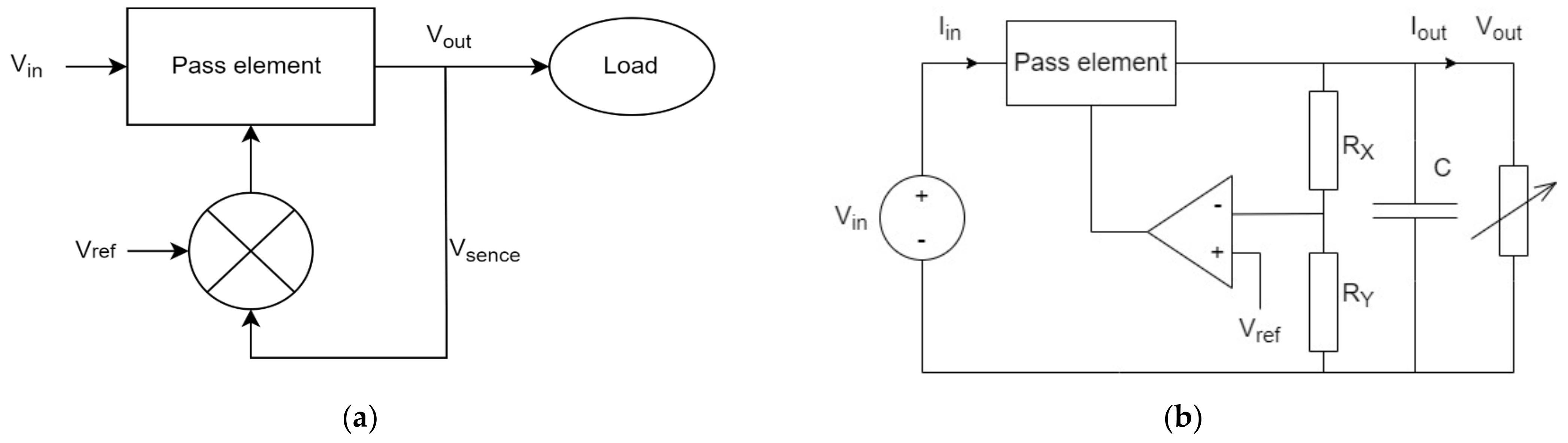
The basic concept of a linear regulator is to use a series pass element to act as a variable resistor against the input voltage fluctuations and load current changes to supply a regulated output voltage [10]. Transistors or a combination of transistors are used as the series pass element and using a feedback control loop, as shown in Figure 4a. The voltage drop across the series pass element is controlled to regulate the output voltage via the reference voltage (Vref).
As shown in Figure 4b, a voltage comparator is used to generate the feedback signal, and a simple voltage divider circuit is used as the feedback. With the assumption of ideal op-amps, output voltage can be formulated as in Equation (3) [11].
The efficiency of the linear regulator () approximately can be calculated by Equation (4) [11] as follows:
where is the current used by the control circuit, which is usually referred to as ground pin current. The efficiency of the linear regulator can therefore be improved by designing a control circuit with minimum ground pin current. In addition, it is important to note that efficiency is when the ground pin current is negligibly small.
Compared with the SMPS, there are specific advantages of using linear regulators such as low cost, low noise, and design simplicity, and the major advantage of using linear regulators is the excellent transient response to load current fluctuations [3]. However, linear regulators can only be used in applications where the input and the output voltage difference is very small. Otherwise, the efficiency is compromised. Low-dropout regulators (LDOs) are introduced to overcome the efficiency issues associated with linear regulators.
The name LDO is denoted because of the small voltage difference in dropout () between the input () and the output () voltages (see Equation (5) [11]).
Power consumption across the LDO () can be formulated as in Equation (6).
where is the quiescent current. When the dropout voltage is high, the power dissipated through the LDO is high. The first term of Equation (6) represents the power dissipated through the series pass element. Therefore, LDOs are typically used in applications where the dropout voltage is very small. In addition, the lower the dropout voltage, the higher the efficiency is. The second part of Equation (6) represents the power consumed by the controlling circuits. Most commercially available LDOs have a very small ground pin current. As a result, the power consumed by the control circuit is very low, and this improves the efficiency of the LDO.
An LDO uses a single transistor as the series pass element. PMOS and the NMOS are the two widely used CMOS devices and, of the two, NMOS have the lowest ON resistance. However, when using an NMOS device as the pass element, the charge pump is required to drive the NMOS, which makes the design complex and requires more PCB area. Due to the aforementioned disadvantages of NMOS, generally, PMOS is used as the pass element of the LDOs. Further details are given by Gunawardane [12].
4. Dominant Characteristics of LDOs
LDOs currently available in the market have quite a number of unique advantages when used in portable devices, as noted in the subsections below.
4.1. Higher Efficiency
The efficiency of an LDO is highly dependent on the dropout voltage. There are ultra-low-dropout regulators which achieve a high level of efficiency. Table 2 shows some commercially available highly efficient ultra-low-dropout regulators. The LDOs used for this comparison are selected based on those specifications suitable for portable device power supplies.
4.2. Low Noise
LDOs are capable of filtering noise and ripples while operating as voltage regulators due to their high-power supply rejection ratio (PSRR). Therefore, LDOs can generate a clean DC voltage without noise components, which prevents the resetting of sensitive devices and minimises distortions in signals due to noise. Usually, standard LDOs have an integral noise above 50 uVRMS. In addition, there are specific low-noise LDOs where the noise level is less than 30 uVRMS, such as TPS7A8101 [18], TPS74401 [19], and TPS7H1210-SEP [20].
4.3. Low Quiescent Current
4.4. Better Transient Performances
LDOs can overcome transient fluctuations without needing any additional components. Regardless of the sudden variations in the input side, LDOs are capable of keeping the output voltage stable. There are specially designed LDOs for fast input variation applications, such as TPS57140-Q1 [22], where the slew rate is 1.2 V/µs, and the better transient performance is a very important factor when supplying power for microprocessors.
4.5. Small Package Size
Compared with SMPS, where external components such as inductors need to be connected, LDOs are normally available as a single integrated component which makes them a perfect solution for portable devices.
Table 3 shows some of the LDO ICs in the market specifically designed for particular applications based on their dominant LDO characteristic.
5. Current LDO Application Trends and Their Market Share
Due to the excessive nature of communication and signal processing happening inside industrial automation systems, it is mandatory for them to have a noise-free clean power supply, as well as to maintain very low EMI levels [33]. EMI issues can cause serious errors in sensor measurements and PLC processing [34]. Because of their very low EMI levels and the ability to filter the noise components, LDOs have become popular in industrial automation systems [33]. Furthermore, with the simple compact design of LDOs such as ADP166 [26], TPS720 [24], and TLV733P [25], LDOs are the perfect alternative to the SMPS.
Today’s technology trend is to use more artificial intelligence and machine learning concepts in portable devices such as mobile phones, laptops, tablets, etc. In addition, in the modern world, most consumer devices tend to be portable/wireless. This concept involves a higher level of signal processing requirement. According to Moore’s law, the number of transistors on a microchip doubles every two years, but the cost of computers is halved [35]. This statement clearly indicates that usage of microprocessors and microcontrollers will be further increased in future electronic devices. Figure 6 [36] shows the growth prediction for transistors until 2030.
For portable devices, battery life and compactness are the major criteria of design. With these requirements, there is a challenge to design highly efficient power supplies with very low levels of noise, no EMI issues, and better transient performance. Due to their unique properties, as described in the above sections, LDOs are widely used in industry and consumer devices. As shown in Figure 7 [37], due to the high demand for consumer devices, the LDOs market is quickly growing. The price of the LDO is also comparatively cheap, which is another reason why the market for LDOs is growing. Major LDO producers are consistently trying to introduce more enhanced versions of LDOs to keep up with the competition. As an example, in 2019, Texas Instruments introduced an ultra-low-dropout regulator (TPS7A02 [38]) which has the smallest quiescent current of 25 nA in the industry [38].
6. LDO’s Recent Research Trends
With the growing market for LDOs, researchers are focused on further expanding the horizons of currently available LDOs. With the high level of LDO applications in portable devices, major LDO manufacturers and researchers are keen to further enhance the performance of LDOs [39]. The efficiency of LDOs, size of LDOs, and the noise and EMI levels of LDOs are the major key areas of high concern for enhanced performance of portable devices.
6.1. Improving the Compactness
An output capacitor that connects to the LDO is very useful in an intrinsic manner for reduced noise level, smoothing voltage spikes, handling fast load current variations, and improving the PSRR [40]. The dominant pole of LDO is simply created by a gigantic off-chip capacitor placed at the output of the LDO [41]. Normally, output capacitors are bulky, and due to the requirement of output capacitor, the LDO chip needs to accommodate additional pins so that the pin count increases. However, with state-of-the-art chip designs, bulky output capacitors compromise the compactness aspects of the design. Therefore, researchers are currently investigating designing capacitorless LDOs [42,43]. The challenge is to develop a capacitorless LDO without compromising the positive effects of the output capacitor in the LDO [44]. Li et al. [44] propose a push–pull buffer for driving the pass transistor in the LDO. As an example, Texas Instruments TPS744xx series is capable of stable operation using much smaller ceramic capacitors [19].
6.2. Reducing Noise Levels Further
The requirement for noise-free power supplies is increasing due to the rapidly increasing use of microcontrollers and processors in portable electronic devices. Increasing the PSRR is a commonly used approach to address this issue [45]. The higher the PSRR, the lower the ripples in output voltage [45]. PSRR is higher when the dropout voltage (voltage across the drain and the source of PMOS) is higher because when the voltage across the drain and the source of PMOS is high, the operating point is within the saturation region where the PMOS series resistance is lowest. When the dropout voltage is low, the operating point of PMOS moves to the triode region, where PMOS resistance is higher than the PMOS on resistance in the saturation region. With lower resistance, a higher level of noise will pass from the input to the output of LDO [46]. Therefore, there is a trade-off between the PSRR and the efficiency of LDOs [47]. Researchers are focused on developing synchronous digital LDOs to overcome this issue [48,49]. A digital error amplifier is in the synchronous digital LDO, and an external sampling clock is used in the feedback controller and the comparator [50].
6.3. Improving the Transient Performance
Transient responses have unique features that inherently connect to the application. Therefore, by considering the special properties of the application, LDOs can further be improved to withstand transients. Researchers are now focusing on developing LDOs for specific applications while considering the transient behaviours of the application [51]. Huang et al. [51] reviewed the benefits of using analog and digital LDOs based on the environment and also discussed the advantages of using hybrid LDOs such as analog-assisted digital LDOs and digital-assisted analog LDOs.
There are LDOs especially developed for flash memory systems [52]. A fully integrated digitally assisted LDO was proposed for NAND flash systems using a 500 nm I/O CMOS transistor. The proposed LDO’s input voltage range is 2.3–3 V and output is 2.1 V and it is capable of achieving both fast transient response and highly accurate regulation in the steady state. The measured output voltage drop is 225 mV against a load current step fluctuation of 150 mA in 20 ns.
Huang et al. [53] proposed a nano-ampere LDO to be used in IoT devices considering their exact transient properties. As shown in Figure 8a,b, the proposed setup consists of two LDO setups where the input is 1 V and the output is 0.8 V. Figure 8a shows the LDO 1 which combines dynamic current biasing techniques to reduce the quiescent current, while Figure 8b shows the LDO 2 consisting of an inverter-based dynamic loop to further improve the transient response. This prototype was fabricated in a 65 nm low-leakage CMOS process and tested against a transient fluctuation of a load current stepped from 100 nA to 10 mA in 1 µs transition time. The measured output voltage undershoot for LDO 1 is 336.8 mV, and 196 mV for LDO2.
6.4. Improving the Efficiency
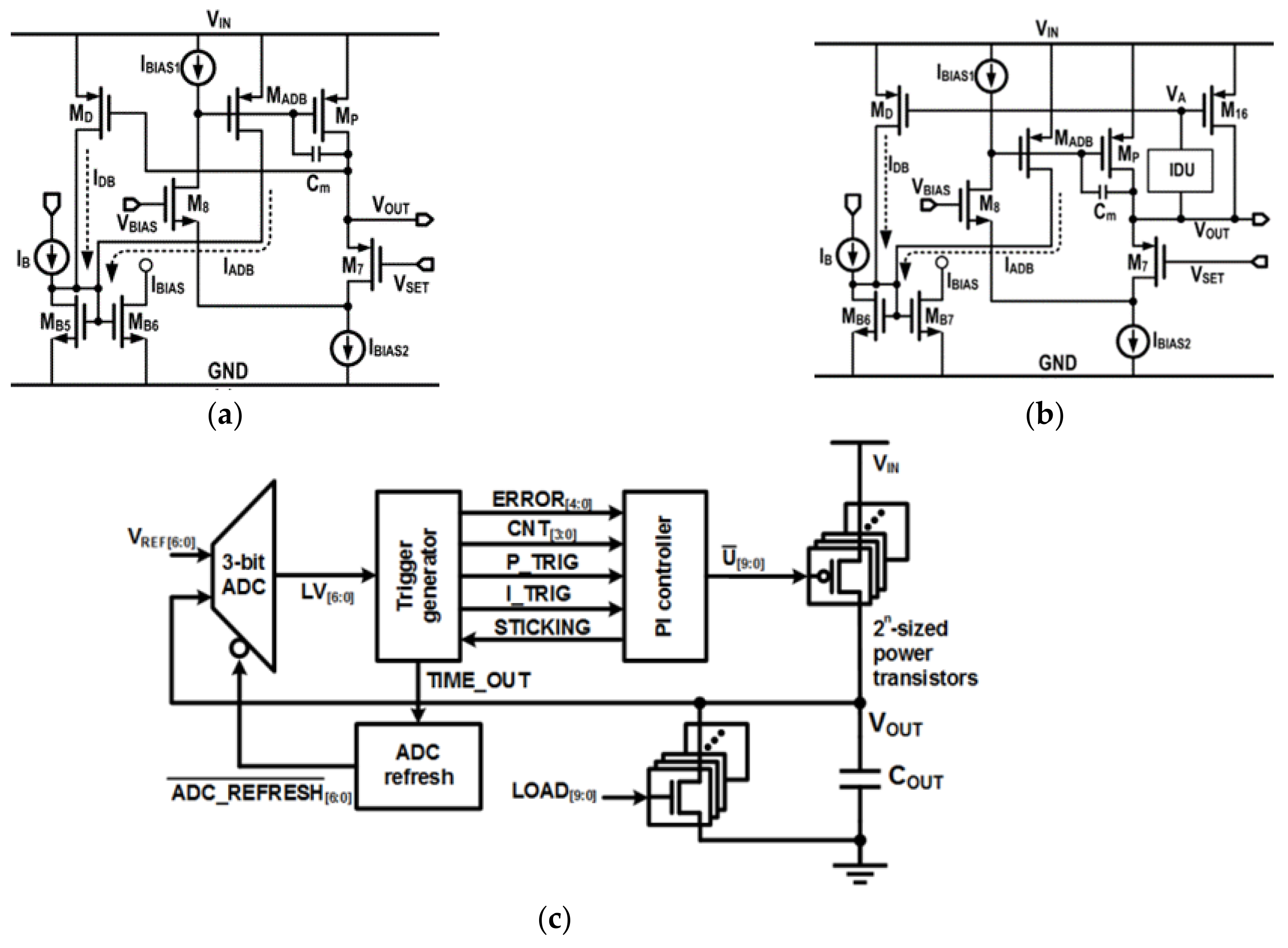
Many researchers focus on designing control circuits for LDOs with minimum power consumption. Control circuits consist of high-frequency processors that continuously monitor the regulated voltage of the LDO and generate feedback according to the regulated voltage. Currently, researchers are focused on using approaches such as time-coding architectures [54] to drive LDO control circuits. Time-driven controllers operate at every clock edge. If the LDO output varies after a locking edge, the controller captures the deviation at its next cycle. As shown in Figure 8c [54], the authors proposed an architecture consisting of analog-to-digital converter with a refresh circuit, proportional–integral controller, and a power transistor. By using time-coding architectures, LDO control circuits can be operated as event-driven controllers instead of continuously operating. As a result, consumption of quiescent current has been significantly reduced and the efficiency has increased to 93.6% [54].
7. Current Context of Portable Power Supply Designs
The power supply design is considered an integral part of the overall system design of a portable device due to important design constraints determined by the user requirements, such as longer battery life and reduced power consumption.
The most common storage technology that is used in today’s power supplies is the Li-ion battery [55]. Driven by the volume of the portable device market, the Li-ion batteries provide the best combination of power density and cost. The typical operating range of Li-ion batteries is 3.0 V to 4.2 V, which is a very convenient voltage because fewer cells are required in many applications [56]. Li-ion batteries have a high energy density and also the self-discharge rate of Li-ion batteries is very low; typically 5% in the first 4 h and dropping down to around 1 to 2% per month [57]. In addition, Li-ion batteries have a higher number of lifetime charge–discharge cycles and they do not require regular maintenance, unlike other available batteries that require regular discharge to overcome the memory effect [58]. There is no requirement for priming Li-ion batteries as there is for nickel-based rechargeable batteries. Apart from these advantages, there are two major drawbacks of Li-ion batteries, which are poor robustness and flammability [59]. As a result, a high degree of protection is required against overcharge and excessive discharge.
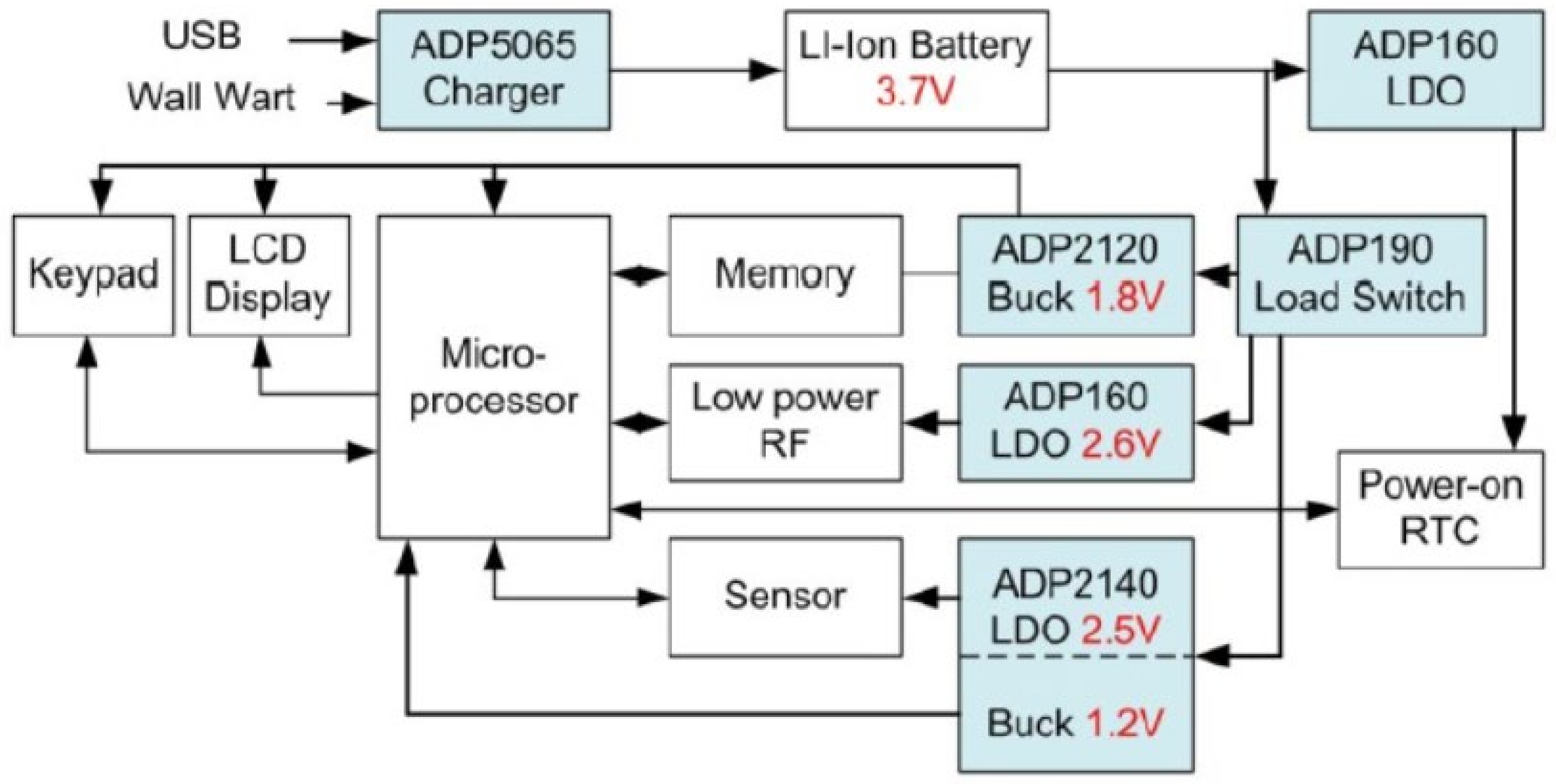
Portable devices normally have a combination of subsystems that require different voltage levels. As shown in Figure 9 [60], modern portable devices such as mobile phones, tablets, and portable electronic medical devices consist of many subsystems: batteries, memory, display, peripherals, etc. [60]. Those components operate at various voltage levels based on their requirements. When designing powering techniques for these subsystems, it is very important to verify that it produces the desired voltage level regardless of the following:
- Variation of the current consumed by the subsystem.
- Fluctuation of the battery voltage in the portable device.
- Variations due to operating conditions of the device, such as temperature.
Power supply requirements for a given application depend on many factors, and we can divide these into two different areas, namely, (I) primary specifications and (II) secondary specifications. Primary specifications include:
- Output rail voltage.
- Maximum load current.
- Output impedance of the power supply.
- Noise and ripple allowed.
- Input voltage range.
- Efficiency.
- Weight/volume of the power supply.
Secondary specifications include:
- Transient response capability and transient response.
- Radio frequency interference/electromagnetic interference (RFI/EMI).
- Reliability and the age of the power supply.
Usually, for very large power requirements for a given output voltage and maximum current requirement, end-to end-efficiency (ETEE) is a critical factor, and this value depends on the design of the power supply. SMPSs are theoretically 100% efficient, based on the assumption that switches, inductors, and capacitors used are ideal. However, six secondary losses associated with a DC–DC converter reduce the ETEE to a lower value, and these six main losses are summarised in Table 4.
In a linear regulator, Items 2 and 3 are nonexistent, and Item 1 is mainly dependent on the input to output voltage difference. LDO achieves higher efficiency by maintaining the input to output voltage difference at a very small value, usually in the range of a few tens of millivolts to fractional volts, giving a high ETEE of approximately of Vout/Vin.
When a small volume or weight is a primary target for a DC–DC converter, the switch-mode approach pushes the designer to move into higher frequencies, and this, in turn, increases the contribution by Items 2, 3, and 4. However, in an LDO, Items 2 and 3 are completely nonexistent, while capacitor losses are only related to the ripple of the power supply.
A switch-mode power supply brings the additional major issue of RFI/EMI, which requires added circuitry of filters at the input and output side of a DC–DC converter in general. The non-ideal nature of capacitors and inductors used in the circuit for this filtering contributes additionally to Items 2 and 3 in general.
When the secondary requirements of a converter are dictated by the load, sometimes a pure switch-mode converter does not satisfy the case. A classic example of this is in mobile phones and other portable devices where a large amount of mixed-signal circuitry is used. In these situations, the most useful secondary properties, such as Items 1 and 2 in an LDO or a linear converter, are used by cascading the output of the switch-mode converter with the input of an LDO for the overall achievement of the wider specifications of the power management system.
In summary, a switch-mode converter is utilized when the primary specifications are critically important. However, when the load side cannot tolerate limitations such as Items 1 to 3 above, a low component count LDO is used or an LDO is placed in tandem with a switch-mode converter. A more detailed discussion on this is available in [3].
Therefore, inside each portable device, there is a requirement for multiple voltage levels, and DC–DC voltage converters are used to convert voltages to the various levels. Based on the application’s requirements, the best technology is selected for portable devices. Efficiency, noise levels, EMI levels, and the compactness of the converter are some commonly considered factors when selecting a voltage converter for a portable device [61].
With the noise-sensitive nature of the portable devices due to communication requirements, LDO regulators are used as post-regulators in portable devices, which provides a sustainable market share for the linear regulator manufacturers [62].
8. Future Prospects for LDO Regulators in Power Supplies
It is evident that LDO has become an essential component in portable device design. However, the efficiency of the LDO is inversely proportional to the voltage difference between the input and the output. Consequently, the input and output voltage differences of LDOs need to be kept very small to achieve higher efficiencies [63]. Modern portable devices consist of multiple subsystems which require different operating voltages. These subsystems in portable devices are powered using a technique called point of load (POL), where multiple regulators stages are used [64]. It is difficult to power POL using SMPS due to their high noise, slow slew rate, and the complex nature of their output impedance [65]. With the presence of high-frequency switching in SMPS, noise and EMI levels can be increased [3]. LDOs are coupled to the output stage of SMPS as post regulators to satisfy the power requirements of the subsystems in portable devices [66]. Nonetheless, it becomes a costly and complex power management solution. However, when LDOs are coupled with SMPS, there are some technical challenges, such as the additional space requirement and the LDO’s output current limitations due to temperature rise. To address these technical challenges, Linear Technologies introduced a solution combining a high-efficiency SMPS with multiple LDOs in a single package (LTM8001 [67]), as shown in Figure 10a,b, [68] and Figure 10a [68] shows a single 2.5 V, 5 A regulator from a 12 V supply. In Figure 10a [68], LDO 1 to LDO 5 are connected in parallel with SMPS to produce a 2.5 V, 5 A output. In the configuration of Figure 10a [68], SMPS in LTM8001 produces an output of 3 V and each LDO has a dropout voltage of 500 mV where LDOs operate at their rated load current condition of 1.1 A.
Figure 10b [68] shows a dual output regulator which can generate outputs of 5 V and 3.3 V from a 12 V supply. In the configuration of Figure 10b [68], SMPS in LTM8001 produces an output of 5.5 V. LDO 1 and LDO 2 are connected in parallel to produce the 5 V output. Since LDO 1 and LDO 2 have 500 mV dropout voltages, they can operate at their rated load current condition of 1.1 A. Therefore, the 5 V output has the capability of delivering 2 A. LDOs from 3 to 5 are used to produce a 3.3 V output. Due to the high dropout voltage, each LDO’s output current degrades to 330 mA and, as a result, the 3.3 V output can only deliver an output current of 1 A.
The combined LDO and SMPS technique still needs further development to enhance the higher current capabilities and to reduce noise levels, but compared with the LDOs and SMPS, the SMPS + LDO technique is comparatively complex.
9. Supercapacitor-Assisted Low-Dropout Regulators (SCALDO) as a Solution to the Linear Regulator Efficiency Problem
When the dropout voltage becomes higher, linear regulators have very low efficiency due to power loss across the series pass element. As a solution to this issue of low efficiency in linear regulators, the concept of the lossless voltage dropper approach is used in the SCALDO technique.
9.1. Supercapacitors as Lossless Voltage Droppers
The SCALDO technique works on the simple principle that an ideal capacitor provides a voltage drop across its terminals, with the option to reuse that stored energy later. However, a small-value capacitor, such as an electrolytic of the order of microfarads, will fully charge in a short time if placed in series with an LDO and will block the current path.
Within the past two decades, supercapacitors (SCs) with capacitance values from 1 to 100,000 F in a single cell have entered the market [69]. With the same canister size as electrolytic and film capacitors, SCs offer at least a million times bigger capacitance while their ESR is in the range of 0.1 mΩ to 100 mΩ. [60]. With the capacitance in the order of farads, when they are placed in series with a resistive load such as a loaded LDO, they create charging circuits with a very long time constant, allowing the designer to use very slow speed switches for transferring the energy back to the LDO with ease. Commercial supercapacitor families today come in four different sub-categories, namely, (i) symmetrical supercapacitors, (ii) hybrid supercapacitors, (iii) battery capacitors, and (iv) Li supercapacitors. More details are given by Gunawardane [12]. Out of these types, symmetrical SCs come in values varying from 0.1 F to over 3000 F, and their ESR values vary from 100 mΩ to 0.1 mΩ, respectively [54]. Table 5 provides a generalised range of specifications for symmetrical-type SCs, available in the commercial market [69,70,71].
Typically, supercapacitors having a capacitance of 50 F or less have an ESR value between 20 mΩ and 100 mΩ [54]. If we compare these values with the MOSFETS used inside an LDO IC, they are comparable to, or lower than, the ON resistance of the MOSFET, and hence useful in connecting in series with an LDO as a lossless dropper.
9.2. Concept of SCALDO
When a precharged large capacitor is placed in series with the input path of an LDO, it keeps on accumulating the series drop, reducing the voltage drop across the series pass transistor of the LDO, assuming that the input DC voltage is constant.
The voltage change (dv) of a capacitor with time is given by Equation (7) [72] as follows:
where is the capacitance and is the instantaneous current through the capacitor. For a constant load current, if the capacitance is very large, will be very small over time, and it takes a long time to block the DC path.
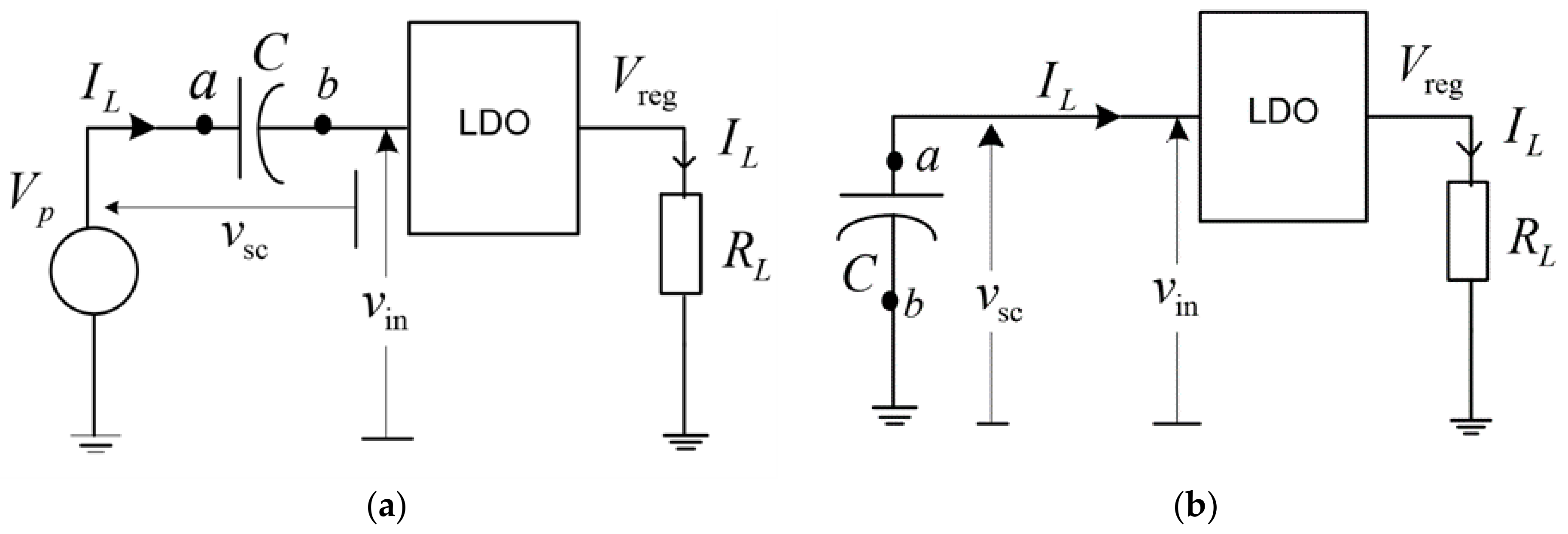
Figure 11a depicts how this simple series connection helps in improving the efficiency of an LDO. If the capacitor CSC has an initial voltage of , input voltage at the input of LDO () will be expressed as Equation (8),
As it carries on charging, at a later moment, the LDO will reach its minimum value for the correct operation of the LDO and at that point, the SC will have to be placed in parallel with the input of the LDO, as shown in Figure 11b. During this time, the input voltage source is disconnected, and the SC discharges back to LDO, to maintain the charge balance of the SC.
When considering the current flow during phases 1 and 2, the charge balance of the supercapacitor following connection can be formulated as in Equation (9) [72].
where , , and are the charging, discharging times, and current consumed by the load, respectively. By simplifying Equations (9) and (10), it can be formulated as follows.
With the above connection in Equation (10), the average current drawn from the unregulated power supply can be formulated as in Equation (11) [72],
Assuming there is no current drawn for the control circuit, the efficiency of the SCALDO can be derived as in Equation (12) [72],
From Equation (12), it can be seen that the efficiency of a SCALDO is two times higher than the typical regulator. As shown in Figure 12a [5], an experimental setup of 12 V to 5 V SCALDO was implemented to verify the proposed SCALDO technique. The 12 V to 5 V SCALDO was implemented using MCP1827 LDO from Microchip. As shown in Figure 12c, the maximum theoretical efficiency of a conventional 12–5 V LDO lies between 38–43% [73]. The 12–5 V SCALDO prototype achieved an overall end-to-end efficiency of 70–83.3% [73]. The setup was tested against a load current between 100–800 mA and the switching frequency is between 0.05 to 4 Hz, which is a very low operating frequency compared to SMPS.
Instead of using a single supercapacitor depending on the requirements, an array of SCs can be used as a voltage dropper element. This further-extended concept is discussed in [74]. Using the SCALDO technique, LDOs can operate with a higher level of difference between input–output voltages without compromising efficiency. The integrated circuit version of SCALDO has been designed as in Figure 12b and is currently in the testing phase.
9.3. Advantages of Using SCALDO in Portable Devices
For portable applications, SCALDO technique has much greater advantages compared to the currently used switch mode + LDO combination, mainly because the SCALDO prototype IC (Figure 12b) design provides a huge reduction of PCB space without the bulky inductors required in the case of SMPS. Another prominent characteristic of SCALDO is very low EMI and noise level, which is due to the very-low-frequency operation in the range of Hz to MHz. This will be used to a good advantage in portable devices that commonly consist of microcontrollers and processors. This will eliminate the need for additional filters.
9.4. Limitations of SCALDO Technology
Even though SCALDO technology has many salient advantages, there are a few areas with limitations; primarily minor effects due to the component constraints. The efficiency in SCALDO design is constrained by the ESR and the leakage current losses in the supercapacitors. As mentioned above, ESR values of supercapacitors are in the range of 0.1 mΩ to 100 mΩ [69] and the leakage current of supercapacitors is in the range of 5 to 50 µA [77]. Generally, both ESR and the leakage current of supercapacitors have very small values and the losses due to ESR and the leakage current can be negligible.
The control circuitry power consumption is the other factor. In an integrated design, this can be minimised to a significantly small value with the right component selection.
10. Conclusions
Linear regulators are no longer obsolete; instead, they have a dominant market in portable devices with the introduction of LDOs. LDOs come in the form of ICs, typically outputting up to about 5 A load current, and they are low in cost compared to the switch-mode stages within a PMS. LDOs have excellent EMI characteristics as well as low noise output and high current slew rates. With these desirable features, there is a dominant position for LDOs in portable device power supplies to be supplemented at post regulator stage to overcome major issues in SMPS.
Many researchers are currently working to improve the performance of LDOs in terms of efficiency, noise levels, compactness, and transient characteristics. Currently, the efficiencies of LDOs in the market are in the range of 96.25 to 98.55%, which are comparable to SMPS efficiencies. In larger systems, where larger currents are required, a discrete transistor-based LDO implementation is possible, provided the designer keeps the dropout voltage at a very low value to achieve high efficiency.
A newer extra-low-frequency SCALDO design approach summarised in this article demonstrates a unique way to achieve quasi-linear DC–DC converters where a high-efficiency LDO can be combined with a supercapacitor front end for loss recovery, creating a high-end-to-end-efficiency converter.
Author Contributions
Conceptualisation, K.G.; methodology, N.P.; formal analysis, N.P., K.G., N.K. and K.S.; investigation, N.P., K.G. and K.S.; writing—original draft preparation, N.P. and K.G.; writing—review and editing, N.P., K.G., K.S., N.K. and T.T.L., visualisation, N.P.; supervision, K.G. and N.K. All authors have read and agreed to the published version of the manuscript.
Funding
This research was funded by Advanced Energy Technology Project (AETP) grant from the Ministry of Business Innovation and Enterprise (MBIE), New Zealand, to develop the Future Architecture Network (FAN), grant number [UOCX2007] And The APC was funded by FAN project grant too.
Institutional Review Board Statement
Not applicable.
Informed Consent Statement
Not applicable.
Data Availability Statement
Not applicable.
Acknowledgments
We would like to acknowledge the support for our work from the researchers of Future Architecture Network (FAN) project.
Conflicts of Interest
The authors declare no conflict of interest.
Nomenclature
| SMPS | Switch-mode power supplies |
| SCC | Switched capacitor converters |
| PMS | Power management system |
| ESR | Equivalent series resistance |
| LDO | Low-dropout regulator |
| ETEE | End-to-end efficiency |
| POL | Point of load |
| SCALDO | Supercapacitor-assisted LDO |
| EMI | Electromagnetic interference |
| PSRR | Power supply rejection ratio |
| SC | Supercapacitor |
| Vref | Desired voltage in volts |
| Vout | Output voltage in volts |
| Iq | Current used by the control circuit in amps |
| Vin | Input voltage in volts |
| Vd | Dropout voltage in V |
| PD | Power consumption across LDO in watt |
| C | Capacitance in farads |
| dv | Voltage change |
| i(t) | Instantaneous current through the capacitor in amps |
| tcharging | Charging time in seconds |
| tdischarging | Discharging time in seconds |
| IAVG | Average current drawn from the unregulated power supply in amps |
References
- Darwish, M. Role of Semiconductor Devices in Portable Electronics Power Management. In IEE Colloquium on Recent Advances in Power Devices (Ref. No. 1999/104); IET: London, UK, 1999; pp. 1–4. [Google Scholar]
- Fernando, J. 5—Electrical Double-Layer Capacitors: Fundamentals, Characteristics, and Equivalent Circuits. In Energy Storage Devices for Electronic Systems; Kularatna, N., Ed.; Academic Press: Boston, MA, USA, 2015; pp. 149–186. ISBN 978-0-12-407947-2. [Google Scholar]
- Kularatna, N. DC Power Supplies: Power Management and Surge Protection for Power Electronic Systems; CRC Press: Boca Raton, FL, USA, 2018; ISBN 978-0-415-80248-2. [Google Scholar]
- Tuite, D. Inventor Updates a Classic 30 Years Later. 2007. Available online: https://www.electronicdesign.com/technologies/boards/article/21777220/inventor-updates-a-classic-30-years-later (accessed on 10 February 2022).
- Subasinghage, K.; Gunawardane, K.; Kularatna, N. Comparison of step-down charge pump converters and supercapacitor-assisted low- dropout (scaldo) regulators. In Proceedings of the TENCON 2021—2021 IEEE Region 10 Conference (TENCON), Auckland, New Zealand, 7–10 December 2021; pp. 299–304. [Google Scholar]
- Subasinghage, K.; Gunawardane, K.; Kularatna, N. Circuit Protection Techniques for Supercapacitor-Assisted Low-Dropout (SCALDO) Regulator. In Proceedings of the TENCON 2021—2021 IEEE Region 10 Conference (TENCON), Auckland, New Zealand, 7–10 December 2021; pp. 851–856. [Google Scholar]
- Xin, P.; Xue, J.; Mi, H. Research on Switch Power Supply Device. In Proceedings of the 2017 7th International Conference on Education, Management, Computer and Society (EMCS 2017), Shenyang, China, 17–19 March 2017. [Google Scholar]
- Mohan, N.; Undeland, T.M.; Robbins, W.P. Power Electronics: Converters, Applications, and Design; Wiley: Hoboken, NJ, USA, 1995; ISBN 978-0-471-58408-7. [Google Scholar]
- Femia, N.; Vitelli, M. Resistive losses of conductors carrying SMPS current waveforms. In Proceedings of the 2002 IEEE International Symposium on Industrial Electronics, L’Ayuila, Italy, 8–11 July 2002; Volume 9, pp. V-852–V-855. [Google Scholar]
- Rincon-Mora, G. Analog IC Design with Low-Dropout Regulators (LDOs), 1st ed.; McGraw-Hill, Inc.: New York, NY, USA, 2009; ISBN 978-0-07-160893-0. [Google Scholar]
- Zhang, H. Basic Concepts of Linear Regulator and Switching Mode Power Supplies 2013; Analog Devices: Norwood, MA, USA, 2013. [Google Scholar]
- Gunawardane, K. 6—Supercapacitor as a Lossless Dropper in DC-DC Converters. In Energy Storage Devices for Electronic Systems; Kularatna, N., Ed.; Academic Press: Boston, MA, USA, 2015; pp. 187–225. ISBN 978-0-12-407947-2. [Google Scholar]
- STMicroelectronics International N.V. 200 MA Very Low Quiescent Current Linear Regulator IC in (0.47 × 0.47) mm2 STSTAMPTM Package 2021; STMicroelectronics International N.V.: Geneva, Sitzerland, 2021. [Google Scholar]
- Texas Instruments. 1.5 A Low-Dropout Linear Regulator with Programmable Soft-Start 2020; Texas Instruments: Dallas, TX, USA, 2017. [Google Scholar]
- STMicroelectronics International N.V. 150 MA Low Quiescent Current and Low Noise Voltage Regulator, LD39015 2015; STMicroelectronics International N.V.: Geneva, Switzerland, 2015. [Google Scholar]
- Texas Instruments. TPS7A54 4-A, High-Accuracy (0.5%), Low-Noise (4.4 ΜVRMS), LDO Voltage Regulator 2020; Texas Instruments: Dallas, TX, USA, 2020. [Google Scholar]
- Texas Instruments. TLV752 Dual, 1-A, High-Accuracy, Adjustable-LDO in a Small-Size Package 2020; Texas Instruments: Dallas, TX, USA, 2020. [Google Scholar]
- Texas Instruments. TPS7A8101 Low-Noise, Wide-Bandwidth, High PSRR, Low-Dropout 1-A Linear Regulator 2015; Texas Instruments: Dallas, TX, USA, 2015. [Google Scholar]
- Texas Instruments. TPS74401 3.0-A, Ultra-LDO with Programmable Soft-Start 2017; Texas Instruments: Dallas, TX, USA, 2017. [Google Scholar]
- Nogawa, M. LDO Noise Examined in Detail 2012; Texas Instruments: Dallas, TX, USA, 2012. [Google Scholar]
- Low Quiescent Current (IQ) LDO Regulators—STMicroelectronics. Available online: https://www.st.com/en/power-management/low-iq-ldo-regulators.html (accessed on 6 February 2022).
- Texas Instruments. TPS57140-Q1 1.5-A 42-V Step-Down DC-DC Converter with Eco-ModeTM Control 2016; Texas Instruments: Dallas, TX, USA, 2016. [Google Scholar]
- Texas Instruments. Low-Noise, High-Bandwidth PSRR, Low-Dropout, 150-MA Linear Regulator 2006; Texas Instruments: Dallas, TX, USA, 2016. [Google Scholar]
- Texas Instruments. TPS720 350 MA, Ultra-Low VIN, RF Low-Dropout Linear Regulator With Bias Pin 2015; Texas Instruments: Dallas, TX, USA, 2015. [Google Scholar]
- Texas Instruments. TLV733P Capacitor-Free, 300-MA, Low-Dropout Regulator in 1-mm × 1-mm X2SON Package 2019; Texas Instruments: Dallas, TX, USA, 2019. [Google Scholar]
- Analog Devices. Ultralow Quiescent Current, 150 MA, CMOS Linear Regulators Data Sheet ADP160/ADP161/ADP162/ADP163 2013; Analog Devices: Norwood, MA, USA, 2013. [Google Scholar]
- Analog Devices. Ultralow Noise, 200 MA Linear Regulator Data Sheet ADM7160 2014; Analog Devices: Norwood, MA, USA, 2014. [Google Scholar]
- Texas Instruments. TPS7A19 40-V, 450-MA, Wide VIN, Low IQ, Low- Dropout Voltage Regulator with Power Good 2016; Texas Instruments: Dallas, TX, USA, 2016. [Google Scholar]
- Texas Instruments. TPS7B69xx-Q1 High-Voltage Ultra-Low IQ Low-Dropout Regulator 2015; Texas Instruments: Dallas, TX, USA, 2015. [Google Scholar]
- Analog Devices. 3µA IQ, 20mA Low Dropout Linear Regulators, LT3009 Series 2007; Analog Devices: Norwood, MA, USA, 2007. [Google Scholar]
- STLQ50—50 mA, 3 µA Supply Current Low Drop Linear Regulator—STMicroelectronics. Available online: https://www.st.com/en/power-management/stlq50.html (accessed on 7 February 2022).
- LDK715—High Input Voltage 85 MA LDO Linear Regulator—STMicroelectronics. Available online: https://www.st.com/en/power-management/ldk715.html (accessed on 7 February 2022).
- Gonzalez, J. Linear Power for Automated Industrial Systems; Texas Instruments: Dallas, TX, USA, 2017; p. 6. [Google Scholar]
- Zhang, Y.; Rasmussen, K. Detection of electromagnetic interference attacks on sensor systems. In Proceedings of the 2020 IEEE Symposium on Security and Privacy (SP), San Francisco, CA, USA, 18–21 May 2020; pp. 203–216. [Google Scholar]
- Holt, W. 1.1 Moore’s law: A path going forward. In Proceedings of the 2016 IEEE International Solid-State Circuits Conference (ISSCC), San Francisco, CA, USA, 31 January–4 February 2016. [Google Scholar] [CrossRef]
- Shalf, J. The Future of Computing beyond Moore’s Law. Philos. Trans. R. Soc. A Math. Phys. Eng. Sci. 2020, 378, 20190061. [Google Scholar] [CrossRef] [PubMed] [Green Version]
- Low Dropout (LDO) Linear Regulators Market Research: Global Status & Forecast by Geography, Type & Application (2015–2025). Available online: https://marketintellica.com (accessed on 7 February 2022).
- Texas Instruments. TPS7A02 Nanopower IQ, 25-NA, 200-MA, Low-Dropout Voltage Regulator With Fast Transient Response 2020; Texas Instruments: Dallas, TX, USA, 2020. [Google Scholar]
- Nogawa, M. A Topical Index of TI LDO Application Notes 2019; Texas Instruments: Dallas, TX, USA, 2019. [Google Scholar]
- Man, T.Y.; Leung, K.N.; Leung, C.Y.; Mok, P.K.T.; Chan, M. Development of Single-Transistor-Control LDO Based on Flipped Voltage Follower for SoC. IEEE Trans. Circuits Syst. I Regul. Pap. 2008, 55, 1392–1401. [Google Scholar] [CrossRef] [Green Version]
- Ho, M.; Guo, J.; Mak, K.H.; Goh, W.L.; Bu, S.; Zheng, Y.; Tang, X.; Leung, K.N. A CMOS Low-Dropout Regulator With Dominant-Pole Substitution. IEEE Trans. Power Electron. 2016, 31, 6362–6371. [Google Scholar] [CrossRef]
- Ahmed, F.U.; Sandhie, Z.T.; Chowdhury, M.H. An implementation of external capacitor-less low-dropout voltage regulator in 45 nm technology with output voltage ranging from 0.4 V–1.2 V. In Proceedings of the 2020 IEEE 38th International Conference on Computer Design (ICCD), Hartford, CT, USA, 18–21 October 2020; pp. 453–456. [Google Scholar]
- Liu, X.; Zhan, C.; Qiao, H. Chip-area-efficient capacitor-less LDO regulator with fast-transient response. In Proceedings of the 2019 IEEE International Conference on Integrated Circuits, Technologies and Applications (ICTA), Chengdu, China, 13–15 November 2019; pp. 27–28. [Google Scholar]
- Li, Q.; Wang, K.; Zhao, J. A Capacitor-less LDO with fast transient response using push-pull buffer. In Proceedings of the 2019 IEEE International Conference on Electron Devices and Solid-State Circuits (EDSSC), Xi’an, China, 12–14 June 2019; pp. 1–3. [Google Scholar]
- Ho, M.; Leung, K.N.; Or, P.Y.; Guo, J. Analysis of CMOS low-dropout regulator—Power-supply rejection ratio. In Proceedings of the 2014 IEEE Asia Pacific Conference on Circuits and Systems (APCCAS), Ishigaki, Japan, 17–20 November 2014; pp. 109–112. [Google Scholar]
- Park, J.-E.; Hwang, J.; Oh, J.; Jeong, D.-K. 32.4 A 0.4-to-1.2 V 0.0057 mm2 55 fs-transient-FoM ring-amplifier-based low-dropout regulator with replica-based PSR enhancement. In Proceedings of the 2020 IEEE International Solid-State Circuits Conference (ISSCC), San Francisco, CA, USA, 16–20 February 2020; pp. 492–494. [Google Scholar]
- Akram, M.A.; Hwang, I.-C.; Ha, S. Architectural Advancement of Digital Low-Dropout Regulators. IEEE Access 2020, 8, 137838–137855. [Google Scholar] [CrossRef]
- Ooishi, T.; Komiya, Y.; Hamade, K.; Asakura, M.; Yasuda, K.; Furutani, K.; Kato, T.; Hidaka, H.; Ozaki, H. A Mixed-Mode Voltage down Converter with Impedance Adjustment Circuitry for Low-Voltage High-Frequency Memories. IEEE J. Solid-State Circuits 1996, 31, 575–585. [Google Scholar] [CrossRef]
- Hazucha, P.; Moon, S.T.; Schrom, G.; Paillet, F.; Gardner, D.; Rajapandian, S.; Karnik, T. High Voltage Tolerant Linear Regulator With Fast Digital Control for Biasing of Integrated DC-DC Converters. IEEE J. Solid-State Circuits 2007, 42, 66–73. [Google Scholar] [CrossRef]
- Okuma, Y.; Ishida, K.; Ryu, Y.; Zhang, X.; Chen, P.-H.; Watanabe, K.; Takamiya, M.; Sakurai, T. 0.5-V input digital LDO with 98.7% current efficiency and 2.7-ΜA quiescent current in 65 nm CMOS. In Proceedings of the IEEE Custom Integrated Circuits Conference 2010, San Jose, CA, USA, 19–22 September 2010; pp. 1–4. [Google Scholar]
- Huang, M.; Lu, Y.; Martins, R.P. Review of Analog-Assisted-Digital and Digital-Assisted-Analog Low Dropout Regulators. IEEE Trans. Circuits Syst. II Express Briefs 2021, 68, 24–29. [Google Scholar] [CrossRef]
- Yoon, K.-S.; Kim, H.-S.; Qu, W.; Yuk, Y.-S.; Cho, G.-H. Fully Integrated Digitally Assisted Low-Dropout Regulator for a NAND Flash Memory System. IEEE Trans. Power Electron. 2018, 33, 388–406. [Google Scholar] [CrossRef]
- Huang, Y.; Lu, Y.; Maloberti, F.; Martins, R.P. Nano-Ampere Low-Dropout Regulator Designs for IoT Devices. IEEE Trans. Circuits Syst. I: Regul. Pap. 2018, 65, 4017–4026. [Google Scholar] [CrossRef]
- Kim, D.; Seok, M. A Fully Integrated Digital Low-Dropout Regulator Based on Event-Driven Explicit Time-Coding Architecture. IEEE J. Solid-State Circuits 2017, 52, 3071–3080. [Google Scholar] [CrossRef]
- Cericola, D.; Novák, P.; Wokaun, A.; Kötz, R. Hybridization of Electrochemical Capacitors and Rechargeable Batteries: An Experimental Analysis of the Different Possible Approaches Utilizing Activated Carbon, Li4Ti5O12 and LiMn2O4. J. Power Sources 2011, 196, 10305–10313. [Google Scholar] [CrossRef]
- Israelsohn, J. Battery Management Included. EDN. 2001. Available online: https://www.edn.com/battery-management-included/ (accessed on 12 February 2022).
- Juzkow, M.W.; St. Louis, C. Designing Lithium-Ion Batteries into Today’s Portable Products. In Proceedings of the Portable by Design Conference, Santa Clara, CA, USA, 25–28 February 1996; pp. 13–22. [Google Scholar]
- Lopez, J.; Gonzalez, M.; Viera, J.C.; Blanco, C. Fast-charge in lithium-ion batteries for portable applications. In Proceedings of the INTELEC 2004 26th Annual International Telecommunications Energy Conference, Chicago, IL, USA, 19–23 September 2004; pp. 19–24. [Google Scholar]
- Dileepan, V.M.; Jayakumar, J. Performance analysis of lithium batteries. In Proceedings of the 2017 International Conference on Innovations in Electrical, Electronics, Instrumentation and Media Technology (ICEEIMT), Coimbatore, India, 3–4 February 2017; pp. 330–333. [Google Scholar]
- Dostal, F. Power Management for Healthcare Applications|Analog Devices. Available online: https://www.analog.com/ru/technical-articles/power-management-for-health-care-applications.html (accessed on 6 February 2022).
- Saggini, S. Power management in battery powered handheld portable applications. In Proceedings of the 2015 Mobile Systems Technologies Workshop (MST), Milan, Italy, 22 May 2015; pp. 12–14. [Google Scholar]
- Manninger, M. Power management for portable devices. In Proceedings of the ESSCIRC 2007—33rd European Solid-State Circuits Conference, Munich, Germany, 11–13 September 2007; pp. 167–173. [Google Scholar]
- Kankanamge, K.; Kularatna, N.; Steyn-Ross, A. Laplace transform-based theoretical foundations and experimental validation—low frequency supercapacitor circulation technique for efficiency improvements in linear regulators. In Proceedings of the IECON 2011—37th Annual Conference of the IEEE Industrial Electronics Society, Melbourne, VC, Australia, 7–10 November 2011; pp. 4113–4118. [Google Scholar]
- Kankanamge, K.; Kularatna, N. Improving the end-to-end efficiency of DC–DC converters based on a supercapacitor-assisted low-dropout regulator technique. IEEE Trans. Ind. Electron. 2014, 61, 223–230. [Google Scholar] [CrossRef]
- Shen, Z.-H.; Min, H. Combination Method of DC-DC Converter and LDO to Improve Efficiency and Load Regulation. Electron. Lett. 2011, 47, 615–617. [Google Scholar] [CrossRef]
- Day, M. Integration Saves Time and Board Space Converter. Available online: https://www.electronicdesign.com/content/article/21186830/integration-saves-time-and-board-space (accessed on 8 February 2022).
- Analog Devices. LTM8001: 36 VIN, 5 A ΜModule Regulator with 5-Output Configurable LDO Array 2013; Analog Devices: Norwood, MA, USA, 2013. [Google Scholar]
- Andy, R. µModule Regulator Combines a Switcher with Five 1.1 A LDOs: Use Them for Multiple Low Noise Rails, or Parallel Them to Spread Heat and Share Current to 5 A; Analog Devices: Norwood, MA, USA, 2014. [Google Scholar]
- Samwha Capacitor Co., Ltd. ESD-SCAP; Samwha Capacitor Co., Ltd.: Gangnam, Korea, 2018. [Google Scholar]
- Kularatna, N.; Jayananda, D. Supercapacitor-Based Long Time-Constant Circuits: A Unique Design Opportunity for New Power Electronic Circuit Topologies. IEEE Ind. Electron. Mag. 2020, 14, 40–56. [Google Scholar] [CrossRef]
- Şahin, M.E.; Blaabjerg, F.; Sangwongwanich, A. A Comprehensive Review on Supercapacitor Applications and Developments. Energies 2022, 15, 674. [Google Scholar] [CrossRef]
- Gunawardane, K. Analysis on Supercapacitor Assisted Low Dropout Regulators. Ph.D. Thesis, University of Waikato, Hamilton, New Zealand, 2014. [Google Scholar]
- Kularatna, N.; Subasinghage, K.; Gunawardane, K.; Jayananda, D.; Ariyarathna, T. Supercapacitor-Assisted Techniques and Supercapacitor-Assisted Loss Management Concept: New Design Approaches to Change the Roadmap of Power Conversion Systems. Electronics 2021, 10, 1697. [Google Scholar] [CrossRef]
- Gunawardane, K.; Kularatna, N. Supercapacitor assisted ldo (scaldo) techniquean extra low frequency design approach to high efficiency DC-DC converters and how it compares with the classical switched capacitor converters. In Proceedings of the 2013 Twenty-Eighth Annual IEEE Applied Power Electronics Conference and Exposition (APEC), Long Beach, CA, USA, 17–21 March 2013; p. 1984, ISBN 978-1-4673-4354-1. [Google Scholar]
- Wickramasinghe, T. Supercapacitor-Based Linear Converter for Voltage Regulator Modules. Ph.D. Thesis, University of Waikato, Hamilton, New Zealand, 2016. [Google Scholar]
- Subasinghage, K.; Gunawardane, K.; Lie, T.T.; Kularatna, N. Single-input, dual polarity, dual output DC-DC converter implementation based on the SCALDO technique. In Proceedings of the 2017 IEEE International Conference on Industrial Technology (ICIT), Toronto, ON, Canada, 22–25 March 2017; pp. 207–212. [Google Scholar]
- Gunawardane, K.; Kularatna, N. Supercapacitor-assisted low dropout regulator technique: A new design approach to achieve high-efficiency linear DC–DC converters. IET Power Electron. 2018, 11, 229–238. [Google Scholar] [CrossRef]
Figure 1.
Block diagram of a generic power management system [1].
Figure 1.
Block diagram of a generic power management system [1].

Figure 2.
Evolution of power supply design technology.

Figure 3.
Efficiency vs. switching frequency variation in switching devices.

Figure 4.
(a) Linear regulator functional diagram; (b) basic linear regulator configuration.

Figure 5.
Basic quiescent current of typical LDOs [21].
Figure 5.
Basic quiescent current of typical LDOs [21].

Figure 6.
Semiconductor devices production [36].
Figure 6.
Semiconductor devices production [36].

Figure 7.
LDO market share [37].
Figure 7.
LDO market share [37].

Figure 8.
(a) Proposed structure of LDO 1 [53]; (b) proposed structure of LDO 2 [53]; and (c) LDO architecture with the proposed event-driven PI control systems [54]. Copyright 2022 IEEE.

Figure 9.
Subsystems of a portable device [60].
Figure 9.
Subsystems of a portable device [60].


Figure 11.
SCALDO configuration: (a) phase 1: supercapacitor charging circuit [72]; (b) phase 2: supercapacitor discharging circuit [72].

Figure 12.
(a) SCALDO 12 V–5 V discrete prototype [5]; (b) SCALDO IC; (c) comparison of end-to-end efficiency of the 12–5 V SCALDO [73].


Table 1.
Comparison of performance of SMPS, charge pumps, and linear regulators.
| Parameter | Linear Regulators and LDOs | SMPS | Charge Pumps |
|---|---|---|---|
| Design flexibility | Step down | Step up/Step down/Inversion | Step up/Step down/Inversion |
| Circuit Diagram |  LDO |  Buck Converter |  Switch capacitor voltage doubler |
| Efficiency (typical) | Linear regulators: 50–60% LDOs up to 98% | Higher than 95% | 70–80% |
| Complexity | Low | High | Low |
| Size | small | Smaller than LDO | Smallest |
| Total Cost | Low | High | Low |
| Electromagnetic interference (EMI) | Low | High | Medium |
| Noise | Low | High | Medium |
| Input voltage range | Narrow | Wide | Narrow |
| Thermal management | Moderate (mainly the series pass device) | Complex (multiple devices to deal with where the heat is dissipated) | Moderate (switches) |
| Output current capability | Medium | High | Low |
Table 2.
Commercial ultra-low-dropout regulators.
| Dropout Voltage (mV) | Input Voltage Range (V) | Output Voltage Range (V) | Current Rating (mA) | Maximum Efficiency (%) | Commercially Available LDOs |
|---|---|---|---|---|---|
| 200 | 1.5–5.5 | −0.3 ± 0.3 | 200 | 96.36 | LDBL20 [13] |
| 65–125 | 0.8–5.5 | 0.8–3.6 | 1500 | 97.72 | LD59150 [14] |
| 80 | 1.5–5.5 | 0.8–3.3 | 100 | 98.55 | LD39015 [15] |
| 175 | 1.1–6.5 | 0.8–5.15 | 4000 | 97.31 | TPS7A54 [16] |
| 225 | 1.5–6 | 0.55–5.5 | 1000 | 96.25 | TLV752 [17] |
Table 3.
Commercially available LDOs for specific applications.
| LDO Specific Property | Industrial Application | Commercially Available LDOs |
|---|---|---|
| Reduce noise and PSRR levels | High-speed communications applications, video processing applications, and high-accuracy measurement applications. | TPS717xx family [23] |
| Compactness | Compact portable devices | TPS720 [24], TLV733P [25], ADP160 [26], ADP166 [26], ADM7160 [27] |
| Lower quiescent current | Battery-powered applications | TPS7A19 [28], TPS7B69 [29], LT3009 [30], STLQ50 [31], LDK715 [32] |
Table 4.
Secondary losses of DC–DC converters.
| Item | Loss | Reason | Remarks |
|---|---|---|---|
| 1 | Static losses of the switches such as transistors and diodes |
| These show up a cumulative content known as “static losses” which increases with output voltage and the load current. |
| 2 | Dynamic losses in transistors and diodes increase with the switching frequency |
| The higher switching frequency of switch-mode power supplies increases the dynamic losses linearly with the frequency in general. |
| 3 | Secondary losses in inductors |
| Except for ohmic losses, others are frequency-dependent and have a nonlinear behaviour with frequency. |
| 4 | Secondary losses in capacitors |
| Smaller capacitors have high ESR and large capacitors have relatively lower ESR. |
| 5 | Power consumed by the controller circuit associated with the power stage |
| These losses depend on the control circuit section of the switch-mode power supply. |
| 6 | PCB track losses/interconnection losses in an IC version |
| The larger the current the higher these are. |
Table 5.
Supercapacitor specifications.
| Parameter | Unit | Range |
|---|---|---|
| Rated voltage | V | 1.2–3.8 |
| Capacitance | F | 1–3000 |
| Specific energy density | Wh/kg. | 1–10 |
| Specific power density | W/kg | <10,000 |
| Cycle life | Cycle number | >50,000 |
| Charge and discharge efficiency | % | 85–98 |
| Fast charge duration | Seconds | 0.3–30 |
| Fast discharge duration | Seconds | 0.3–30 |
| Shelf life | Years | 20 |
| Operating temperature | °C | −40 to 75 |
Publisher’s Note: MDPI stays neutral with regard to jurisdictional claims in published maps and institutional affiliations. |
© 2022 by the authors. Licensee MDPI, Basel, Switzerland. This article is an open access article distributed under the terms and conditions of the Creative Commons Attribution (CC BY) license (https://creativecommons.org/licenses/by/4.0/).
Share and Cite
MDPI and ACS Style
Gunawardane, K.; Padmawansa, N.; Kularatna, N.; Subasinghage, K.; Lie, T.T. Current Context and Research Trends in Linear DC–DC Converters. Appl. Sci. 2022, 12, 4594. https://doi.org/10.3390/app12094594
AMA Style
Gunawardane K, Padmawansa N, Kularatna N, Subasinghage K, Lie TT. Current Context and Research Trends in Linear DC–DC Converters. Applied Sciences. 2022; 12(9):4594. https://doi.org/10.3390/app12094594
Chicago/Turabian StyleGunawardane, Kosala, Nisitha Padmawansa, Nihal Kularatna, Kasun Subasinghage, and Tek Tjing Lie. 2022. "Current Context and Research Trends in Linear DC–DC Converters" Applied Sciences 12, no. 9: 4594. https://doi.org/10.3390/app12094594
Note that from the first issue of 2016, this journal uses article numbers instead of page numbers. See further details here.