Routes to increase performance for antimony selenide solar cells using inorganic hole transport layers
 Stephen Campbell1
  Laurie J. Phillips2
  Jonathan D. Major2
  Oliver S. Hutter1 Ryan Voyce1
  Yongtao Qu1* Neil S. Beattie1 Guillaume Zoppi1
  Vincent Barrioz1*
- 1Department of Mathematics, Physics and Electrical Engineering, Northumbria University, Newcastle Upon Tyne, United Kingdom
- 2Department of Physics, University of Liverpool, Liverpool, United Kingdom
Simple compound antimony selenide (Sb2Se3) is a promising emergent light absorber for photovoltaic applications benefiting from its outstanding photoelectric properties. Antimony selenide thin film solar cells however, are limited by low open circuit voltage due to carrier recombination at the metallic back contact interface. In this work, solar cell capacitance simulator (SCAPS) is used to interpret the effect of hole transport layers (HTL), i.e., transition metal oxides NiO and MoOx thin films on Sb2Se3 device characteristics. This reveals the critical role of NiO and MoOx in altering the energy band alignment and increasing device performance by the introduction of a high energy barrier to electrons at the rear absorber/metal interface. Close-space sublimation (CSS) and thermal evaporation (TE) techniques are applied to deposit Sb2Se3 layers in both substrate and superstrate thin film solar cells with NiO and MoOx HTLs incorporated into the device structure. The effect of the HTLs on Sb2Se3 crystallinity and solar cell performance is comprehensively studied. In superstrate device configuration, CSS-based Sb2Se3 solar cells with NiO HTL showed average improvements in open circuit voltage, short circuit current density and power conversion efficiency of 12%, 41%, and 42%, respectively, over the standard devices. Similarly, using a NiO HTL in TE-based Sb2Se3 devices improved open circuit voltage, short circuit current density and power conversion efficiency by 39%, 68%, and 92%, respectively.
1 Introduction
Antimony selenide (Sb2Se3), as a simple and low-cost compound with a direct energy band gap (∼1.18 eV), high absorption coefficient (
A number of studies have reported that Sb2Se3 thin films with preferred crystallographic orientation along the (hk1) direction, particularly (221), resulted in devices with higher efficiencies (Leng et al., 2014; Yuan et al., 2016; Li et al., 2017). The improved performance is often attributed to increased charge transport through the (hk1)-oriented ribbons perpendicular to the substrate and benign grain boundaries in this material (Chen et al., 2017; Williams et al., 2020). Wang and co-workers demonstrated the dependence of Sb2Se3 PV device performance on the preferred crystal orientation of the absorber (Wang et al., 2017). In that work, by optimising growth conditions, Sb2Se3 solar cells with preferred (211) and (221)-orientations on CdS and ZnO achieved higher efficiencies (5.6% and 6.0%, respectively) than those with (020) and (120)-orientations (3.2% and 4.8%, respectively). For planar Sb2Se3 solar cells in substrate orientation, a record efficiency of 6.5% has been reported with the Cd0.75Zn0.25S buffer layer being used as an alternative to CdS (Figure 1A shows standard substrate device). Meanwhile, Sb2Se3 devices with this buffer layer but in a superstrate structure (Figure 1B) have achieved an efficiency of 7.6% (Wen et al., 2018). Recently, a record substrate device efficiency of 9.2% was obtained by growing (001)-oriented Sb2Se3 nanorod arrays on sputtered molybdenum layers (Li et al., 2019). A conformal interfacial TiO2 layer was used to mitigate the migration of elemental antimony (Sb) into the CdS buffer layer, as interdiffusion has been shown to create a detrimental CdSe interlayer (Phillips et al., 2019).
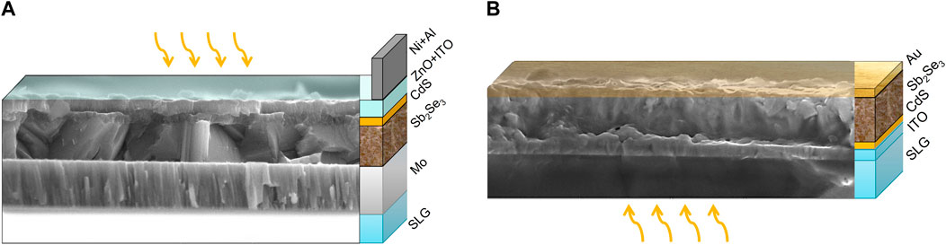
FIGURE 1. Standard planar (A) substrate and (B) superstrate configuration Sb2Se3 solar cells.
In this work, thin transition metal oxides, NiO and MoOx, are applied as HTLs in substrate Sb2Se3 devices to improve carrier selectivity at the back electrode by controlling inter-diffusion and formation of secondary phase materials (such as MoSe2) at the interface. Additionally, NiO and MoOx HTLs are deposited on superstrate Sb2Se3 films before making Au back contacts to alter the energy band alignments at the back contact effectively producing an electron reflector, and minimising carrier recombination.
In the first part of this study, Sb2Se3 substrate/superstrate device simulations using solar cell capacitance simulator (SCAPS) are conducted in order to interpret the effect of HTLs on Sb2Se3 device characteristics (Burgelman et al., 2000). We then characterise the material properties of MoOx and NiO thin films deposited at room temperature by electron beam evaporation. At this temperature it was found that NiO formed a crystalline film, unlike MoOx which was amorphous. Sb2Se3 absorber films were then fabricated by close-space sublimation (CSS) and thermal evaporation (TE) techniques and incorporated into superstrate and substrate solar cell configurations. HTLs were inserted at the metal electrode/Sb2Se3 absorber interface and their effect on Sb2Se3 crystallinity and solar cell performance is comprehensively studied.
2 Experimental section
2.1 Device fabrication
The basic structure of substrate Sb2Se3 solar cells was as follows: Soda lime glass (SLG)/Mo/Sb2Se3/CdS/ZnO/ITO/Ni-Al. Mo coated soda lime glass (SLG) substrates measuring 7.5 cm2 × 2.5 cm2 were used in this study. NiO or MoOx HTLs were deposited between the Mo electrode and Sb2Se3. Thin HTL films of 15 nm thickness were deposited using e-beam evaporation. 500 nm thick Sb2Se3 layers were prepared by TE of crystalline/powder Sb2Se3 source material (Alfa Aesar, 99.99%) at a deposition rate of ∼15 Å/s. The substrates were maintained at a temperature of 300°C throughout the deposition. The Sb2Se3 films were subsequently subjected to a heat treatment at 300°C for 30 min in Ar atmosphere in a tube furnace to promote recrystallisation. For the CSS Sb2Se3 films, a compact seed layer was grown at 0.05 mbar N2 for 5 min with a source temperature of 350°C, followed by a 30 min growth step at 13 mbar and a source temperature of 450°C to produce a compact and highly orientated grain structure. The substrate was then rapidly cooled with N2. An n-type CdS buffer layer (∼60 nm) was deposited by chemical bath deposition followed by DC-pulsed sputtering deposition of an i-ZnO (∼35 nm) layer plus a transparent conductive window layer ITO (∼200 nm). Front contact grids comprising Ni (∼50 nm) and Al (∼1,000 nm) were deposited through a shadow mask by e-beam evaporation. Finally, 0.16 cm2 cells were defined by mechanical scribing on each substrate.
Superstrate Sb2Se3 solar cells have the following configuration: SLG/ITO/CdS/Sb2Se3/Au with NiO or MoOx HTLs deposited between the metal contact and Sb2Se3 absorber. The ITO layer was deposited by DC-pulsed sputtering and Sb2Se3 layers were grown by TE and CSS as detailed above. Finally, Au back contacts with an area of 0.07 cm2 were deposited through a shadow mask by e-beam evaporation.
2.2 Material and device characterisation
The crystal structures of Sb2Se3 were characterised by X-ray diffraction (XRD) with Cu Kα1 (1.54056 Å) radiation (Rigaku SmartLab SE). The surface morphology and cross-sectional images of Sb2Se3 films were taken by scanning electron microscopy (SEM, Tescan Mira 3 FEG-SEM). Optical spectroscopy measurements were performed using a Shimadzu UV-2600 spectrophotometer fitted with an integrating sphere. Kelvin probe force microscopy (KFPM) measurements were done using a KP Technology KP020 single point kelvin probe system fitted with a standard 2 mm Au tip.
Current-density vs. voltage (J-V) measurements of Sb2Se3 thin film solar cells were performed using an Abet Technologies solar simulator at 1-sun (100 mW/cm2) illumination equivalent to air mass 1.5 global spectrum with light power density calibrated using a Si reference cell.
2.3 Device simulation
Device simulation was carried out for both substrate and superstrate configuration Sb2Se3 solar cell using Solar Cell Capacitance Simulator (SCAPS 1-D), which is based on the solutions to Poisson’s equation and continuity equation for electrons and holes in the vertical heterostructure of multilayer thin film PV device (Burgelman et al., 2000). The input parameters of the solar cells were defined with the Sb2Se3, HTL and electron transport layer (ETL) semiconducting properties, including experimentally determined bandgaps, electron affinity, density of states (Zeng et al., 2016), mobility of charge carriers (Chen et al., 2017), acceptor/donor concentrations (Wang et al., 2015), and defect state density (Leijtens et al., 2016). Defects were introduced at the Sb2Se3/CdS interface to simulate realistic device performance.
3 Results and discussion
3.1 Simulated Sb2Se3 devices
Simulation analysis using SCAPS software was implemented to evaluate the performance of reference substrate and superstrate Sb2Se3 solar cells and those incorporating MoOx and NiO as HTLs, subsequently referred to as samples Ref, MoOx and NiO, respectively (see Table 1 for film properties). Figure 2 shows the J-V curves and corresponding box plots of J-V parameters of both Sb2Se3 device configurations with incorporated HTLs. Regarding the substrate devices, all device parameters are improved, with the exception of Voc which shows a slight decrease for devices with a HTL (down from 0.423 V for the reference device to 0.408 and 0.411 V for MoOx and NiO devices, respectively). However, devices with MoOx HTL show evidence of roll-over behaviour. The roll-over phenomenon, which occurs near the Voc in a light J-V curve, is due to Schottky energy barrier formed at the absorber/metal interface at a solar cell back contact (Eisenbarth et al., 2011; Hädrich et al., 2011). It acts as a reverse biased diode when the main junction is forward biased, blocking carrier transport for increasing forward bias, resulting in roll-over behaviour in light J-V characteristics. The baseline Jsc in the reference device was 29.9 mA/cm2, rising to 31.2 and 31.3 mA/cm2 in MoOx and NiO devices, respectively. Addition of HTL films to the reference device demonstrated a notable increase in FF for substrate devices. The FF in the reference device was 47.0%, rising to a maximum of 55.6% and 56.0% in the MoOx and NiO devices, respectively. The increase in Jsc and FF of devices with integrated HTL materials directly translates into improvements in power conversion efficiency, PCE [η = 5.9% (Ref), 6.7% (MoOx) and 7.2% (NiO)]. The current-blocking energy barrier at the back contact of the MoOx substrate device could explain the lower PCE in comparison to the device with a NiO HTL. It is important to note that the results shown are not representative of the maximum conversion efficiencies that may be achieved with Sb2Se3, as we are focusing solely on the effect of the HTL, while using currently available materials parameters.
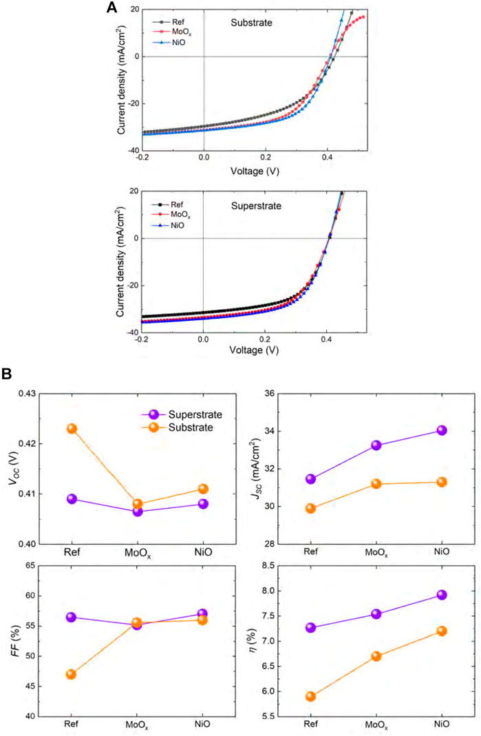
FIGURE 2. (A) J-V curves and (B) J-V parameters of simulated Sb2Se3 solar cells with different HTL materials. Roll-over behaviour is observed in the J-V curve of substrate devices with MoOx HTL.
For superstrate Sb2Se3 solar cells, devices with an incorporated HTL showed an increase in Jsc of around 8% from 31.5 mA/cm2 observed in the reference device to 33.5 and 34.0 mA/cm2 in the devices with a MoOx and NiO HTL, respectively. As a result of the improvement in Jsc, the PCE of solar cells with a HTL increased to 7.5% (MoOx) and 8.0% (NiO) from the reference value of 7.3%. Interestingly, no roll-over was seen in the J-V curve for the MoOx device which could be related to the use of Au as metallic back contact rather than Mo in the substrate devices. The work function (WF) of a metal employed as a rear contact on a PV device plays an important role in facilitating hole extraction at the contact (Fleck et al., 2020). Typically, Au is reported to have a WF of 5.10 eV (Michaelson, 1977) and Mo has WFs ranging from 4.50–4.95 eV, depending on the preferred crystal orientation of the metal (Green, 1969; Michaelson, 1977; Hölzl and Schulte, 1979). To illustrate the effect of back contact metal WF on substrate/superstrate Sb2Se3 device performance, Figure 3 shows the dependence of J-V parameters on the WF of Mo and Au metals. It is apparent that the J-V parameters of all substrate devices are sensitive to variations in the value of Mo WF. In the Ref and MoOx substrate devices, Voc decreases monotonically with Mo WF where a significant drop is observed from 0.432 V to 0.422 V at WF 4.95 eV to 0.036 V and 0.093 V at WF 4.50 eV for Ref and MoOx devices, respectively. This is a clear indication of an increasing back contact barrier with decreasing Mo WF. This phenomenon has been observed experimentally in Sb2Se3 solar cells previously (Liu et al., 2014; Li et al., 2017). The Voc in the NiO device is less affected by the Mo WF, reducing from 0.422 V at WF 4.95 eV to 0.319 V at WF 4.50 eV. A similar trend is seen in Jsc, FF and η parameters for the substrate devices. However, a low Mo WF of 4.50 eV causes a notable decrease in FF of the MoOx device (12.3%), compared to the Ref and NiO devices (26.0% and 32.4%).
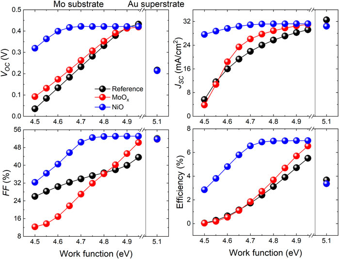
FIGURE 3. J-V parameters of simulated Sb2Se3 substrate devices with Mo back contact (varying Mo WF between 4.50–4.95 eV) and simulated Sb2Se3 superstrate devices with Au back contact (WF at 5.1 eV).
In order to understand the improvement of the device performance with the introduction of HTLs, it is necessary to consider the energy band alignment at the interfaces at the back of the PV devices. Figure 4 shows the simulated energy band diagrams of substrate and superstrate Sb2Se3 devices incorporating NiO and MoOx HTLs. Due to a small electron affinity (EA = 1.46 eV (NiO), 2.05 eV (MoOx)) and large band gaps (Eg ∼3.80 eV (NiO), 3.50 eV MoOxx)) in both HTL materials, a large potential energy barrier is formed at the back contact, reflecting electrons. This barrier minimises carrier recombination at the back interfaces with Sb2Se3 and improves conductivity at the back electrode. However, it is apparent that a non-negligible hole barrier of 0.26 and 0.29 eV is formed at the MoOx/Sb2Se3 interface of the substrate and superstrate devices, respectively, which can manifest as J-V roll-over behaviour seen in the simulated MoOx substrate device. Thus the SCAPS simulations indicate the incorporation of a MoOx or NiO HTL into substrate and superstrate configuration Sb2Se3 solar cells increases device performance compared to a standard solar cell by the introduction of a high energy barrier to electrons at the rear absorber/metal interface.
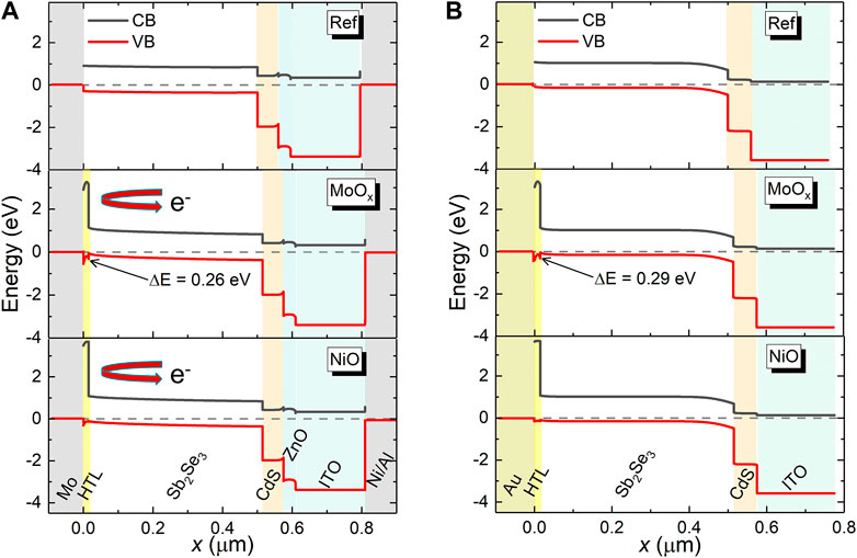
FIGURE 4. Energy level alignment for the devices in substrate (A) and superstrate (B) orientati1ons. Devices without a hole transport layer (top), with a MoOx layer (middle) and a NiO layer (bottom) are shown.
3.2 Fabricated Sb2Se3 devices
100 nm thick films of MoOx and NiO were deposited on SLG at room temperature to facilitate characterisation of the HTLs. Figure 5 shows surface morphology SEM images of the respective HTLs. The MoOx film exhibits an amorphous, flake-like structure in comparison to a compact crystalline morphology observed in the NiO film. XRD patterns in Figure 6 confirm the amorphous and crystalline nature of the MoOx and NiO films, respectively. All the diffraction peaks in the NiO thin film were identified and indexed to cubic NiO (JCPDS number 04-0835) and no diffraction peaks of other impurity phases were observed.
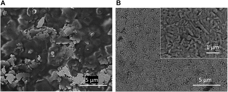
FIGURE 5. Top-down SEM image of a 100 nm (A) MoOx film and (B) NiO films on glass. Inset: Higher magnification image of the NiO film, showing the nanostructure.
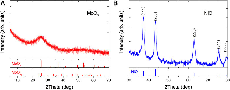
FIGURE 6. XRD pattern of 100 nm films of (A) MoOx and (B) NiO on soda lime glass (SLG). Reference XRD data for MoO2, MoO3 and NiO are shown underneath the XRD with JPDCS card ID 65-5787, 35-0609 and 04-0,835 respectively.
Supplementary Materials S1A shows the spectral transmittance and reflectance of the NiO and MoOx films on SLG. Both HTLs are highly transparent in the visible and near-infrared wavelength region and their transmittance falls sharply at ultraviolet wavelengths. However, the amorphous MoOx film has slightly lower transmittance/higher reflectance in the sub-600 nm wavelength region compared to the crystalline NiO film. The bandgap energy (Eg) of the HTL films was calculated by extrapolation of the linear region of the Tauc plot to the x-axis, according to the relation (Tauc et al., 1966):
where α is the absorption coefficient of the semiconductor material, h is Planck’s constant, ν is the frequency of the electromagnetic radiation and A is a constant of proportionality. The estimated Eg values of NiO and MoOx films are 3.95 and 3.85 eV, respectively (see Supplementary Materials S1B). A HTL film thickness of 15 nm was incorporated into the superstrate/substrate device to ensure a conformal coating of the HTL. A HTL requires a thickness sufficient to preserve the desired material properties and not impede charge transport considerably which would detrimentally increase series resistance in the finished devices.
3.3 Superstrate devices
TE and CSS deposition techniques were employed for Sb2Se3 film growth on SLG/ITO/CdS superstrates. For TE, the SLG/ITO/CdS superstrates were heated to 300°C prior to Sb2Se3 deposition in order to promote the growth of preferred (hk1) crystal orientations while minimising (hk0) orientations (Zhou et al., 2015) (hk0) planes, specifically (120), have been found to be detrimental to carrier transport (Guo et al., 2018; Wen et al., 2018; Li et al., 2019). The (hk0)-oriented Sb2Se3 nanoribbons are stacked parallel to the ITO/SLG superstrate where conductivity is inhibited by electrically insulating VdW bonds between the stacked nanoribbons. A seed layer is used in Sb2Se3 films deposited via CSS. This seed layer has a high density of nucleation points for the second stage of growth during the CSS process, which improves uniformity, raising the average efficiency of devices (Hutter et al., 2018a). Transmittance and reflectance data for a representative TE Sb2Se3 film was used to determine the Eg from a Tauc plot, which gave a Eg value of 1.17 eV in good agreement with (Birkett et al., 2018), see Supplementary Materials S2A,B. XRD patterns for Sb2Se3 films deposited by TE and CSS are shown in Figure 7A. The peaks in both XRD patterns are sharp and well resolved indicating the polycrystalline nature of the Sb2Se3 thin films. The lattice planes are cross-referenced to JCPDS card no. 15-0861 confirming the formation of orthorhombic Sb2Se3 with space group Pbnm. Both XRD patterns show similar characteristics, exhibiting strong (211) and (221) peaks with minimal contributions from (hk0) planes. Figures 7B–E shows the top and cross-sectional SEM images of Sb2Se3 thin films deposited by TE and CSS. The different growth techniques result in contrasting Sb2Se3 film morphologies. TE produces Sb2Se3 films of uniform thickness of ∼500 nm and densely packed grains, confirming the good crystallinity of the films, consistent with the XRD results (Figures 7B,D). However, this deposition method did not form a conformal coating of the Sb2Se3 film across the entire superstrate with the presence of pinholes observed, see Supplementary Materials S3A.
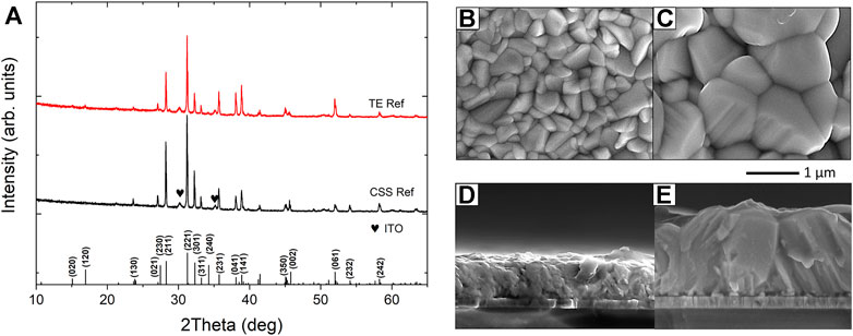
FIGURE 7. (A) XRD patterns of Sb2Se3 layers deposited by TE and CSS on ITO/CdS superstrates with standard diffraction pattern for Sb2Se3 (JCPDS15-0861) included for reference and SEM images of corresponding TE (B,D) and CSS (C,E) Sb2Se3 samples.
Conversely, CSS-grown Sb2Se3 films have a rough surface morphology with exceptionally large grains in comparison to the TE films and the grains extend the full depth of the layer. Larger grains are a prerequisite for better device performance as charge mobility is faster along the Sb2Se3 ribbons than hopping between the ribbons (see Figures 7C,E). The CSS films also showed a degree of porosity but not to the extent observed in the TE films, Supplementary Materials S3B. The presence of pinholes in the Sb2Se3 films is detrimental to device performance as shunting pathways may be formed upon subsequent deposition of the Au back contact (Hutter et al., 2018b).
J-V measurements under 1-sun illumination (100 mW/cm2) were performed on Sb2Se3 devices in the standard superstrate configuration and devices incorporating MoOx and NiO HTLs. The light J-V curves were fitted using a single diode model to extract the values of series (Rs) and shunt (Rsh) resistances. Figure 8 compares the statistical distribution of the key PV parameters for these devices, where a minimum of 10 cells of each device type were measured. On average, there was a slight increase in Voc when a NiO HTL was incorporated into the CSS device structure. Using a NiO HTL layer increased Voc to 0.226 V from values of 0.201 and 0.186 V for Ref and MoOx devices, respectively. The mean Jsc of NiO cells was also enhanced to 15.94 mA/cm2 compared to Ref (11.34 mA/cm2) and MoOx (10.54 mA/cm2) cells despite a slightly lower average FF in the NiO devices. This translates into a higher mean NiO CSS device efficiency of 1.01% with Ref and MoOx devices achieving efficiencies of 0.71 and 0.59% respectively. Notwithstanding the higher average Rs (2.6 Ωcm2) and lower Rsh (74 Ωcm2) values for NiO CSS solar cells compared to Ref (Rs = 2.9 Ωcm2, Rsh = 119 Ωcm2) and MoOx (Rs = 1.3 Ωcm2, Rsh = 167 Ωcm2) cells, using NiO as a HTL increases performance by boosting Jsc in CSS Sb2Se3 superstrate devices compared to the standard and MoOx based devices.
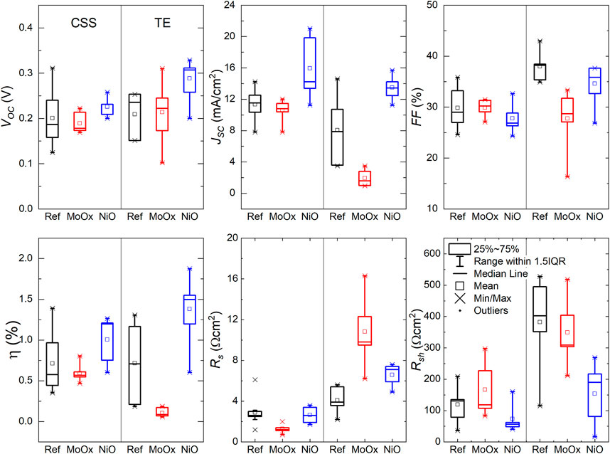
FIGURE 8. J-V parameters of superstrate TE and CSS Sb2Se3 devices with incorporated MoOx and NiO HTLs. □ is the average value and × is the minimum and maximum position. The three horizontal lines of each box stand for the 25%, 50%, and 75% of the reading distribution. The whisker range is determined by the standard deviation of the sampled devices. IQR is the inter-quartile range.
The average J-V parameters of TE Sb2Se3 superstrate devices followed a similar trend to those observed in the CSS devices [Voc: 0.209 V (Ref) → 0.214 V (MoOx) → 0.288 V (NiO), Jsc: 1.94 mA/cm2 (MoOx) → 8.05 mA/cm2 (Ref) → 13.48 mA/cm2 (NiO) ⇒ η: 0.10% (MoOx → 0.72% (Ref) → 1.38% (NiO)]. It is worth noting that the mean FF of the Ref TE cells (38.0%) was higher in relation to the cells with a HTL (27.2% MoOx, 34.6% NiO). This correlates to an increase in Rsh of 382 Ωcm2 in Ref samples from Rsh values of 349 Ωcm2 and 154 Ωcm2 measured in MoOx and NiO cells, respectively. In TE superstrate device configuration, the thin MoOx film appears to form a more resistive layer compared to Ref and NiO devices (Rs: 10.8 Ωcm2 MoOx, 4.1 Ωcm2 Ref and 6.6 Ωcm2 NiO). Thus, overall device performance in MoOx based solar cells is negatively impacted by low Jsc and high Rs which could be related to the amorphous nature of the MoOx thin film and the presence of a current-blocking barrier at the back contact highlighted in device simulations. Despite lower FF in NiO based solar cells, device efficiencies exceed those of Ref and MoOx TE devices due to improvements in Voc and Jsc showing the benefit of using NiO as a HTL in superstrate Sb2Se3 solar cells.
3.4 Substrate devices
Figure 9 shows the XRD patterns of substrate Sb2Se3 thin films deposited via TE and CSS. All diffraction peaks are in good agreement with the orthorhombic Sb2Se3 (JCPDS 15-0861), which presents in the form of (hk0), (hk1) or (hk2). No diffraction peaks of other impurity phases were observed. TE Sb2Se3 films on Mo and Mo/MoOx substrates show (020) and (120) peaks compared to all other Sb2Se3 films. The presence of (020) and (120) crystal orientations in thin Sb2Se3 films adversely affects PV device performance (Leng et al., 2014; Yuan et al., 2016; Li et al., 2017). However, when using a NiO HTL in TE Sb2Se3 films, it can be observed that the intensity of the diffraction peaks of Sb2Se3 is dominated by (221) and (211) crystal plane orientations. Furthermore, when using the Mo/NiO substrate, Sb2Se3 film shows an increased peak intensity for the (002) orientation. Since h and k miller indices have a zero value, it indicates that the (Sb4Se6)n ribbons grow perpendicular to the substrate surface (Li et al., 2019). For CSS Sb2Se3 films, Ref and MoOx samples demonstrate a higher (002) peak intensity than NiO.
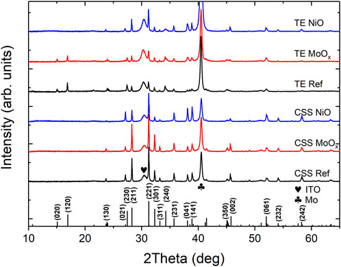
FIGURE 9. XRD patterns of Sb2Se3 films deposited by TE or CSS on top of NiO, MoOx and Mo-coated SLG.
Figures 10, 11 show SEM images of Sb2Se3 films on Mo-coated SLG deposited by TE and CSS methods, respectively. The top-down SEM images of the TE films (Figures 10A–C) show a difference in morphology depending on the presence of the underlying HTL. The MoOx sample exhibits larger Sb2Se3 grains than the Ref sample and the presence of pinholes in both samples is patently obvious. On the other hand, the Sb2Se3 grains in the NiO sample appear more angular in nature although pinholes are still present in the film. The dissimilarity in morphology is emphasised in SEM cross-section images of the TE Sb2Se3 films (Figures 10D–F). Voids at the absorber/Mo interface are apparent in the Ref TE sample whereas the MoOx sample shows a homogenous film with large grains. For the NiO sample, the Sb2Se3 grains appear column-like with no voids at the Mo interface. The top-down SEM image of all types of CSS Sb2Se3 thin films (Figures 11A–C) show significantly larger grains compared to the TE films. However, Sb2Se3 film in the Ref sample is on average thicker (∼1,000 nm) than the MoOx (∼550 nm) and NiO (∼700 nm), see Figures 11D–F. The NiO sample also has a smoother surface topography.
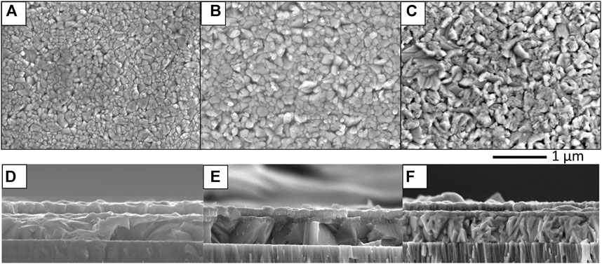
FIGURE 10. Top-down and cross-sectional SEM images of reference substrate (A,D), MoOx (B,E) and NiO (C,F) of Sb2Se3 films deposited by thermal evaporation.
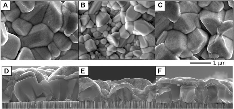
FIGURE 11. Top-down and cross-sectional SEM images of reference substrate (A,D), MoOx (B,E) and NiO (C,F) of Sb2Se3 films deposited by close-space sublimation.
To quantify the difference in orientations between the substrate Sb2Se3 thin films, the texture coefficient (TC) of diffraction peaks of the samples was calculated based on the following equation (Zoppi et al., 2006):
where I(hkl) is the measured peak intensity of (hkl) plane and I0 (hkl) the intensity in the standard XRD pattern. N is the total number of reflections considered for the calculation. A diffraction peak with a relatively large TC value (
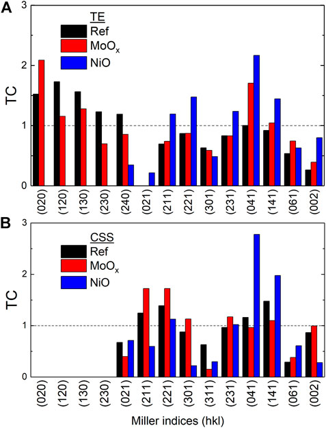
FIGURE 12. Texture coefficient analysis from XRD patterns of Sb2Se3 films deposited via TE (A) and CSS (B) with different hole transport layers in substrate configuration. A diffraction peak with a relatively large TC value (
Figure 13 shows the variation in J-V parameters measured for a minimum batch size of 10 Sb2Se3 solar cells in substrate configuration deposited by TE and CSS incorporating HTLs. The use of MoOx/NiO HTLs adversely affects all device parameters in CSS-based solar cells. This can be explained by lower average Rsh values of 55 Ωcm2 and 47 Ωcm2 determined for MoOx and NiO device types, respectively, compared to 172 Ωcm2 in the Ref devices. The reason for the reduction in Rsh of the substrate devices with a HTL is not obvious. Only working TE devices were achieved by incorporating a NiO HTL, which can be attributed to the templating effect of the NiO film which eliminated the deleterious (hk0) crystal planes and promoted the growth of preferred (211) and (221) planes. As highlighted in device simulations, the performance of substrate Sb2Se3 solar cells can be dependent on the WF of Mo back contact (see Figure 3). Mo metal typically has a WF in the range of 4.5–4.95 eV. KPFM measurements on Mo coated SLG prior to Sb2Se3 deposition determined the Mo WF to be 4.6 eV. According to simulations, device performance of Ref and MoOx substrate devices is severely impacted at the observed Mo WF. Simulated NiO device performance is affected to a lesser degree.
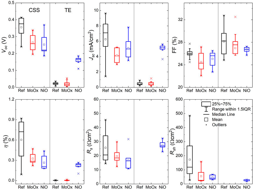
FIGURE 13. J-V parameters of substrate TE and CSS Sb2Se3 devices with incorporated MoOx and NiO HTLs. □ is the average value and × is the minimum and maximum position. The three horizontal lines of each box stand for the 25%, 50% and 75% of the reading distribution. The whisker range is determined by the standard deviation of the sampled devices. IQR is the inter-quartile range.
Rs values for both TE and CSS substrate Sb2Se3 devices were significantly higher than their superstrate counterparts and had a detrimental effect on overall substrate device performance. This could be related to a non-optimal sputtered ITO layer in the substrate devices with a typical sheet resistance of ∼ 35 Ω/□ (Qu et al., 2016) compared to commercially available ITO-coated glass slides used in superstrate devices with sheet resistances of 8–12 Ω/□ (Sigma Aldrich).
3.5 Simulated and fabricated device comparison
Experimentally determined device parameters, such as Rs and Rsh and apparent doping density (NA) of the Sb2Se3 absorber, were incorporated into SCAPS simulations of TE/CSS Sb2Se3 devices in superstrate/substrate configurations in order to replicate the observed behaviour of the fabricated devices. For an accurate representation of the fabricated cells, the NA value for the Sb2Se3 absorber in the CSS devices was set to a value previously determined for the same CSS deposition process used in this study with a Sb2Se3 absorber thickness of 1 μm (Phillips et al., 2019). An experimentally determined NA value for a typical 500 nm thick TE Sb2Se3 absorber was used in TE device simulations (see Table 1 for TE/CSS Sb2Se3 film properties). Figure 14 shows device performance of the simulated TE/CSS Sb2Se3 devices with experimentally determined Rs, Rsh and NA values. Similar trends are observed for all device parameters of the simulated and fabricated solar cells in both device configurations indicating the simulated devices are a reasonable representation of actual Sb2Se3 solar cells (see Figures 8, 13). However, in superstrate configuration, simulations overestimate all J-V parameters, indicating factors other than Rs, Rsh and NA are influencing device performance. Material properties such as carrier lifetimes, defects and band tails states have been cited as having a detrimental effect on overall device performance (Chen and Tang, 2020). In that work, a number of bulk defects in Sb2Se3 were identified with energy levels within the Sb2Se3 bandgap ranging from 0.18–0.94 eV above the valence band maximum. For simulation purposes, a mid-gap donor defect (0.62 eV) was introduced for the Sb2Se3 bulk to reproduce realistic device performance (Wen et al., 2018; Ma et al., 2020). Chen and Tang (2020) also highlighted significant recombination occurring at the n-p interface which severely impacts both Voc and Jsc. The presence of additional Sb2Se3 bulk defects and increased absorber/buffer interface defect concentration could account for the differences observed between the simulated and fabricated devices studied here.
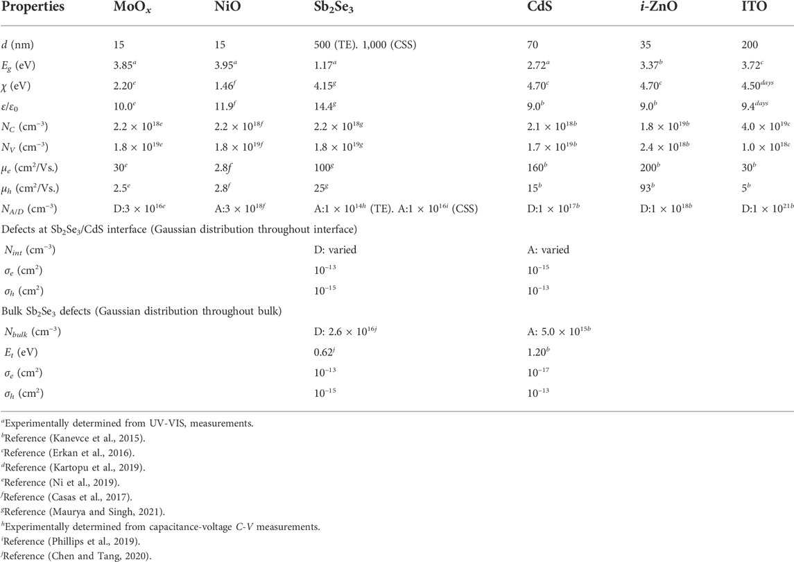
TABLE 1. Device simulation parameters, d: layer thickness, Eg: bandgap, χ: electron affinity, ɛ/ɛ0: dielectric constant, NC/V: effective density of states C: conduction band (CB) V: valence band (VB), μe,h: carrier mobility, NA/D: apparent doping density D: donor A: acceptor, σe,h: capture cross section, Nint: interface defect concentration, Et: defect energy level relative to CB/VB and Nbulk: bulk defect concentration. Subscripts e and h are electron and hole, respectively.
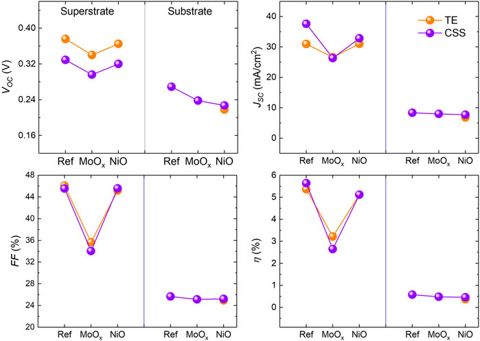
FIGURE 14. Comparison of J-V parameters of simulated TE and CSS Sb2Se3 solar cells with different HTL materials in substrate and superstrate device configurations.
In addition, it is worth noting actual superstrate devices which incorporate a MoOx HTL under-perform in relation to standard simulated superstrate devices (see Figure 8). This decrease in performance is not observed in the fabricated substrate Sb2Se3 solar cells with a MoOx HTL. This discrepancy can be accounted for by different processing conditions applied during deposition of substrate and superstrate devices. During deposition of Sb2Se3 layer on SLG/Mo/HTL substrate, the substrate temperature is maintained at 300°C which is sufficient to crystallise the MoOx film, see Supplementary Materials S4. The crystallised MoOx film consists of a mixture of MoO2, MoO3 and intermediate reduced oxide phases. The phase composition affects the electronic and optical properties of the MoOx film, with MoO2 content lowering the resistivity, transmittance and bandgap (Inzani et al., 2017). Simulations also show a roll-over in the J-V curves for superstrate Sb2Se3 devices in both configurations (see Figure 15), indicating the presence of a barrier to carrier transport at the back contact seen in simulated energy band alignments as previously discussed (Figure 4).
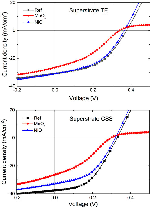
FIGURE 15. J-V curves for simulated TE and CSS Sb2Se3 devices with HTLs in superstrate configuration. Roll-over behaviour is evident in both TE and CSS devices with MoOx HTL indicating a carrier transport barrier at the back contact.
4 Conclusion
Numerical simulations of standard planar superstrate and substrate Sb2Se3 solar cells along with the effect of incorporating MoOx and NiO HTLs, demonstrated an increase in device efficiency for cells with a HTL which was achieved by an increase in Jsc for both substrate and superstrate device configurations. Both HTLs have high bandgaps and low electron affinities compared to Sb2Se3 absorber which manifests as a large barrier for electrons at the metallic back electrode and facilitates hole extraction. However, a roll-over effect was seen in the simulated J-V curve of the substrate device with MoOx HTL, suggesting a current-blocking barrier at the back contact caused by non-optimal energy band alignment. Material characterisation of the HTL materials deposited by E-beam evaporation at room temperature revealed MoOx formed an amorphous layer while NiO crystallised in cubic crystal orientation. 15 nm thick HTLs were incorporated into superstrate/substrate solar cells with Sb2Se3 absorbers deposited by thermal evaporation and close-space sublimation. For CSS superstrate solar cells with NiO HTL, device efficiency was enhanced by a 40% increase in Jsc compared to reference and MoOx based devices. TE superstrate cells incorporating NiO as HTL also demonstrated improved efficiencies achieved by higher Voc and Jsc. In the superstrate TE cells with MoOx HTL, Jsc was severely inhibited which is attributed to MoOx forming a more resistive layer due to its amorphous nature. Conversely, the presence of a MoOx or NiO HTL in substrate CSS-deposited Sb2Se3 solar cells reduced device performance which is linked to lower average Rsh observed in these cells. Optimisation of HTL thickness and/or re-optimisation of the absorber deposition could potentially alleviate this issue. Simulations reveal a connection between the WF of the Mo metal back contact and substrate device performance. For an experimentally determined Mo WF of 4.6 eV, all device J-V characteristics are significantly reduced, whereas substrate devices with NiO HTL are only marginally affected. In addition, XRD analysis of TE Sb2Se3 films with NiO HTL revealed a templating effect on Sb2Se3 crystal orientation where detrimental (020)/(120) crystal planes were eliminated and preferred (211)/(221) planes increased in intensity which resulted in increased device performance of substrate Sb2Se3 solar cells. NiO shows more promise as a HTL in Sb2Se3 PV devices, and crucially can act as a templating layer when the Sb2Se3 deposition method does not already impart the desired structure, as is often the case with TE devices.
Data availability statement
Data is available via this link: https://figshare.com/projects/Routes_to_Increase_Performance_for_Antimony_Selenide_Solar_Cells_using_Inorganic_Hole_Transport_Layers/140140.
Author contributions
SC, RV, LP, and JM fabricated absorbers and solar cells, SC conducted material and device characterisation, data analysis and device simulations. SC wrote the manuscript with contribution from OH. OH, YQ, VB, NB, and GZ discussed results and contributed to manuscript mofification and finalisation. VB and YQ supervised the project.
Acknowledgments
The authors acknowledge the EPSRC Centre for Doctoral Training in Renewable Energy Northeast Universities (ReNU) for funding through grant EP/S023836/1. The authors also appreciate the support from North East Centre for Energy Materials (NECEM) (EP/R021503/1) and British Council Newton Fund Institutional Links Grant in Ultralight Absorber for Remote Energy Source (U-AREs, No. 623804307). Discussions regarding NiO thin film deposition with Prof. Elizabeth Gibson, School of Natural and Environmental Sciences, Newcastle University is acknowledged.
Conflict of interest
The authors declare that the research was conducted in the absence of any commercial or financial relationships that could be construed as a potential conflict of interest.
Publisher’s note
All claims expressed in this article are solely those of the authors and do not necessarily represent those of their affiliated organizations, or those of the publisher, the editors and the reviewers. Any product that may be evaluated in this article, or claim that may be made by its manufacturer, is not guaranteed or endorsed by the publisher.
Supplementary material
The Supplementary Material for this article can be found online at: https://www.frontiersin.org/articles/10.3389/fchem.2022.954588/full#supplementary-material
References
Birkett, M., Linhart, W. M., Stoner, J., Phillips, L. J., Durose, K., Alaria, J., et al. (2018). Band gap temperature-dependence of close-space sublimation grown Sb2Se3 by photo-reflectance. Apl. Mater. 6, 084901. doi:10.1063/1.5027157
Black, J., Conwell, E., Seigle, L., and Spencer, C. (1957). Electrical and optical properties of some M2v−bN3vi−b semiconductors semiconductors. J. Phys. Chem. Solids 2, 240–251. doi:10.1016/0022-3697(57)90090-2
Burgelman, M., Nollet, P., and Degrave, S. (2000). Modelling polycrystalline semiconductor solar cells. Thin Solid Films 361-362, 527–532. doi:10.1016/S0040-6090(99)00825-1
Casas, G., Cappelletti, M., Cédola, A., Soucase, B. M., and Peltzer y Blancá, E. (2017). Analysis of the power conversion efficiency of perovskite solar cells with different materials as Hole-Transport Layer by numerical simulations. Superlattices Microstruct. 107, 136–143. doi:10.1016/j.spmi.2017.04.007
Chen, C., Bobela, D. C., Yang, Y., Lu, S., Zeng, K., Ge, C., et al. (2017). Characterization of basic physical properties of Sb2Se3 and its relevance for photovoltaics. Front. Optoelectron. 10, 18–30. doi:10.1007/s12200-017-0702-z
Chen, C., Li, W., Zhou, Y., Chen, C., Luo, M., Liu, X., et al. (2015). Optical properties of amorphous and polycrystalline Sb2Se3 thin films prepared by thermal evaporation. Appl. Phys. Lett. 107, 043905. doi:10.1063/1.4927741
Chen, C., and Tang, J. (2020). Open-circuit voltage loss of antimony chalcogenide solar cells: Status, origin, and possible solutions. ACS Energy Lett. 5, 2294–2304. doi:10.1021/acsenergylett.0c00940
Deringer, V. L., Stoffel, R. P., Wuttig, M., and Dronskowski, R. (2015). Vibrational properties and bonding nature of Sb2Se3 and their implications for chalcogenide materials. Chem. Sci. 6, 5255–5262. doi:10.1039/C5SC00825E
Eisenbarth, T., Caballero, R., Nichterwitz, M., Kaufmann, C. A., Schock, H.-W., and Unold, T. (2011). Characterization of metastabilities in Cu(In, Ga)Se2 thin-film solar cells by capacitance and current-voltage spectroscopy. J. Appl. Phys. 110, 094506. doi:10.1063/1.3656453
Erkan, M. E., Chawla, V., and Scarpulla, M. A. (2016). Reduced defect density at the CZTSSe/CdS interface by atomic layer deposition of Al2O3. J. Appl. Phys. 119, 194504. doi:10.1063/1.4948947
Fleck, N., Hutter, O. S., Phillips, L. J., Shiel, H., Hobson, T. D. C., Dhanak, V. R., et al. (2020). How oxygen exposure improves the back contact and performance of antimony selenide solar cells. ACS Appl. Mat. Interfaces 12, 52595–52602. doi:10.1021/acsami.0c14256
Green, M. (1969). Solid state surface science volume 1. J. Macromol. Sci. Part B 3, 366. doi:10.1080/00222346908205102
Guo, L., Zhang, B., Qin, Y., Li, D., Li, L., Qian, X., et al. (2018). Tunable quasi-one-dimensional ribbon enhanced light absorption in Sb2Se3 thin-film solar cells grown by close-space sublimation. Sol. RRL 2, 1800128. doi:10.1002/solr.201800128
Hädrich, M., Heisler, C., Reislöhner, U., Kraft, C., and Metzner, H. (2011). Back contact formation in thin cadmium telluride solar cells. Thin Solid Films 519, 7156–7159. doi:10.1016/j.tsf.2010.12.144
Hölzl, J., and Schulte, F. K. (1979). “Work function of metals,” in Solid surface physics. 2nd Edn, Editor J. Hölzl, F.K. Schulte, and H. Wagner (Berlin, Heidelberg: Springer), vol. 85, 1–150.
Hutter, O. S., Phillips, L. J., Durose, K., and Major, J. D. (2018a). 6.6% efficient antimony selenide solar cells using grain structure control and an organic contact layer. Sol. Energy Mater. Sol. Cells 188, 177–181. doi:10.1016/j.solmat.2018.09.004
Hutter, O. S., Phillips, L. J., Yates, P. J., Major, J. D., and Durose, K. (2018b). “CSS antimony selenide film morphology and high efficiency PV devices,” in 2018 IEEE 7th World Conference on Photovoltaic Energy Conversion (WCPEC)(A Joint Conference of 45th IEEE PVSC, 28th PVSEC & 34th EU PVSEC) (IEEE).
Inzani, K., Nematollahi, M., Vullum-Bruer, F., Grande, T., Reenaas, T. W., and Selbach, S. M. (2017). Electronic properties of reduced molybdenum oxides. Phys. Chem. Chem. Phys. 19, 9232–9245. doi:10.1039/C7CP00644F
Kanevce, A., Repins, I., and Wei, S.-H. (2015). Impact of bulk properties and local secondary phases on the Cu2(Zn, Sn)Se4 solar cells open-circuit voltage. Sol. Energy Mater. Sol. Cells 133, 119–125. doi:10.1016/j.solmat.2014.10.042
Kartopu, G., Williams, B., Zardetto, V., Gürlek, A., Clayton, A., Jones, S., et al. (2019). Enhancement of the photocurrent and efficiency of CdTe solar cells suppressing the front contact reflection using a highly-resistive ZnO buffer layer. Sol. Energy Mater. Sol. Cells 191, 78–82. doi:10.1016/j.solmat.2018.11.002
Leijtens, T., Eperon, G. E., Barker, A. J., Grancini, G., Zhang, W., Ball, J. M., et al. (2016). Carrier trapping and recombination: The role of defect physics in enhancing the open circuit voltage of metal halide perovskite solar cells. Energy Environ. Sci. 9, 3472–3481. doi:10.1039/c6ee01729k
Leng, M., Luo, M., Chen, C., Qin, S., Chen, J., Zhong, J., et al. (2014). Selenization of Sb2Se3 absorber layer: An efficient step to improve device performance of CdS/Sb2Se3 solar cells. Appl. Phys. Lett. 105, 083905. doi:10.1063/1.4894170
Li, Z., Chen, X., Zhu, H., Chen, J., Guo, Y., Zhang, C., et al. (2017). Sb2Se3 thin film solar cells in substrate configuration and the back contact selenization. Sol. Energy Mater. Sol. Cells 161, 190–196. doi:10.1016/j.solmat.2016.11.033
Li, Z., Liang, X., Li, G., Liu, H., Zhang, H., Guo, J., et al. (2019). 9.2%-efficient core-shell structured antimony selenide nanorod array solar cells. Nat. Commun. 10, 125. doi:10.1038/s41467-018-07903-6
Liu, X., Chen, J., Luo, M., Leng, M., Xia, Z., Zhou, Y., et al. (2014). Thermal evaporation and characterization of Sb2Se3 thin film for substrate Sb2Se3/CdS solar cells. ACS Appl. Mat. Interfaces 6, 10687–10695. doi:10.1021/am502427s
Ma, Y., Tang, B., Lian, W., Wu, C., Wang, X., Ju, H., et al. (2020). Efficient defect passivation of Sb2Se3 film by tellurium doping for high performance solar cells. J. Mat. Chem. A 8, 6510–6516. doi:10.1039/D0TA00443J
Maurya, K., and Singh, V. (2021). Sb2Se3 versus Sb2S3 solar cell: A numerical simulation. Sol. Energy 228, 540–549. doi:10.1016/j.solener.2021.09.080
Michaelson, H. B. (1977). The work function of the elements and its periodicity. J. Appl. Phys. 48, 4729–4733. doi:10.1063/1.323539
Ni, M., Liu, J.-M., Li, Z.-Q., Shen, Q., Feng, Y.-Z., and Feng, X.-D. (2019). Simulation of graded bandgap on backwall superstrate CIGS solar cells with MoOx electron reflection layer. Mat. Res. Express 6, 116441. doi:10.1088/2053-1591/ab4c5c
Phillips, L. J., Savory, C. N., Hutter, O. S., Yates, P. J., Shiel, H., Mariotti, S., et al. (2019). Current enhancement via a TiO2 window layer for CSS Sb2Se3 solar cells: Performance limits and high Voc. IEEE J. Photovolt. 9, 544–551. doi:10.1109/jphotov.2018.2885836
Qu, Y., Zoppi, G., and Beattie, N. S. (2016). The role of nanoparticle inks in determining the performance of solution processed Cu2ZnSn(S, Se)4 thin film solar cells. Prog. Photovolt. Res. Appl. 24, 836–845. doi:10.1002/pip.2756
Tauc, J., Grigorovici, R., and Vancu, A. (1966). Optical properties and electronic structure of amorphous germanium. Phys. Stat. Sol. 15, 627–637. doi:10.1002/pssb.19660150224
Wang, L., Li, D.-B., Li, K., Chen, C., Deng, H.-X., Gao, L., et al. (2017). Stable 6%-efficient Sb2Se3 solar cells with a ZnO buffer layer. Nat. Energy 2, 17046. doi:10.1038/nenergy.2017.46
Wang, Y., Xia, Z., Liang, J., Wang, X., Liu, Y., Liu, C., et al. (2015). Towards printed perovskite solar cells with cuprous oxide hole transporting layers: A theoretical design. Semicond. Sci. Technol. 30, 054004. doi:10.1088/0268-1242/30/5/054004
Wen, X., Chen, C., Lu, S., Li, K., Kondrotas, R., Zhao, Y., et al. (2018). Vapor transport deposition of antimony selenide thin film solar cells with 7.6% efficiency. Nat. Commun. 9, 2179. doi:10.1038/s41467-018-04634-6
Williams, R. E., Ramasse, Q. M., McKenna, K. P., Phillips, L. J., Yates, P. J., Hutter, O. S., et al. (2020). Evidence for self-healing benign grain boundaries and a highly defective Sb2Se3–cds interfacial layer in Sb2Se3 thin-film photovoltaics. ACS Appl. Mat. Interfaces 12, 21730–21738. PMID: 32314567. doi:10.1021/acsami.0c03690
Yuan, C., Zhang, L., Liu, W., and Zhu, C. (2016). Rapid thermal process to fabricate Sb2Se3 thin film for solar cell application. Sol. Energy 137, 256–260. doi:10.1016/j.solener.2016.08.020
Zeng, K., Xue, D.-J., and Tang, J. (2016). Antimony selenide thin-film solar cells. Semicond. Sci. Technol. 31, 063001. doi:10.1088/0268-1242/31/6/063001
Zhou, Y., Wang, L., Chen, S., Qin, S., Liu, X., Chen, J., et al. (2015). Thin-film Sb2Se3 photovoltaics with oriented one-dimensional ribbons and benign grain boundaries. Nat. Photonics 9, 409–415. doi:10.1038/nphoton.2015.78
Keywords: Sb2 Se3, photovoltaic, inorganic hole transport layers, SCAPs, thin films
Citation: Campbell S, Phillips LJ, Major JD, Hutter OS, Voyce R, Qu Y, Beattie NS, Zoppi G and Barrioz V (2022) Routes to increase performance for antimony selenide solar cells using inorganic hole transport layers. Front. Chem. 10:954588. doi: 10.3389/fchem.2022.954588
Received: 27 May 2022; Accepted: 19 August 2022;
Published: 26 September 2022.
Edited by:
Porun Liu, Griffith University, AustraliaReviewed by:
Iver Lauermann, Helmholtz Association of German Research Centers (HZ), GermanyJincheng Fan, Changsha University of Science and Technology, China
Copyright © 2022 Campbell, Phillips, Major, Hutter, Voyce, Qu, Beattie, Zoppi and Barrioz. This is an open-access article distributed under the terms of the Creative Commons Attribution License (CC BY). The use, distribution or reproduction in other forums is permitted, provided the original author(s) and the copyright owner(s) are credited and that the original publication in this journal is cited, in accordance with accepted academic practice. No use, distribution or reproduction is permitted which does not comply with these terms.
*Correspondence: Yongtao Qu, y.qu@northumbria.ac.uk; Vincent Barrioz, vincent.barrioz@northumbria.ac.uk