


Abstract
Cu nanoparticles (NPs) embedded in SiO2 glasses were subjected to implantation of 50 keV Zn ions at fluences of 0.5 × 10¹⁶ and 1.0 × 10¹⁶ ions/cm2. Remarkable enhancement and shift in the surface plasmon resonance (SPR) absorption signal of Cu NPs have been revealed after subsequent annealing for the sample implanted at the fluence of 1.0 × 10¹⁶ ions/cm2. According to cross-sectional transmission electron microscope observations and energy dispersive X-ray spectroscopy analyses, increase of partial dielectric constant around the Cu NPs in the matrix is probably responsible for the dramatic changes of the Cu SPR absorption. The results provide an available route to modulate the SPR signal of Cu NPs in SiO2.
Export citation and abstract BibTeX RIS
Introduction
Glass composites embedded with noble metal (e.g., Cu, Ag and Au) nanoparticles (NPs) have been shown to be promising optical materials for highly sensitive optoelectronic devices and surface-enhanced spectroscopy due to the unique surface plasmon resonance (SPR) [1, 2]. Ion implantation, with several advantages, provides a powerful tool to synthesize such composite materials [3]. Nevertheless, owing to the uncontrolled nucleation and growth processes, the formed NPs within the implanted layer usually present a broad size and spatial distribution together with heterogeneous shapes [4], severely weakening and broadening the SPR of metallic NPs. So far, various methods, such as annealing in different atmospheres, laser annealing, post ion irradiation or implantation, etc. [5–8], have been employed to tailor the optical properties of NPs embedded in matrices. Among them, sequential implantation of dual metal ions is particularly worth noting not only due to its ability to fabricate bimetallic NPs, but also due to its unusual effect on structure of the formed NPs along with the host matrix. Up to now, several bimetallic NPs, such as Au-Ag, Au-Cu and Cu-Ag, etc. [8–10], have been fabricated by dual metal ion implantation, and their optical properties have been investigated. Especially, by using sequential implantation of Cu and Zn ions into SiO2 at the same fluence of 1.0 × 10¹⁷ ions/cm2, the Cu-Zn alloy NPs have been firstly fabricated after 500 °C annealing in nitrogen ambient, which present a unique optical absorption [11]. This original work might provide a possibility to modify the Cu SPR absorption by post Zn ion implantation.
In this work, we aimed at the effect of post Zn ion implantation at relatively low fluences on structure and optical properties of the embedded Cu NPs. Our results clearly show that post Zn ion implantation together with annealing could enhance and shift the Cu SPR absorption. Especially, dramatic enhancement and shift are observed for the Zn ion implantation at the fluence of 1.0 × 10¹⁶ ions/cm2. Results from cross-sectional transmission electron microscope (XTEM) observations and energy dispersive X-ray spectrometry (EDXS) analyses demonstrate that the modification of the Cu SPR absorption is probably due to the variation of partial dielectric constant around the Cu NPs.
Experiments
Amorphous silica glasses of 1 mm in thickness were implanted with 45 keV Cu ions at a fluence of 1.0 × 10¹⁷ ions/cm2 to synthesize the embedded Cu NPs (labeled as the Cu sample). Some of them were then implanted with 50 keV Zn ions at fluences of 0.5 × 10¹⁶ and 1.0 × 10¹⁶ ions/cm2 (i.e., the Cu + 0.5Zn and Cu + 1.0Zn samples), respectively. The implantation was carried out at the same beam current density of about 4 μA/cm2 by using a metal vapor vacuum arc (MEVVA) implanter at normal ion incidence. SRIM 2010 simulations [12] show that 45 keV Cu and 50 keV Zn ions into SiO2 have nearly the same projected range of about 40 nm. Subsequently, the implanted samples were subjected to furnace annealing at 400 °C for 1 hour in nitrogen atmosphere. A UV–3600 ultraviolet–visible–near infrared spectrophotometer was used to characterize the SPR absorption properties. XTEM observations and selected area electron diffraction (SAED) measurements were conducted at an acceleration voltage of 200 kV with a JEOL 2010 microscopy, to evaluate the shape and size distribution of NPs as well as their structures. Moreover, the energy dispersive X-ray spectroscopy (EDXS) measurements were also performed to analyze the elemental composition of the modified layer.
Results and discussion
Figure 1 presents the optical absorption spectra of the Cu, Cu + 0.5Zn and Cu + 1.0Zn samples before and after annealing at 400 °C. One can see that the Cu sample exhibits a board and weak absorption signal around 570.0 nm, corresponding to the SPR of Cu NPs formed in substrate [13]. Subsequent annealing at 400 °C results in a slight increase of the Cu SPR absorption accompanied with a redshift of about 4.0 nm, indicating the aggregation and growth of Cu NPs driven by thermal treatment [14]. Interestingly, post Zn ion implantations at fluences of 0.5 × 10¹⁶ and 1.0 × 10¹⁶ ions/cm2 into the Cu sample lead absorption peaks to shift to 569.0 and 561.0 nm, respectively, accompanied with increase in both intensities. Especially, the Cu + 1.0Zn sample presents the broadest and strongest absorption peak, and a noticeable shoulder around 430.0 nm could also be found. Such results are quite different from those detected in the Cu and Zn sequentially implanted silica at the same fluence of 1.0 × 10¹⁷ ions/cm2 [11], strongly indicating the distinct effect of the relatively low Zn ion fluence. After annealing at 400 °C, the absorption peak of the Cu + 0.5Zn sample shifts to 579.5 nm accompanied with slight increase in intensity. Particularly, a narrow and largely enhanced SPR absorption band at 585.5 nm is prominent for the Cu + 1.0Zn sample, whose intensity is about thrice as strong as that of the Cu sample after annealing at the same temperature, and the shoulder around 430.0 nm almost disappears. Obviously, the SPR peak of Cu NPs is dramatically modulated by post Zn ion implantation at the fluence of 1.0 × 10¹⁶ ions/cm2 and subsequent annealing in nitrogen ambient.

Fig. 1: (Colour on-line) UV-Vis absorption spectra of the Cu, Cu + 0.5Zn and Cu + 1.0Zn samples before (a) and after (b) annealing at 400 °C.
Download figure:
Standard imageFigure 2 presents XTEM micrographs and SAED patterns taken in the Cu and Cu + 1.0Zn samples before and after 400 °C annealing. As shown in fig. 2(a), Cu ion implantation gives rise to formation of Cu NPs in the depth region between 4 and 55 nm beneath the surface. The Cu NPs mainly take on spherical shape and have sizes in a range of 2 to 16 nm with an average diameter of 6.9 ± 3.1 nm. After 400 °C annealing (fig. 2(b)), the distribution of Cu NPs almost keeps unchanged, but their average diameter grows into 7.1 ± 3.1 nm, demonstrating the aggregation and growth of Cu NPs via Ostwald ripening process [15]. The result matches well with that of the UV-Vis measurements (fig. 1). Besides, the SAED patterns insert in fig. 2(a) and (b) confirm that the formed NPs are face-centered cubic (fcc) copper.
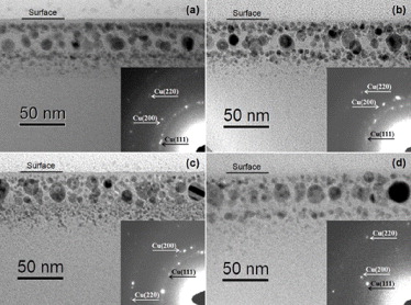
Fig. 2: XTEM micrographs of the Cu and Cu + 1.0Zn samples. (a) and (b): the Cu sample before and after 400 °C annealing: (c) and (d): the Cu + 1.0Zn sample before and after 400 °C annealing. The corresponding SAED pattern is inserted in each image.
Download figure:
Standard imageAs for the Cu + 1.0Zn sample, XTEM observations show that post Zn ion implantation results in formation of hollow NPs in large quantity (fig. 2(c)). Moreover, the average diameter slightly increases to 7.3 ± 3.9 nm as compared with that in the Cu sample. The size increase of NPs is mainly due to the ion beam heating during subsequent Zn ion implantation. Subsequent annealing at 400 °C induces further increase in the average diameter of the NPs (8.5 ± 4.4 nm) accompanied with shrinkage of nanovoids in NPs (see fig. 2(d)). In addition, results from the SAED measurements demonstrate that the formed NPs in both cases are mainly fcc copper (see the inserted images in fig. 2(c) and (d)).
Earlier researches have demonstrated that several factors, such as shape, size and distribution, structure, composition, volume fraction, matrix, etc., could influence the optical properties of the NPs [4, 16]. According to our XTEM observations, the post Zn ion implantation can slightly increase the average diameter of Cu NPs along with their volume fraction. Based on Mie theory of the scattering of electromagnetic wave by a collection of metal spheres suspended in a dielectric medium, SPR wavelengths change very modestly for all the cluster dimensions less than 10 nm [17]. Further, a comparison between SPR absorptions of the Cu sample before and after annealing in fig. 1 also tells us that the slightly increased average size and volume fraction of Cu NPs (refer to figs. 2(a) and (b)) only induce small change of SPR peak in intensity and position. Therefore, the greatly enhanced absorption signal around 561.0 nm for the Cu + 1.0Zn sample can not mainly attributed to the changes in size and volume fraction of the formed Cu NPs, and other factors should be focused on.
During post Zn ion implantation into SiO2 layer involved Cu NPs, the following effects could be expected. Firstly, energetic Zn ions can produce lots of vacancy-type defects in the already formed Cu NPs, which can aggregate to form nanovoids, as revealed by XTEM observations (fig. 2(c)). The formation of hollow Cu NPs generally results in redshift of the corresponding SPR absorption [18–19]. Subsequent annealing gives rise to shrinkage of nanovoids in NPs, causing an evident blue shift of the absorption signal. In our case, although shrinkage of nanovoids in NPs have been observed in the Cu + 1.0Zn sample after 400 °C annealing (fig. 2(d)), no blueshift but large redshift is exhibited by the absorption signal (fig. 1). Therefore, large redshift of the Cu SPR absorption should not be related to the evolution of hollow NPs. Secondly, Zn ion implantation could break up the silica bonds and release oxygen atoms [20]. Then the released oxygen atoms in the substrate can interact with Zn or Cu atoms to form Zn or Cu oxides [17, 21], even Zn2SiO4 in the O-rich region [22], which would change the localized dielectric constant around Cu NPs in the matrix. According to the difference in electronegative values of metal elements (1.90 for Cu vs. 1.65 for Zn) [21, 23], the presence of Zn in layer of NPs could reduce Cu atoms to oxidize. Consequently more Cu atoms could take part in aggregation of Cu NPs. Actually, it has been reported that the lowest concentration of Zn (5%) is sufficient to provide a chemical protection to prevent the oxidation of Cu NPs [10]. Thirdly, during Zn ion implantation, Zn ions will disperse into SiO2 substrate and Cu NPs. By using EDXS analyses, the Zn distribution has been characterized. The typical results are given in fig. 3. From the figure, it is clear that Zn in both NPs and surrounding matrix has been detected. The introduction of Zn atoms at low content into Cu NPs could lead to shift of the absorption signal toward the lower wavelength than that of the pure Cu NPs [10]. The dispersed Zn atoms around NPs could increase the partial dielectric constant of the surrounding matrix, resulting in an enhancement of SPR absorption along with a position redshift [4]. As a result of collective contribution of the above two factors, the Cu + 1.0Zn sample could present an intense SPR absorption at about 561.0 nm as shown in fig. 1(a). With regard to the shoulder band centered at about 430.0 nm, it may originate from the interband absorption of Cu NPs [24]. After 400 °C annealing, as demonstrated in fig. 4, the Zn atoms in Cu NPs diffuse toward the edges of NPs, or even disperse in the substrate. In the case of low Zn concentration, the outward diffusion of Zn atoms in large Cu NPs at such low temperature probably results from a preferential extraction (or oxidation) of Zn element due to the difference in electronegative values of Cu and Zn. As for small Cu NPs containing Zn atoms, their decomposition can be attributed to lower melting point [25] as well as different diffusivities of Cu and Zn atoms in SiO2 [11]. Owing to the decrease of Zn content in Cu NPs, again noting the slight increase of volume fraction of colloids due to thermal growth of NPs (see fig. 2(d)), it can be expected that the corresponding SPR absorption is further enhanced and shifted to a longer wavelength as presented in fig. 1(b). Moreover, it is possible to form a Zn-rich shell around Cu NP due to the outward diffusion of Zn atoms, but this shell should be very thin or even unclosed because of the quite low Zn concentration in Cu NPs. As to the effect of the Zn-rich shell on the Cu SPR absorption, in our opinion, it can be neglected, as discussed in the following.
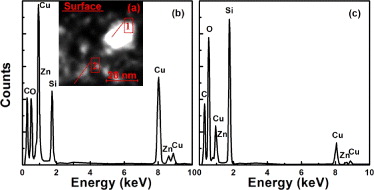
Fig. 3: (Colour on-line) (a) High-angle angular dark-field image for the Cu + 1.0Zn sample before annealing; EDXS spectra recorded (b) inside one of the NPs (spot 1 in (a)) and (c) in the matrix (spot 2 in (a)).
Download figure:
Standard image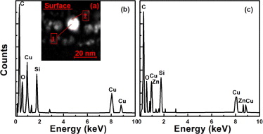
Fig. 4: (Colour-online) (a) High-angle angular dark-field image for the Cu + 1.0Zn sample after 400 °C annealing; EDXS spectra recorded for one NP, (b) central region (spot 1 in (a)) and (c) marginal area (spot 2 in (a)).
Download figure:
Standard imageOptical absorption cross-section σ of a collection of uniform spheres, very small compared to the wavelength λ of incident light and embedded in a medium of dielectric constant εm (i.e., the refractive index is  ), can be well described by Mie scattering theory in the dipole approximation and is given as [26]
where, V0 is the cluster volume, and ε(λ, R) = ε1(λ, R) + iε2(λ, R) is the size- and wavelength-dependent complex dielectric function of the cluster. The absorption cross-section has a maximum value at the SPR frequency, where ε1 + 2εm = 0. The Mie calculations of the absorption cross-section for an individual Cu NP with a diameter of 8.5 nm embedded in SiO2 and ZnO substrates are shown in fig. 5(a). One can see from the figure that a broad and weak peak appears around 570 nm for the SiO2 matrix, while a significantly enhanced peak stands at about 600 nm for the ZnO substrate. When we consider the refractive index of the substrate as n = 1.73, the simulated spectrum shows an enhanced SPR peak of Cu NPs at about 585 nm, which is very similar to our experimental result. Further, by using the algorithms proposed by Toon and Ackerman [27], absorption cross-section spectra of Cu-Zn core-shell NP with a diameter of 8.5 nm embedded in SiO2 and ZnO substrates were also calculated for shell thicknesst of 0.7 and 1.0 nm, approximately corresponding to shells with three and four Zn atomic layers, respectively, as estimated by using the lattice constants of hexagonal-close-packed Zn. The calculated spectra are given in fig. 5(b), which are quite different from those shown in fig. 1(b). Based on the above calculations, it can be concluded in principle that the increased partial dielectric constant of the surrounding matrix of Cu NPs is the main contributor to the significantly enhanced Cu SPR peak at a longer wavelength.
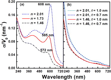
Fig. 5: (Colour on-line) Absorption cross-section σ calculated for (a) Cu NP in SiO2 (n = 1.46), ZnO (n = 2.01) and a matrix with n = 1.73 by using Mie theory, and (b) Cu-Zn core-shell NP with different shell thickness t in SiO2 and ZnO. The diameter of NP is set as 8.5 nm.
Download figure:
Standard imageFor the Cu + 0.5Zn sample, the behaviors of absorption spectra are similar to those for the Cu + 1.0Zn sample before and after annealing as shown in fig. 1. However, due to the lower content of Zn, the variation of partial dielectric constant is not so significant that the enhancement and shift of Cu SPR peak are not so dramatic.
Conclusions
The SPR peak of Cu NPs embedded in silica can be enhanced by post 50 keV Zn ion implantation and subsequent annealing in nitrogen ambient. Especially, remarkable enhancement and shift in SPR peak of Cu NPs have been observed for the sample implanted with Zn ion at fluence of 1.0 × 10¹⁶ ions/cm2 after annealing. The modification in optical absorption of Cu NPs has been demonstrated to be mainly attributed to the increase of partial dielectric constant around the Cu NPs in the matrix. The finding provides a method to dramatically modify the SPR absorption signal of Cu NPs embedded in SiO2.
Acknowledgement
This work is supported by the National Natural Science Foundation of China (Grant No. 11175129), the Natural Science Foundation of Tianjin (Grant No. 12JCZDJC26900) and the Key Laboratory of Beam Technology and Material Modification of Ministry of Education, Beijing Normal University.