
Abstract
Texturing of Ga-doped ZnO (GZO) was performed for Si thin film solar cell applications using the acetic acid-diluted nitric acid solution. The nitric acid-based texturing solution resulted in rougher surface morphology than the HCl solution that has been generally used as a texturing solution of ZnO-based transparent conductive oxides. The highest solar cell conversion efficiency was achieved using 400 nm-etched GZO film. The short circuit current density and conversion efficiency of the single junction a-Si:H solar cell were improved considerably by as much as 28 and 42%, respectively, compared to those of reference cells.
Export citation and abstract BibTeX RIS
When sunlight is irradiated to hydrogenated amorphous silicon (a-Si:H) thin film solar cells through a glass substrate, the rough morphology of transparent conductive oxide (TCO) films causes light scattering at the TCO/a-Si:H interface. Accordingly, extended optical paths of the scattered photons reinforce the photo-induced carrier generation in the light absorption layer. The enhanced light trapping results in the improvement of the short-circuit current density (Jsc) and conversion efficiency (η) of solar cells.1,2 Especially for a-Si:H solar cells, the texturing of the substrate or TCO film is essential to improve the light conversion efficiency because the light absorption coefficient of a-Si:H is smaller than those of CdTe and CuInSe2.3,4
Zinc oxide (ZnO)-based TCOs, such as Ga-, Al-, or B-doped ZnO, have been used as transparent electrodes of a-Si:H solar cells with superstrate structure because of their chemical stability in H2 plasma, high transparency, and high conductivity.5,7 For texturing ZnO-based TCOs, HCl solution has been commonly used as a texturing agent.1,2,8,9 Meanwhile, new texturing agents showing more efficient or more controllable characteristics than HCl solution have rarely been developed. In the present work, a texturing solution, acetic acid-diluted nitric acid (ADN), was newly utilized for texturing Ga-doped ZnO (GZO) TCO film for a-Si:H thin film solar cell applications. In aqueous etching solutions containing HCl or HNO3, the ZnO film dissolves as the aqueous H+ ions attack the oxygen, producing soluble salts as follows:

In this work, the GZO films were deposited on mirror-polished Si wafers or sodium-free glasses by using RF-magnetron sputter deposition. The deposition condition of GZO films has been presented in detail in a previous work.10 The GZO films were textured by varying the loss of GZO films. Here, the 'loss of film' denotes the decrease of film thickness due to texturing and was calculated from the increase of sheet resistance (Rs) due to texturing because Rs is determined by the resistivity and remaining film thickness.1 The sheet resistance was measured by a four-point probe. The samples on Si substrates were used for measuring specular reflectance by a UV-spectrophotometer (U3501, Hitachi, Ltd). Note that the decrease of specular reflectance means higher diffusion of light since the detector perceives only specularly reflected light from GZO samples. The reason why we use a mirror-polished Si substrate in this experiment is to compare the relative reflectance values, which are related to the light scattering effect. The haze ratio of GZO films on glass was measured using a hazemeter (HM-150, Murakami Color Research Laboratory) with light of 550 nm wavelength.
Textured GZO films having different surface roughness were also prepared using ADN solution as transparent electrodes to determine the effect of surface roughness on photocurrent generation of a-Si:H films. The light trapping effect of textured GZO on the performance of a-Si:H single junction solar cells was also investigated.
Amorphous silicon films were deposited by using the plasma enhanced chemical vapour deposition (PECVD) technique. The sample structure for photo-induced current measurement was a textured GZO/a-Si:H (400 nm)/Al electrode. Then, a-Si:H single junction thin film solar cells were fabricated on the textured GZO glasses to show the light trapping effect of textured GZO film. Here, 25 nm p-type a-Si:H was used as a p-window layer, and the cell structure was not fully optimized for high efficiency. The cell area was 0.25 cm2, and performances were measured under AM 1.5 light illumination. The final thickness of textured GZO film, used for measuring the photocurrent density and cell performance, was set to 800 nm to compare the results with untextured 800-nm-thick GZO films. In a previous work, the 800-nm-thick GZO film showed the highest figure of merit value in view of transmittance and conductivity.10
Table 1 shows the haze ratio of GZO film textured using ADN solution in comparison with that of HCl solution. The haze ratio is one of the primary factors to determine the light scattering of TCO,1,11,12 and tends to increase with increasing surface roughness. The increase of the haze ratio of TCO is known to cause the enhancement of the Jsc of solar cells.11,13,14 Table 1 shows that ADN induced larger root-mean-square roughness (Rrms) and haze ratio values than HCl with the same loss of films, 200 nm. The development of roughness through etching is generally known to be caused by the different etch-rates of grains and grain boundaries in polycrystalline film. The addition of acetic acid to the nitric acid solution is thought to increase the etch selectivity to the grain boundaries compared to the grains because grain boundaries react with etching solutions faster than grains. Figure 1 shows SEM and AFM images of GZO films textured using HCl and ADN solutions. Figures 1a and 1b show cross-sectional and plan-view SEM images of a GZO film textured using HCl solution, and Figs. 1d–1e show SEM images of a film textured using ADN solution. As the images illustrate, the film textured by ADN shows more uniformly formed craters and a rougher surface than that of HCl. The AFM data in Figs. 1c and 1f also indicated that the film textured by ADN revealed higher roughness (Rrms = 68.2 nm) than that of HCl solution (Rrms = 53.5 nm).
Table I. Comparison of texturing characteristics. The thickness of GZO films was 800 nm after texturing.
| Loss of film | Rrms | Haze ratio | |
|---|---|---|---|
| Film | (nm) | (nm) | (%) |
| Non-textured 800 nm GZO film | 0 | 6.63 | 0.3 |
| 800 nm GZO film | |||
| GZO film textured by HCl | 200 | 53.53 | 19.4 |
| GZO film textured by ADN | 200 | 68.16 | 25.5 |
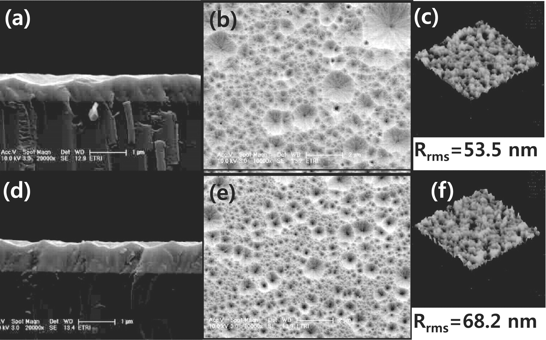
Figure 1. SEM images and AFM results of 200 nm-textured GZO films. (a) and (d) surface SEM images, (b) and (e) cross-section images, and (c) and (f) AFM results of GZO films textured by HCl and ADN, respectively.
Figure 2 shows that the reflectance from the GZO film after texturing with respect to the loss of films. Greater loss of films is inevitable to obtain the same reflectance when using HCl, as shown in Fig. 2. To obtain a reflectance of approximately 6%, 550 nm GZO should be etched by HCl solution in contrast to ADN solution requiring only a 150-nm etch of GZO.
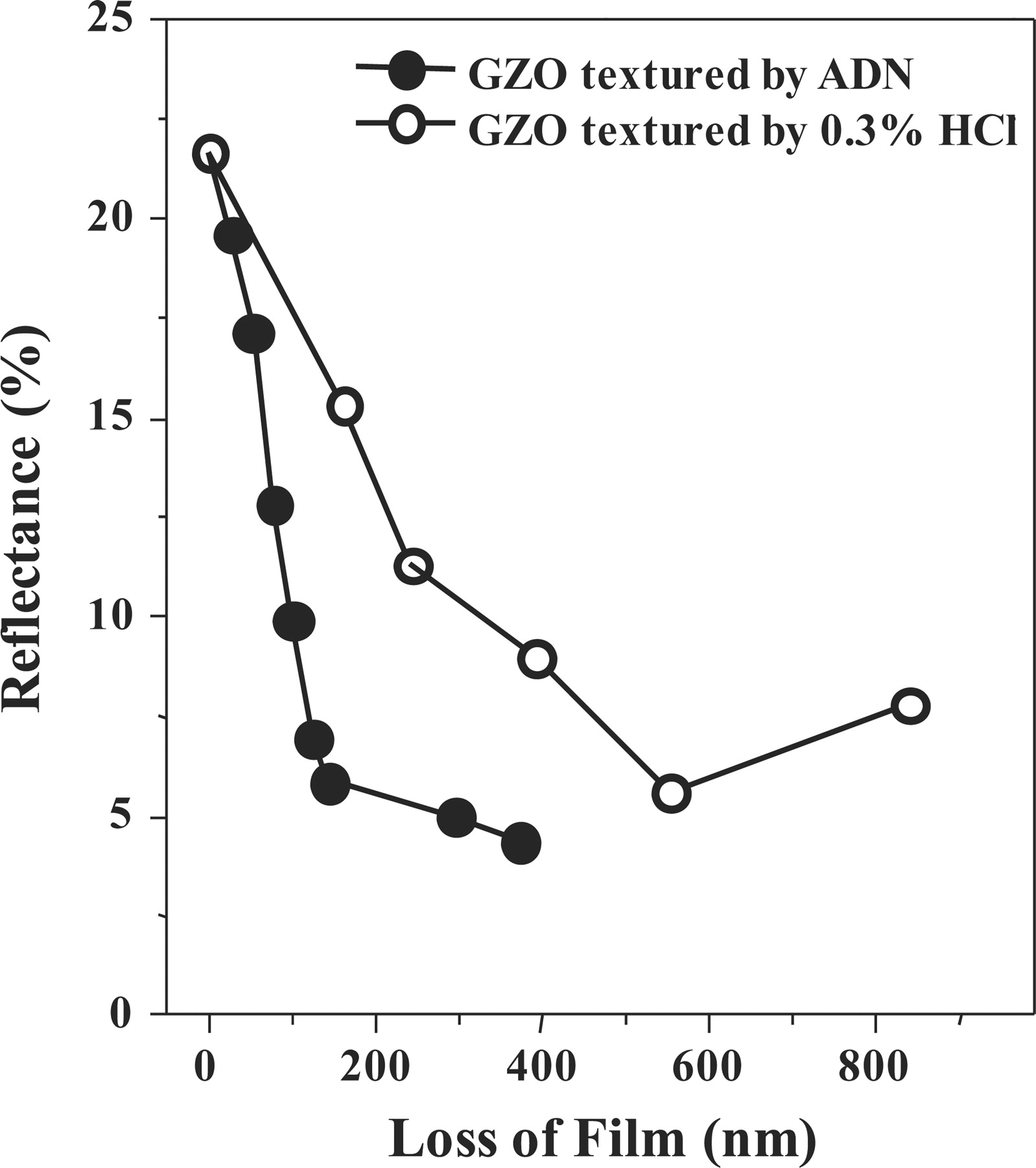
Figure 2. Comparison of reflectance values according to the variation in loss of films using two different texturing agents. The initial thicknesses of GZO films were 1 μm.
Figure 3 illustrates the development of the surface structure of a GZO film as texturing is done using ADN solution. The initial thickness of the film was 1.4 μm. Figure 3a shows SEM photographs of the GZO surface before texturing. Figures 3b and 3c show that the size of craters increased with etch time. Then, an over-etched area, where the glass substrate was exposed, appeared in the sample etched by 1,080 nm, as shown in Fig. 3d.
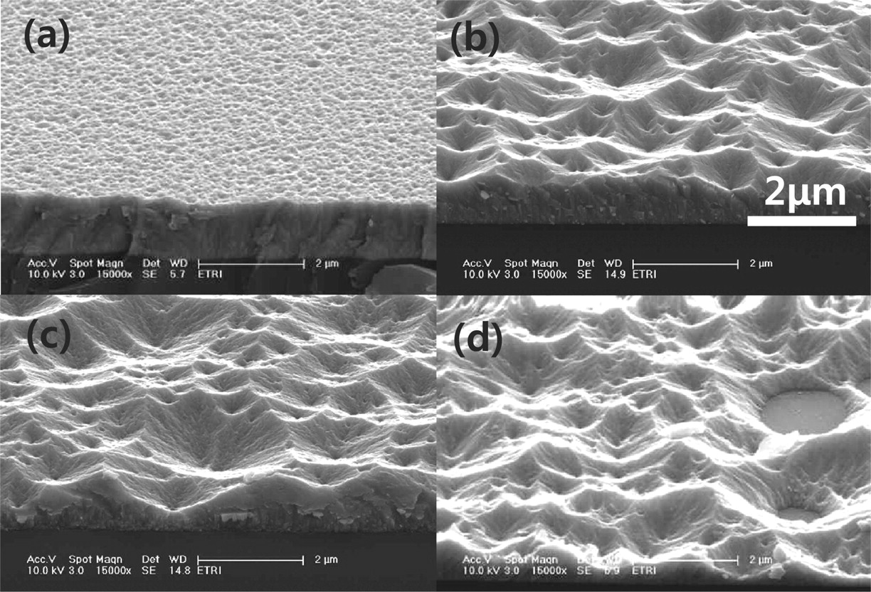
Figure 3. SEM images of GZO films. 1.4 μm GZO films were (a) 0-, (b) 380-, (c) 820-, and 1080-nm-etched.
The dependence of Rrms on the loss of GZO film is shown in Fig. 4. For this experiment, 1.2 μm GZO (TF-C group), 1.4 μm GZO (TF-D group), and 1.8 μm (TF-E group) films were prepared. Before the over-textured region, Rrms increased with an increase in the loss of film. The over-etched region denoted by dashed lines can be defined as the region where the substrate is exposed (see Fig. 3d) and then Rrms decreases. Textured TF-C film shows the largest Rrms of 101 nm when it is textured by 400 nm, and the maximum roughnesses of the other samples (TF-D, and TF-E groups) were a little lower than 100 nm. The results indicate that the roughness of approximately 100 nm is the maximum roughness that can be obtained from textured GZO films in this work.
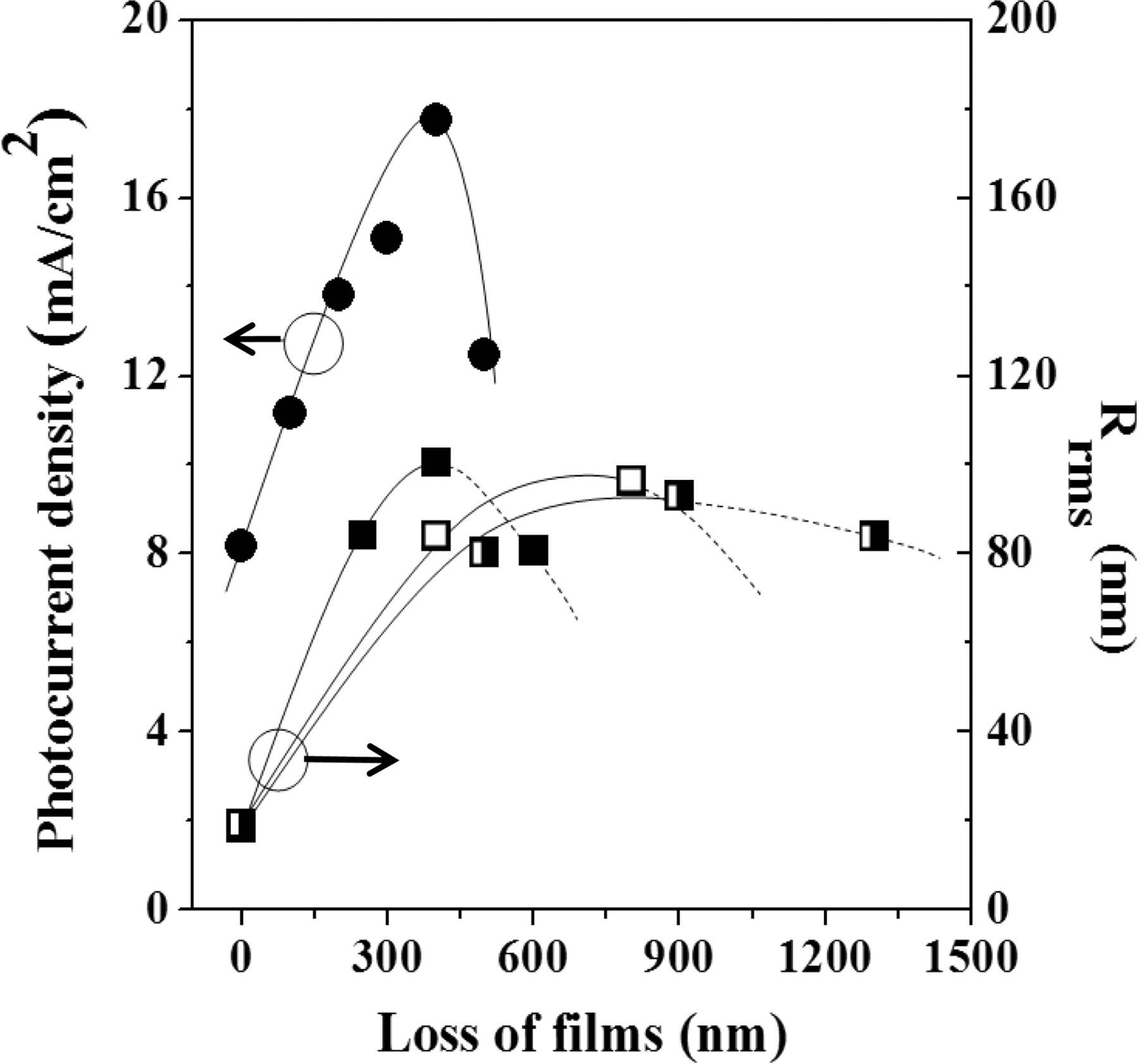
Figure 4. Photo induced current density values (filled circles) and Rrms values of TF-C (filled square), TF-D (open square), and TF-E (half-filled square). The over-textured region (dashed line) was defined by the decrease of Rrms.
The dependence of the photocurrent generation of a-Si:H film on Rrms of a GZO substrate was also investigated for textured GZO films, which were prepared to have a final thickness of 800 nm. The maximum photocurrent could also be obtained from the a-Si:H film deposited on 400 nm-etched GZO showing the largest Rrms, as shown in Fig. 4. The photocurrent density was 17.8 mA/cm2, which was 2.2 times larger than that of non-textured GZO. When GZO film (initial thickness = 1.3 μm) was 500-nm etched, the a-Si:H film deposited on the textured GZO film showed a decrease in photocurrent. It is presumed that the overetched area, illustrated in Fig. 3d, began to appear and had negative effects on the carrier collection of the GZO film.
To verify the effect of GZO texturing on photocurrent generation in a photovoltaic device, a-Si:H single junction solar cells (the cell configuration is shown as an inset in Fig. 5), 0.25 cm2 in area, were fabricated, and the performance was evaluated. The result is plotted in Fig. 5 with respect to the loss of GZO films. The Voc reduced slightly with increased loss of GZO films. The slight decrease in Voc may be due to the increased carrier recombination rate at the rough interface of TCO and the p-Si:H layer.2,11 The fill factor (FF) of the solar cells fabricated on textured TCO was improved compared to that on non-textured TCO. It is assumed that the carrier collection rate is improved by texturing. However, the FF shows no significant dependence on texturing time as long as it was textured. The Jsc and η show the largest values of 16.30 mA/cm2 and 7.08%, respectively, for the solar cell fabricated on the 400-nm-etched GZO substrate. Among the parameters, the largest increase of Jsc for the sample indicates that the efficiency was enhanced mostly by effective light capturing due to the GZO substrate of the highest roughness. This explanation is also supported by the fact that the Jsc and η follow the same trend. The cells adopting over-textured TCOs revealed a decrease in Jsc and η. It is implied that the exposed perforations behave as defects in the case of a-Si:H solar cells because the carrier diffusion length is very short in the a-Si:H film15 and most carriers generated near the defects will never reach the GZO electrode.
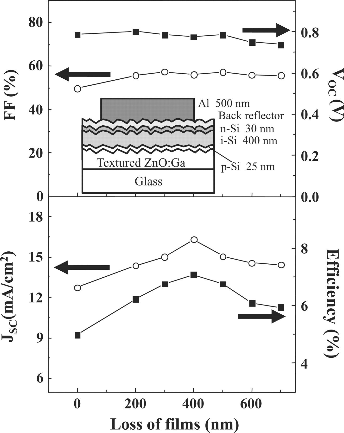
Figure 5. Measured solar cell parameters according to the loss of films. The cell area was 0.25 cm2. The thickness of all the textured films was set to 800 nm.
In the present work, an effective TCO texturing agent, ADN solution, was investigated for the use of a-Si:H thin film solar cell. The results showed that the agent newly applied to the solar cell enables more selective grain boundary etching and induces rougher surface morphology than conventional HCl solution. When 1.2 μm GZO film was 400-nm-textured by ADN, the largest Rrms value of 101 nm was obtained and the highest photocurrent was generated from a-Si:H film on the GZO substrate. The best cell performance was also obtained from the sample on the textured GZO substrate of the highest roughness. The a-Si:H solar cell showed improvements of 28% for Jsc and 42% for η compared to the cell fabricated on non-textured 800 nm GZO. The results indicate that the ADN solution can be utilized as a promising texturing solution of GZO films for Si:H thin film solar cell applications.
Acknowledgments
This work was supported by the New and Renewable Energy Development Project of the Korea Institute of Energy Technology Evaluation and Planning (KETEP) grant funded by the Korean Government Ministry of Knowledge Economy (Contract No: 2008-N-PV-08-P-03-0-000). The authors also thank Dr. K. –H. Kim for measuring the haze ratio of the textured GZO films.