Abstract
A crack-free, uniform InGaN/GaN light-emitting diode (LED) structure with strain-engineered buffer layer was grown on an 8-inch diameter Si(111) substrate. The full width at half maximum (FWHM) of (002) and (102) ω-scan is 280 and 420 arcsec, respectively. For LED on 8-inch Si, multiple quantum well (MQW) photoluminescence (PL) wavelength uniformity of 0.55% (2.4 nm) has been achieved by using proper curvature engineered wafer carrier. We demonstrated high brightness 1×1 mm2 LED devices utilizing vertical chip process then evaluated their device properties. The electro-optical characteristics of the fabricated vertical LED (VLED) shows around 1 W light output power at 1 A injection current with operating voltage of 4.0 V.
Export citation and abstract BibTeX RIS

This is an open access article distributed under the terms of the Creative Commons Attribution 4.0 License (CC BY, http://creativecommons.org/licenses/by/4.0/), which permits unrestricted reuse of the work in any medium, provided the original work is properly cited.
Group III-nitride semiconductors are attractive materials for optoelectronic and power electronic devices because of their wide band-gap and good thermal-mechanical stabilities. In particular, GaN has been considered as the most important semiconductor next to silicon because of its applications in solid-state lighting (SSL). One of current technical issues on SSL is the manufacturing cost. An LED is responsible for 30–40% of a SSL bulb which the price is more than 5 times higher than that of conventional light bulb. In order to reduce the manufacturing cost of GaN-based light-emitting diodes (LEDs), GaN-on-Si approach has collected more and more industry`s attention because of its cost-effectiveness and scalability.
In spite of these excellent advantages, silicon has not been widely used as a substrate material for GaN growth owing to several structural and mechanical problems. The large lattice mismatch (∼17%) between GaN and silicon leads to a relatively high dislocation density for the GaN-on-Si epiwafer, limiting the performance of LED structures. The large mismatch between GaN and Si in thermal expansion coefficient (∼56%) induces a large tensile stress during the cooling process, which often results in cracked layers that are harmful for device applications.1,2 As the substrate size is scaled up, the requirement of wafer flatness becomes stricter due to the limited tolerance in wafer bow for processing a full wafer. For example, even with same curvature, the bow of 8-inch wafer is 16 times as much as that of 2-inch wafer. In addition, optical loss of the absorbing Si substrate is another barrier for realizing high brightness LEDs compared with those on sapphire or SiC substrates. Si is typically opaque, decreasing the LED efficiency due to the absorption of downward light by the substrate.3
In this study, we demonstrate the growth of high crystalline quality, crack-free, and uniform GaN-based LED structures on 8-inch Si(111) substrates and the fabrication of high brightness devices utilizing vertical-current type chip process.
Experimental
All the GaN structures were grown on 1.5-mm-thick 8-inch Si(111) substrates by 3×8'' metal-organic chemical vapor deposition (MOCVD) system. The Si(111) substrate was annealed in the reactor before epitaxial growth in order to remove the native oxide layer, then an AlN nucleation layer was grown to prevent Ga element from reaction with the Si substrate. A step composition-graded AlGaN buffer layer was then grown to control the stress. After that, Si-doped n-type GaN layer, on top of which was grown a four-period InGaN/GaN multiple-quantum well (MQW) structure followed by a Mg-doped p-type GaN as an active region and cladding layer, respectively. After the epitaxial growth, in situ annealing was carried out in a N2 ambient at 600°C to activate the Mg acceptors. Because the in-plane lattice parameter of GaN is larger than that of AlN, the (Al)GaN layer is under compression. We utilize this compressive strained layer to compensate for the tensile stress introduced during cooling of the wafer to the room temperature after finishing the epitaxial growth. By using this stress compensation method, we achieved flat and crack-free GaN-based structures on Si substrates. In situ curvature measurement was employed to monitor the stress variation during entire growth. The epitaxial wafers were characterized by X-ray diffraction (XRD), atomic force microscopy (AFM), and photoluminescence (PL) mapping.
After evaluation of the 8-inch GaN-on-Si epitaxial wafer, a 1 mm × 1 mm sized, vertical-current type LED (VLED) was fabricated using both wafer bonding and Si removing process, as shown in Fig. 1. The VLED was fabricated as follows. The epitaxial wafers were cleaned in the mixed solution of sulfuric acid (H2SO4) and hydrogen peroxide (H2O2) (2:1) for 5 min to remove both the native oxide and organic contamination. After cleaning process, a Ni/Ag/Ni layer was deposited on top of the p-GaN layer. These multiple layers play a role of the p-ohmic contact layer and a light-reflecting layer at the same time. A 2-μm-thick wafer-bonding layer was then subsequently deposited, which consisted of Au-Sn alloy, and after that the wafer was bonded onto a molybdenum conductive substrate through the thermo-compressing bonding method at 300°C for 30 min. Next, in order to remove the silicon substrate rapidly, the etch of the silicon was performed in ammonium bifluoride (NH4HF2) and nitric acid (HNO3) solution (1:1 mixture) at 50°C for 2 hrs. The NH4HF2 etches silicon about 15 times faster than HF.4,5 The overall etching reaction can be written as follows:


Figure 1. VLED structure fabricated in this work: (a) optical microscopy of VLED chip, and (b) emission distribution of VLED chip at an injection current of 350 mA.
Figure 2 shows the surface morphology of exposed un-doped GaN after removal of silicon substrate via NH4HF2 based etching. Any damage or residual Si was not observed on the surface. The exposed un-doped GaN was then etched away to expose the n-GaN layer using wet and dry etching processes; a square mesa of 1 mm × 1 mm was finally defined by the dry etching method. To enhance the light extraction efficiency, the n-GaN surface was etched using the 5 M dissolved potassium hydroxide (KOH) in water at 60°C for 5 min without any etching mask. Finally, a Cr/Al/Ni/Au layer was deposited onto the textured n-GaN surface as an n-type contact electrode. The fabricated devices were mounted on the standard lead-frame packages and covered with transparent epoxy resins. Current-voltage (I-V) and light output (L-I) measurements were made on the processed LED devices.
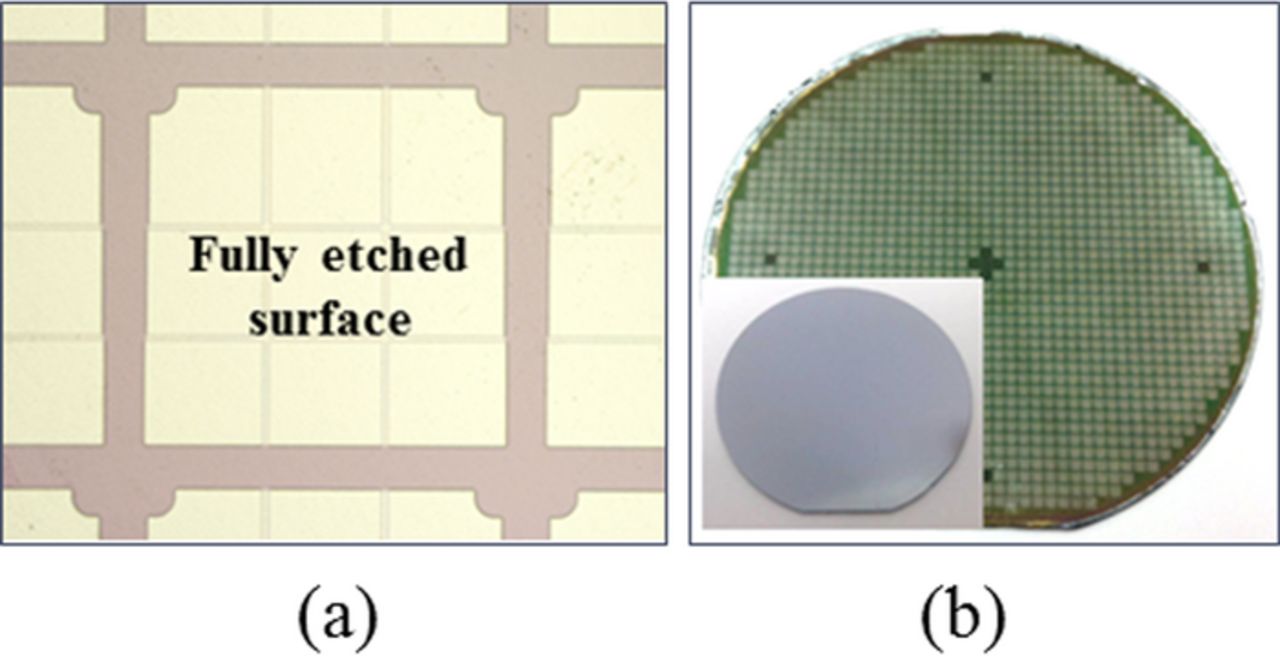
Figure 2. Optical images of (a) the exposed un-doped GaN surface and (b) the LED wafer after removal of Si (The inset is silicon substrate before removal).
Results and Discussion
In order to evaluate the crystal quality of the 8-inch GaN-on-Si based blue LED wafer, we have measured the XRD rocking curves of (002) and (102) planes. The GaN thickness was approximately 4 μm. Figures 3(a) and 3(b) show the rocking curves measured at the center of the wafer. The narrow full width at half maximum (FWHM) values of 280 and 420 arcsec were obtained for (002) and (102) planes, respectively. These values are comparable to the best reported so far for the GaN-on-silicon structure. The surface morphology of GaN layer investigated by an AFM exhibits very smooth surface and shows clear atomic step patterns, as shown in Fig. 4. The root-mean-square (RMS) roughness is 0.15 nm in a 5 × 5 μm2 scanned area. Since In incorporation during the growth of InGaN MQW is highly temperature dependent, it is essential to make uniform growth temperature over the whole wafer in order to get uniform emission wavelength. However, it is difficult to obtain the uniform emission wavelength because of the large bow during the epitaxial growth, resulting in huge temperature difference over the wafer. For the precise bow control, the key is in the control of the compressive strain accumulated during the epitaxial growth at high temperature. Otherwise, the wafer becomes to have a convex shape during the MQW growth, as shown in Fig. 5. Due to the convex shape of the wafer during MQW growth, there is a temperature gradient from center to edge of the wafer. Therefore, properly designed wafer carrier pocket with convex-shaped bottom and edge tabs was employed to minimize the temperature difference over the 8-inch wafer, as shown in Fig. 6. These edge tabs act to minimize direct contact region between wafer and wafer carrier during the growth. The position of tabs is determined to prevent the wafer wobbling caused by the centrifugal force during high speed rotation of susceptor. Thus, as shown in Fig. 7, extremely high emission wavelength uniformity can be obtained with 2-mm edge exclusion of the PL mapping. The standard deviation of the emission wavelength is as small as 2.41 nm, which is 0.55% of the average emission wavelength of 434.7 nm. These are among the lowest values reported to date.
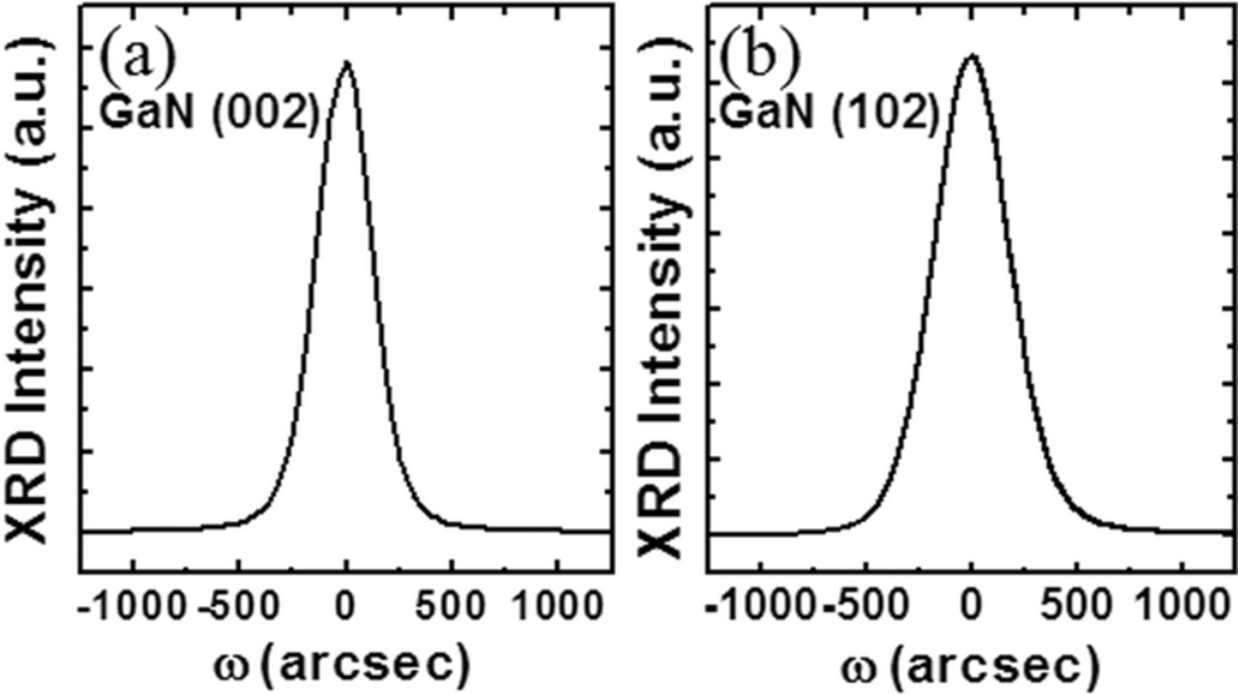
Figure 3. XRD rocking curves of (a) GaN (002) and (b) GaN (102) planes at the center of the 8-inch GaN-on-Si epiwafer.
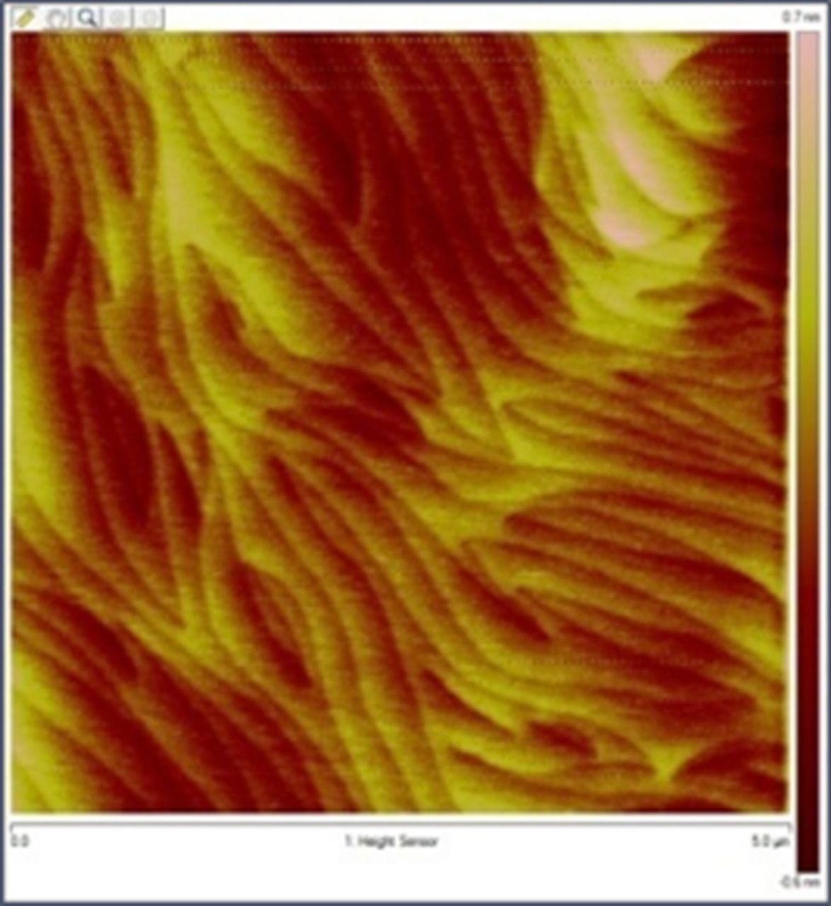
Figure 4. AFM surface morphology (scanning area: (a) 5×5 μm2) of 4-μm-thick GaN epitaxial layer.
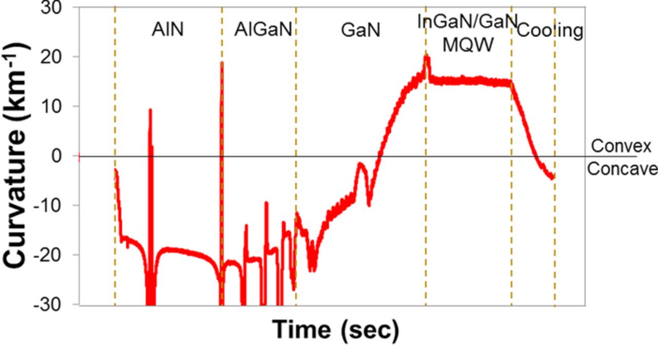
Figure 5. In situ wafer curvature profile measured during the growth of 4.5-μm-thick GaN-based MQW structure on 8-inch Si substrate.
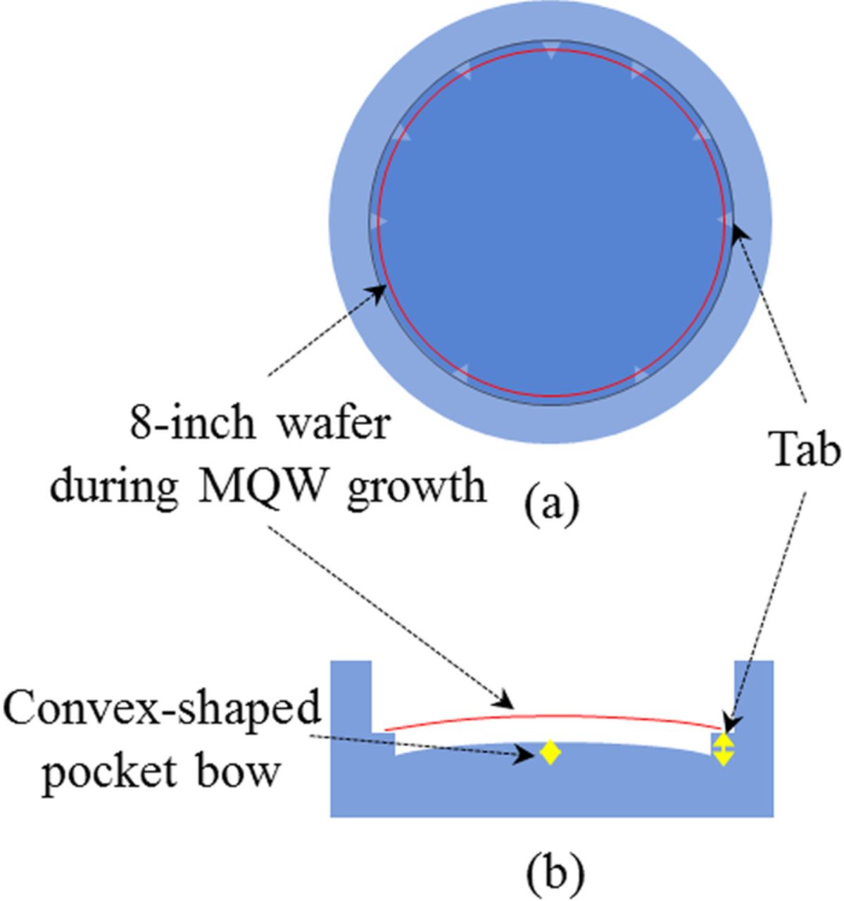
Figure 6. Schematic (a) plan-view and (b) cross-sectional diagrams of wafer loading pocket with convex-shaped bottom and edge tabs designed for uniform wafer temperature in this work.
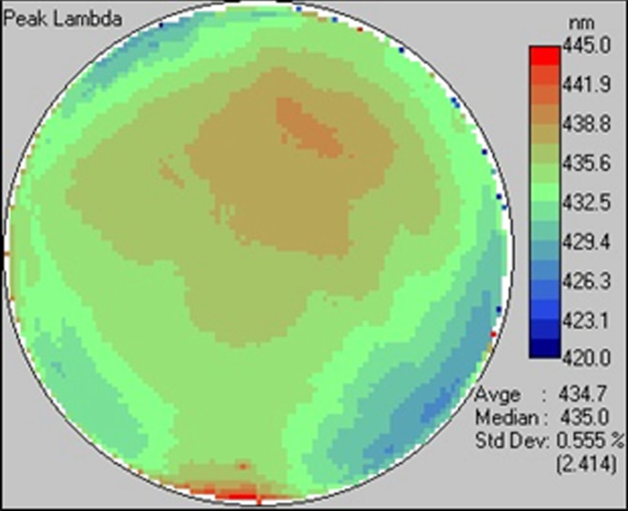
Figure 7. PL mapping of an 8-inch GaN-on-Si based blue LED wafer. The standard deviation of the emission wavelength is as small as 2.41 nm (0.55%).
Besides, Si substrate thickness and Si doping for GaN are the other parameters influencing on the wafer bow. Figure 8 shows the comparison of wafer bow (Fig. 8a) and wavelength uniformity (Fig. 8b) for 6-inch MQW structures with various Si substrate thicknesses from 0.8 to 1.5 mm. The wafer bows during MQW growth were 112, 61, 30, and 19 μm for the substrate thickness of 0.8, 1.0, 1.15, and 1.5 mm, respectively. The standard deviations of the emission wavelength were 7.3, 6.7, 5.5, and 1.5 nm for the substrate thickness of 0.8, 1.0, 1.15, and 1.5 mm, respectively. Thicker the substrate, less is the wafer bow and better is the wavelength uniformity. Figure 9 shows the in situ bow measurement of both undoped GaN (u-GaN) and Si-doped GaN (n-GaN). Thickness and doping concentration of Si doped GaN layer were 2 μm and 8×1018 cm−3, respectively. In contrast with u-GaN, the slope of compressive stress for n-GaN layer was saturated because Si doping induces tensile stress. This rules out that under typical GaN growth conditions, the Fermi level position of highly Si-doped GaN generates vacancies that interact with edge type dislocations inducing dislocation climb and tensile stress, as already reported by Xie et al.6 Therefore we found that the wafer bow significantly depends on the doping concentration and thickness of the Si-doped layer. Thus, the Si substrate thickness and Si doping of the epitaxial layer need to be carefully controlled for achieving the crack-free and uniform GaN-on-Si LED structures.
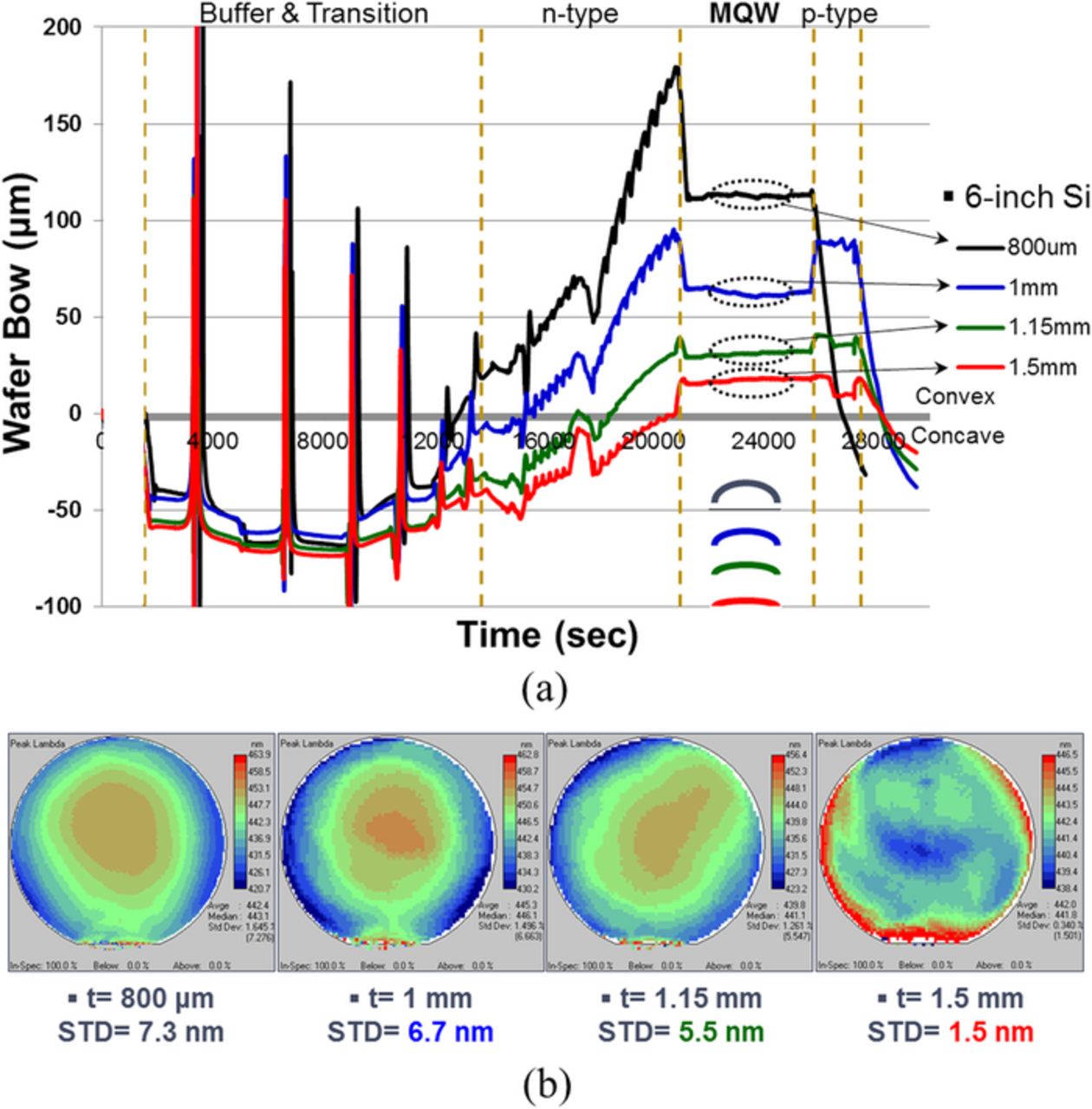
Figure 8. Comparison of (a) wafer bow and (b) wavelength uniformity for GaN-based MQW structures on 6-inch Si with various substrate thicknesses.

Figure 9. Bow measurements of unintentionally doped GaN and n-type GaN doped with Si concentration of 8×1018cm−3.
Figures 10a and 10b show the current-voltage (I-V) and light output (L-I) characteristics of the fabricated VLED in this work. The electro-optical characteristics of a 1 mm × 1 mm sized VLED shows 24.5% wall-plug efficiency (980 mW light power at 1 A injection current) with operating voltage of 4.0 V.
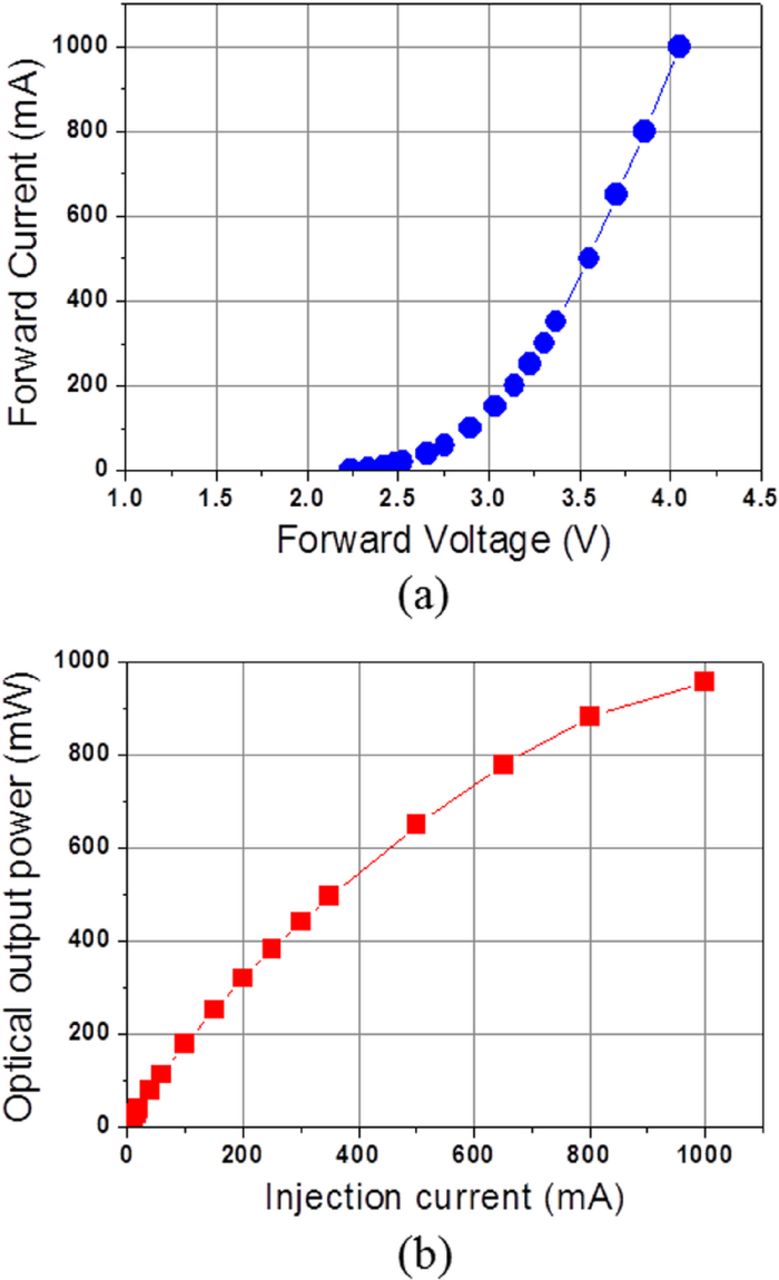
Figure 10. Electro-optical characteristics of VLED (a) current-voltage (b) current-light output power.
Conclusions
We demonstrated the growth of high crystalline quality, crack-free and uniform GaN-based LED structures on 8-inch Si(111) substrates by MOCVD and fabricated high brightness devices utilizing vertical chip process. VLEDs were prepared by substrate transferring technology in combination with wafer bonding process and Si removing process, to enhance the light extraction efficiency and to prevent current crowding effect as well. From a 1 × 1 mm2 VLED chip, the light output power and operating voltage at 1 A drive current are almost 980 mW and 4.0 V, respectively. These results show the promise of Si as a large area, inexpensive substrate for high-efficiency GaN-based LEDs with similar performance to devices on sapphire. Therefore, the GaN-on-Si can provide a new route to the applications of GaN-based high-power and cost-effective solid state lighting.
Acknowledgment
This work was supported by the Industrial Strategic Technology Development Program (14102003): "Development of WPE 75% LED device process and standard evaluation technology", funded by the Korea Ministry of Trade, Industry & Energy (MOTIE).