
Abstract
Hydrogenated intrinsic Si (Si:H) thin films were deposited by a plasma-enhanced chemical vapor deposition technique, and the effect of the SiH4 flow rate ([SiH4]) and hydrogen dilution ratio (R) on the crystalline phase transition was studied using Raman spectroscopy and high-resolution transmission electron microscopy. The crystalline volume fraction (Xc) was strongly affected by [SiH4] as well as R, and higher Xc could be achieved by using a lower [SiH4] at the same R. The dependence of phase transition on the crystallinity of the under-lying layer was also investigated by depositing Si:H films on various substrates. To evaluate the effects of [SiH4] and R on the quality of amorphous-Si:H (a-Si:H) films, etch rates and absorption coefficients were obtained by an H2-plasma etching process and UV-Vis spectrophotometry, respectively. Even under the deposition condition resulting in a-Si:H films, the deposition rate decreased by a factor of 3 to 4.6, and the film density considerably increased as R increased from 4 to 19. On the other hand, the absorption coefficient very slightly decreased with R. The presence of microcrystalline Si:H could be observed only from the samples deposited with R>19 when the film was deposited on amorphous substrate.
Export citation and abstract BibTeX RIS
Numerous efforts have been made to improve the efficiency of hydrogenated amorphous Si (a-Si:H) and microcrystalline Si (μc-Si:H) thin-film solar cells up to the present. The conversion efficiency of a-Si:H thin-film solar cells is principally determined by the structural, optical, and electrical properties of the intrinsic Si film. Si:H films have been generally deposited using a plasma-enhanced plasma deposition (PECVD) technique and these properties strongly depend on deposition parameters, such as the hydrogen dilution ratio (R), the substrate temperature, the flow rate of source gases, the pressure of the deposition chamber, and so on. Therefore, the effects of deposition parameters on the film characteristics and, by extension, on solar cell performance have been studied to enable the fabrication of highly efficient solar cells.
The growth process and the characteristics of a-Si:H and μc-Si:H films have been studied using real-time spectroscopic ellipsometry (RTSE), infrared attenuated total reflection spectroscopy methods,1–3 and Raman spectroscopy.4–6 Previous works reported that the formation of crystalline phase could be engineered by carefully adjusting the R value during the PECVD of Si:H films.7–9 It is also generally known that the deposition rate of Si:H films strongly depends on the deposition conditions, and a-Si:H films are deposited at much higher deposition rate than μc-Si:H films with the PECVD method.8 Therefore, it is important to ascertain the dependence of the deposition rate on parameters such as R and SiH4 flow rate ([SiH4]), as well as the dependence of film quality on the deposition rate. In this work, a-Si:H and μc-Si:H thin films were deposited at various R and [SiH4] using the PECVD method and the dependence of film properties on the deposition parameters was investigated for the crystalline phase engineering of Si:H films. In particular, it is shown that the deposition rate and film density would be changed by several times even within the deposition condition region resulting in the amorphous phase. These changes in the quality of amorphous films are worth noting because the conversion efficiency of a-Si:H thin-film solar cells is significantly affected by the quality of the light absorbing a-Si:H film. The a-Si:H film close to the transition to µc-Si:H, deposited with a deposition rate lower than 1 Å/s, is thought to be a protocrystalline a-Si:H that has been reported to result in high-efficiency a-Si:H thin film solar cells showing a low light-induced degradation.10, 11 The effect of the under-lying layer (substrate) on the crystallinity of Si:H films was also investigated by comparing the crystalline volume fraction (Xc ) of Si:H films deposited on glass and p-type μc-Si film. In this work, the crystalline quality was characterized using Raman spectroscopy. The Raman shift is affected by the vibration of electronic polarization for constituents in the films, which depend on bonding structures, such as atomic distance and bonding angle.12
Experimental
Si:H films were deposited on SiO2-coated Si substrates and sodium-free glasses using PECVD of a parallel-plate reactor to which the 13.56 MHz RF plasma was applied. The SiO2-coated Si substrates were used for film thickness measurement, whereas the glass substrates were used for optical and Raman spectroscopic analyses of Si:H films. Substrate temperature (Tsub), chamber pressure (P), and rf-power were kept constant at 250°C, 1.2 Torr, and 30 W, respectively. Silane (SiH4) diluted with H2 gas was used as the source gas in the deposition of Si:H films. 150nm-thick Si:H films with R ranging from 4 to 49 were prepared by varying [SiH4] from 3 to 50 sccm and varying the H2 flow rate ([H2]) from 20 to 1000 sccm. Here, R was defined by the flow rate ratio of H2 to SiH4, [H2]/[SiH4]. Some of the samples were etched using H2 plasma for 20 min to compare the etch rates of Si:H films deposited under various conditions. The plasma-etching conditions were Tsub = 250°C, P = 1.2 Torr, rf-power = 80 W, and [H2] = 1000 sccm.
The thickness of the samples was measured by an optical measurement device of thin film thickness (Nanospec 9100, Nanomatrix). A UV-Vis spectrophotometer was utilized to obtain the absorbance of Si:H films, and the absorption coefficient was calculated using the absorbance and film thickness. The crystallinity of the films was evaluated using Raman spectroscopy in a back-scattering configuration and with a 514.5 nm Ar-laser as an excitation source. The Raman spectra were deconvoluted into an amorphous Si-related band at 480 cm−1 and crystalline Si-related bands at 520 cm−1 and 500–510 cm−1. For two representative samples, high-resolution transmission electron microscopy (HRTEM) and selected-area electron diffraction (SAED) observations (a JEM-ARM200F, JEOL) were performed to ascertain the crystalline state of Si:H films.
Results and Discussions
Figure 1 shows the deposition rate of Si:H thin films deposited on SiO2/Si substrate with respect to R in the range from 4 to 49. In this experiment, [SiH4] was also varied from 3 to 50 sccm. The deposition rate drastically decreased in spite of the small increase in R from 4 to 9, while there is no significant change in deposition rate in the R range from 24 to 49. In the low dilution region, hydrogen could be incorporated into positions interrupting Si-Si clustering due to the binding energy of Si-H (3–3.6 eV) which is larger than that of Si-Si (2–2.5 eV), and might induce the abrupt decrease of deposition rate. In the high dilution region of R ranging from 24 to 49, the saturation of deposition rate is responsible for the solubility limit of hydrogen in Si:H films.13 It is well known that a higher R inducing a lower deposition rate is more advantageous to obtain Si:H films which have crystalline phase.14 The deposition rate was also affected by [SiH4]. The deposition rate increased with increasing [SiH4] from 3 to 22 sccm, and the maximum deposition rate was obtained at [SiH4] of 22 sccm. Then the deposition rate decreased with further increase of [SiH4]. These results indicate that the deposition rate is significantly affected by [SiH4] even at the same partial pressure of SiH4 and the same total chamber pressure, and there is a critical [SiH4] value showing the maximum deposition rate.
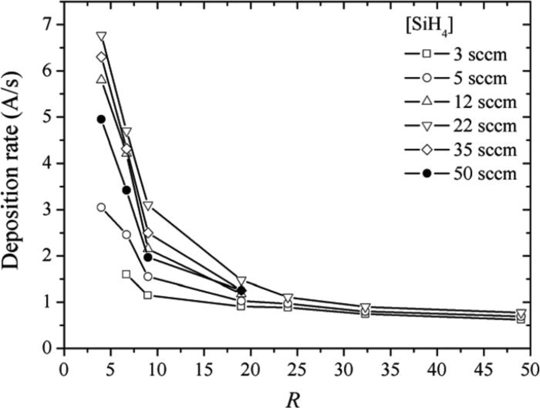
Figure 1. Deposition rate of Si:H thin films deposited by PECVD at various [SiH4].
According to the result in Fig. 1, it might be thought that the phase transition from amorphous to microcrystalline phase occurred in the R region between 4 and 9 in which the deposition rate abruptly decreased. Thus, Raman spectroscopic analysis was carried out to determine the crystalline phase of Si:H films. However, the films deposited at R of 4 and 9 showed only a broad band around 480 cm−1 indicating amorphous phase. The Xc values of the samples deposited at R ranging from 4 to 49 were obtained using Raman spectroscopy and plotted with respect to R in Fig. 2. The method to calculate Xc values is explained in detail in Fig. 3. The data of Fig. 2 indicates that the microcrystalline phase of Si:H film was observed only at R values higher than 19. However, the deposition rate did not show any drastic change in the R region from 19 to 24 as shown in Fig. 1. Therefore, it is not recommended to predict the phase transition by measuring the change of the deposition rate of Si:H film. While a few earlier works have reported the transition between two different phases of a-Si:H films,2 abrupt change in the deposition rate of a-Si:H film has not been reported. Wronski et al. observed the formation of four different crystalline phases of Si:H films during deposition by using RTSE (Ref. 2) and reported that a-Si:H films with unstable and stable surface were deposited at low R values and the transition between these two states near R ∼7 was called 'roughening transition' because the a-Si:H films showed different degrees of surface roughness. The R value for roughening transition depends on the film thickness.
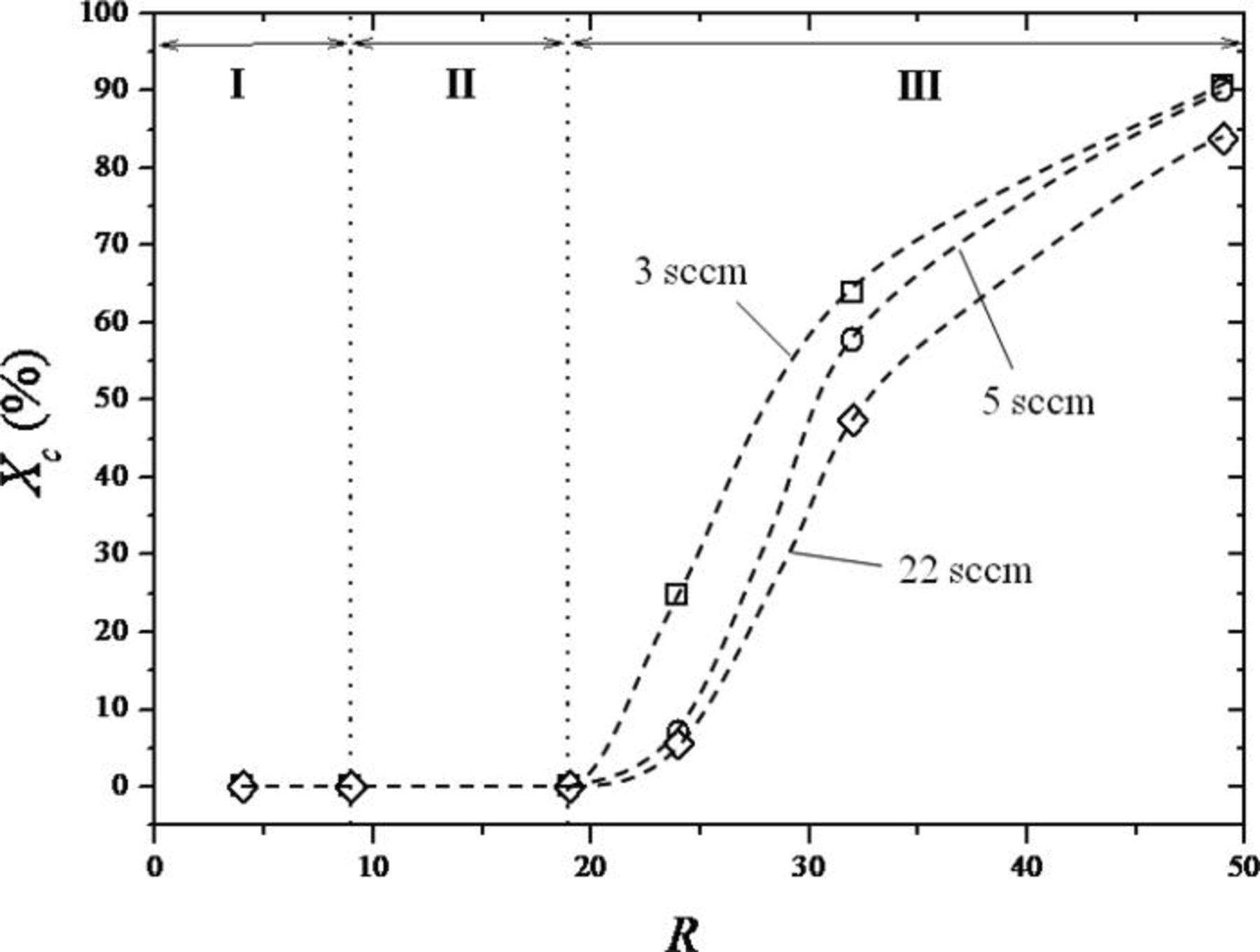
Figure 2. Change of Xc of Si:H thin films deposited at [SiH4] of 3, 5, and 22 sccm.
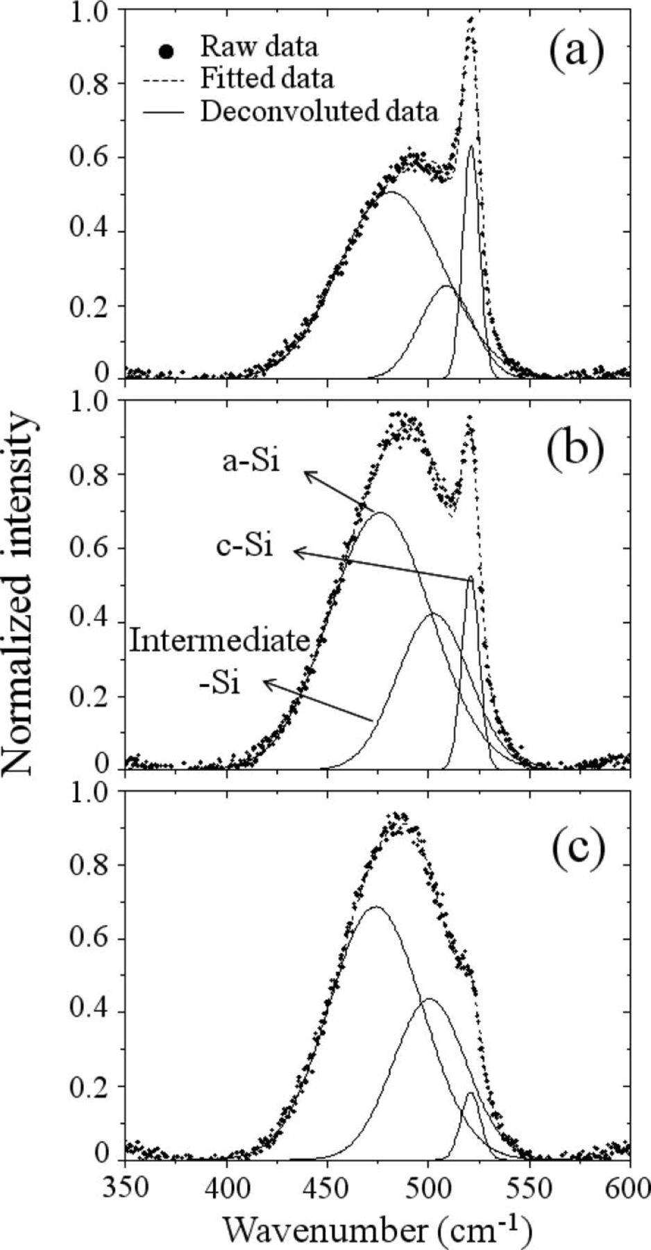
Figure 3. Raman spectra of μc-Si:H thin films deposited at R = 32.3 and their deconvolution results: [SiH4] of (a) 3 sccm, (b) 5 sccm, and (c) 22 sccm.
The microcrystalline phase appears at relatively high R values and single-phase μc-Si:H film could be achieved at very high R values. In the present work, two dotted lines were denoted at R values of 9 and 19 as boundaries of three different regions, I, II, and III, as shown in Fig. 2. One line between regions II and III represents the boundary of crystalline phase transition. On the contrary, the deposition rate of Si:H films in region I decreased more rapidly than in region II and the Xc values of Si:H films deposited at R values up to 19 were zero. These results imply that a transition of film quality would be occur near R = 9. The transition may correspond to the roughening transition mentioned by Wronski.2 In the region of R higher than 19, the Xc values increased with increasing R. Figure 2 also shows the dependence of Xc on [SiH4]. The phase transition took place earlier, that is, at lower R, with smaller [SiH4] as shown in Fig. 2. The higher Xc value was obtained from the Si:H film deposited at the lower [SiH4] due to the higher SiH4 gas depletion effects. The results are consistent with the work of Fltrin et al. , which showed that the microstructure transition width from amorphous to microcrystalline phase strongly depended on the [SiH4], although the phase transition was studied with much lower [SiH4] and in a much higher depletion regime than those of the present work.15
Among the data in Fig. 2, the Raman spectra of mixed phase Si:H films deposited at R of 32.3 with [SiH4] of 3, 5, and 22 sccm, are illustrated in Figs. 3a, 3b and 3c, respectively. To calculate Xc, the Raman spectra were deconvoluted into three different components, crystalline (520 cm−1), amorphous (480 cm−1), and intermediate peaks (500–510 cm−1), using a non-linear fitting method and a Gaussian distribution, as shown in Fig. 3. Here, Xc is defined using the deconvoluted component peaks as16
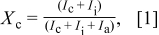
where Ic, Ii, and Ia are the normalized intensities of the crystalline, intermediate, and amorphous peaks, respectively. The calculation using the deconvolution results and Eq. 1 showed that Xc values of the mixed-phase Si:H films of Figs. 3a–3c were 63.8, 57.7, and 47.4%, respectively. The mean crystallite size d also can be estimated from the microcrystalline peaks of Si:H films as5
where B is 2.0 cm−1 nm2, and Δ ω is the frequency shift in unit of centimter, which is the difference between the observed sharp peak frequency value and the single crystal Si peak value of 522 cm−1. With increasing [SiH4] from 3 to 22 sccm, the sharp Raman peak shifted approximately 1 cm−1 toward a lower wave number.17 The crystallite size d was calculated to be 17.3, 7.7, and 4.8 nm for the Si:H film deposited at [SiH4] of 3, 5, and 22 sccm, respectively.
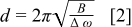
Two representative films were chosen for TEM observation, with the aim to confirm the results of the Raman spectroscopic measurements. Figure 4 shows bright field TEM (left) and HRTEM (right) images of Si:H films deposited at [SiH4] of 5 sccm with R values of 9 and 32.3. The inserts are selected-area electron diffraction (SAED) patterns. While the thickness and crystalline structure of the films could be observed from cross-sectional TEM images, the SAED patterns provided averaged information on the crystalline orientation. In the case of Si:H film with Xc = 57.7% which was deposited at R = 32.3, a crystalline Si region of submicron scale was clearly observed as shown in Fig. 4a. On the other hand, in the case of Si:H film deposited at R of 19, no crystalline region was observed, as shown in Fig. 4b. The µc-Si:H film (Xc = 57.7%) was also confirmed by the intense diffraction rings corresponding to the planes (111), (220), and (311), while only diffused rings were observed from the a-Si:H film, as shown in insets in HRTEM images of Figs. 4a and 4b. These results are consistent with the Raman results. The arrows in Fig. 4a indicate the deposition direction of Si:H film. The longish grains of crystalline size larger than 10 nm were formed along the deposition direction. The crystallite size in Fig. 4a was larger than 7.7 nm and was calculated using Raman data in Fig. 3b, because the Raman peak position revealed the mean crystallite size in the film.
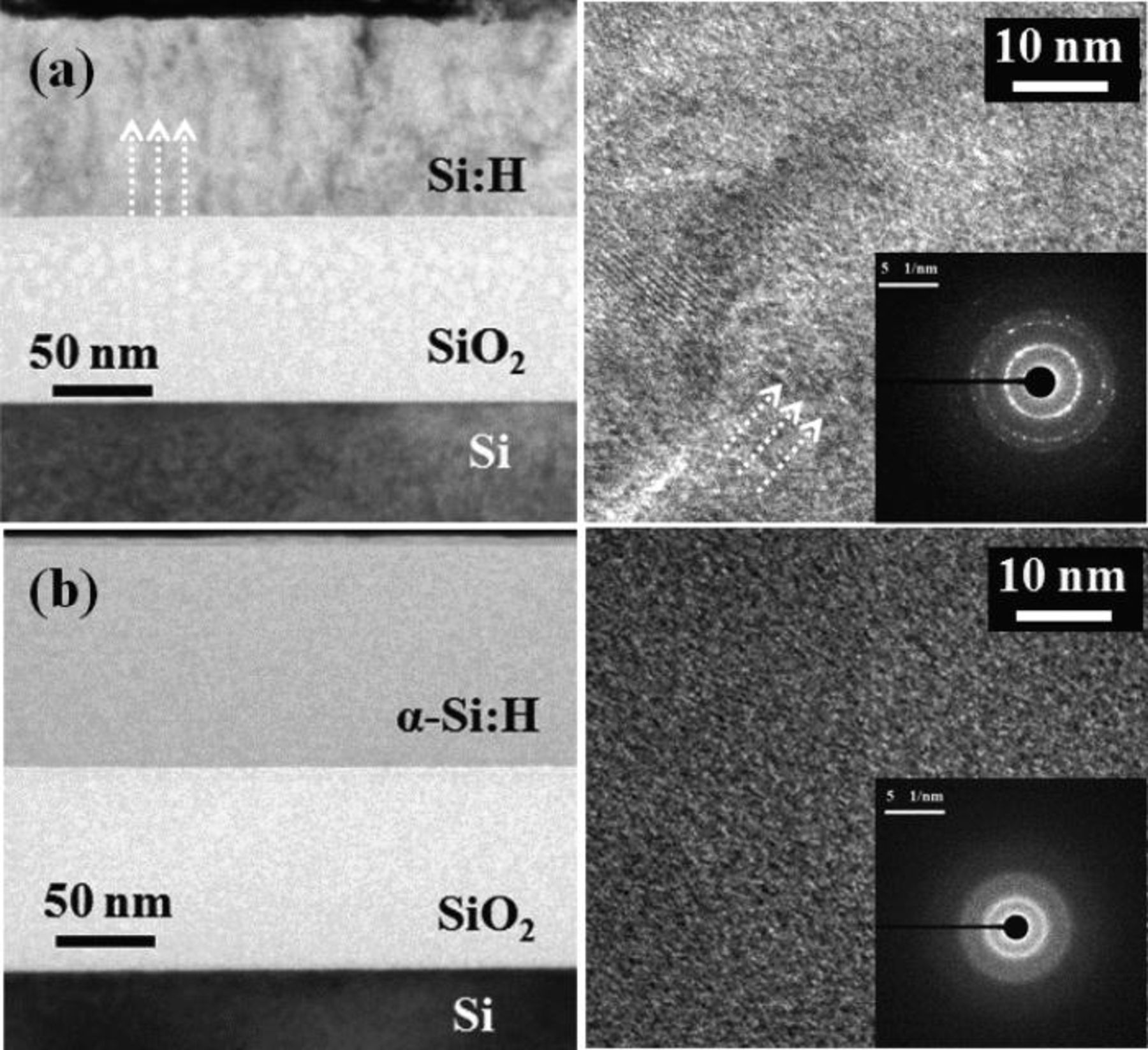
Figure 4. Cross-sectional bright field TEM (left) and HRTEM (right) images of Si:H films deposited at [SiH4] = 5 sccm with R of (a) 32.3 and (b) 19. The SAED patterns are shown in the inserts of the HRTEM images.
To evaluate the effects of [SiH4] on the density of a-Si:H films deposited at R ranging from 4 to 19, H2-plasma etching was carried out for 20 min. Generally, the etch rate of a film is affected by its packing density. Figure 5 shows the etch rate of the a-Si:H films deposited with [SiH4] of 5, 22, and 50 sccm with respect to R. The etch rate decreased with increasing R in the deposition process. From these results and Fig. 1, we can deduce that the a-Si:H films deposited with higher R formed denser films resulting in lower deposition rates. The etch rate was affected by the [SiH4] as well as R. The a-Si films deposited at [SiH4] = 22 sccm showed the highest etch rate in all the R values due to the highest deposition rate. It was also observed that the etch rate decreased with a steep slope in the R region from 4 to 9, while it gradually decreased in the R ranging from 9 to 19. Theses R ranges correspond to region I and II in Fig. 2 because all the Si:H films in this region are amorphous. The change of etch rate following the same trend as the deposition rate indicates that the film quality determining the deposition rate was the film packing density rather than the crystallinity of the films.

Figure 5. Etch rate of a-Si:H thin films deposited by PECVD at [SiH4] of 5, 22, and 50 sccm.
UV-Vis transmittance spectra of the Si:H films were also studied to determine the optical absorption coefficient. Figure 6 shows the dependence of the absorption coefficient at photon energy of 2.5 eV on [SiH4] in the range from 3 to 50 sccm. It has been reported that the absorption coefficient decreased as Xc increases.18 In this work, the absorption coefficient of Si:H films in regions I and II (amorphous region) slightly decreased as R increased from 4 to 19, and the highest absorption coefficient was obtained at [SiH4] = 22 sccm, at which point, the highest deposition rate was obtained. However, the change of absorption coefficient followed the trend of crystalline phase formation rather than that of deposition rate with respect to R, and the absorption coefficient in region III rapidly decreased with increasing R. That is because the absorption coefficient is mainly related to the crystalline state of the Si:H films.
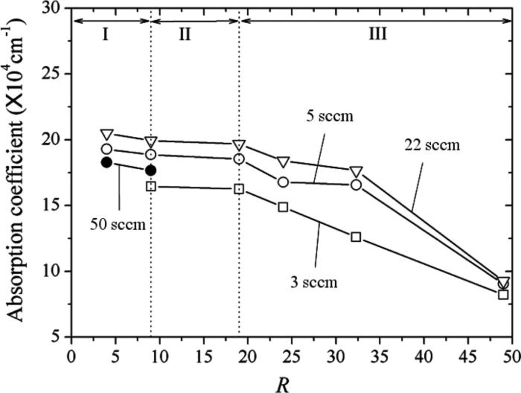
Figure 6. Dependence of the absorption coefficient at photon energy of 2.5 eV on R with [SiH4]: 3, 5, 22, and 50 sccm.
All the samples discussed above were deposited on sodium-free glass substrate. However, the intrinsic a-Si:H or μc-Si:H films were practically deposited on microcrystalline p- or n-type Si:H thin film in a p-i-n or n-i-p solar cell structure.19 Thus, we deposited the intrinsic Si:H films at R from 9 to 32.3 on 25 nm-thick p-type μc-Si:H films (Xc = 76.5%), and then evaluated the crystallinity using Raman spectroscopy. Si:H films deposited on p-μc-Si:H layer and glass at R of 9 showed only amorphous phase. Figures 7a and 7b show Raman spectra of Si:H films deposited at R of 19 and 32.3, respectively. At R of 19, the film deposited on glass showed only a broad band around 480 cm−1 indicating amorphous phase. On the contrary, the film deposited on p-µc-Si:H layer revealed a shoulder peak around 520 cm−1 at R of 19. The Si:H film deposited on p-μc-Si:H layer at R of 32.3 shows the effect of the microcrystalline substrate on the development of µc-Si:H (520 cm−1) more clearly. Figure 7c shows the change in Xc of Si:H thin films deposited with [SiH4] of 5 sccm on various substrates. Note that the Si:H film deposited with R = 19 on p-type μc-Si thin film showed Xc of 4.2%, while the Si:H film deposited on glass substrate was amorphous. It was also observed that higher Xc was achieved for films deposited on p-type μc-Si thin film compared to those deposited on glass substrate in region III. Consequently, the R value leading to the phase transition shifted toward the lower R side, and the μc-Si:H thin film could be deposited at a lower R on the crystalline substrate than the amorphous substrate. Therefore, the phase transition of the intrinsic Si:H layer depending on the condition of underlying layer should be considered in fabricating a-Si:H thin film-based p-i-n or n-i-p solar cells.
Figure 7. Raman spectra of Si:H thin films deposited on glass and p-type μc-Si:H film at R of (a) 19 and (b) 32.3 (c) Change in Xc of Si:H films deposited on glass and p-type μc-Si:H film with respect to R.
Summary
In the present work, the effect of [SiH4] and R on crystalline phase transition was studied for the application of a-Si:H thin-film solar cells. Si:H films were deposited at various [SiH4] and R using the PECVD technique. The deposition rate drastically decreased with increasing R from 4 to 9. However, the transition from amorphous to microcrystalline phase was not observed in this region, and the crystalline phase was observed in the Si:H films deposited only at R values higher than 19. Therefore, the phase transition region could not be assumed based on change in the deposition rate. In the region of R values higher than 19, Xc increased with increasing R and decreasing [SiH4]. To ascertain the reason for the change of deposition rate in the amorphous phase region, H2-plasma etching was performed because the etch rate reflects the packing density of the films. The H2-plasma etching experiment indicated that denser a-Si:H films were deposited at higher R. The etch rate rapidly decreased with increasing R from 4 to 9 and then slightly decreased at R ranging from 9 to 19. These results indicate that the changes of film-quality would occur near R = 9 without the change of crystalline phase of Si:H film.
On the other hand, the absorption coefficient very slightly decreased with increasing R from 4 to 19. In the R region higher than 19 inducing the formation of µc-Si:H, the absorption coefficient rapidly decreased with increasing R. The result indicates that the absorption coefficient strongly depends on the crystalline phase of Si:H films rather than the film density. The influence of crystallinity of the under-lying layer on the phase transition of Si:H film was also investigated using Raman spectroscopy. The films deposited on the p-type μc-Si:H showed higher Xc and resulted in phase transition at lower R than those of Si:H films on glass substrate.
Acknowledgment
This work was supported by the New and Renewable Energy Development Project of the Korea Institute of Energy Technology Evaluation and Planning (KETEP) grant funded by the Korea Government Ministry of Knowledge Economy (Contract No: 2008-N-PV-08-P-03-0-000).