
Abstract
When anodic self-organized nanotube layers are formed on valve metals, often a disordered porous initiation layer is present on the tube tops. In the present work, we show that on the  nanotubes this layer can be triggered to self-peel and roll up in the nanosheets if the anodization is carried out at a sufficiently high voltage. An ultrasonic treatment allows to completely remove the nanosheet rolls and to obtain highly ordered nanotube layers. This finding is of high significance for any applications requiring defined tube tops.
Export citation and abstract BibTeX RIS
Nanostructured  materials have received great attention due to their functional properties, which are applicable to photocatalysts, photovoltaics, electrochromic devices, and biomedicine.1–7 Many techniques are available to prepare
  nanomaterials with different sizes and geometrical shapes8–11 including roll-up strategies of nanosheets.12 Recently, a simple approach to form self-organized
  nanotube layers based on the anodization of Ti substrate in
  ion-containing electrolytes has been reported.13, 4–6 During the anodization process, the electrochemical conditions, such as the applied potential, anodization time, and the pH of electrolyte have a large influence on the resulting tube diameter, tube length, and overall morphology. In particular, applied anodic potential is a key factor to determine the nanotube morphology such as tube diameter. Recently, it was found that the tube diameter
  of
of  nanotubes has a linear relationship with an applied potential
  :
:  (
( is the growth factor for anodic oxide, for example, 2.5 nm/V for
  ).4–6 Similar findings have also been shown in Ti based alloys, such as TiZr,14 TiAl,15 TiNb,16 TiMo,17 and TiW 18 with some modified features. For example, oxide nanotubes produced on TiNb can be formed with a controlled tube diameter in a very wide range of potential compared to pure
  nanotubes due to the enhanced corrosion resistance by introducing
  .16 A novel morphology of
  nanotubes obtained by alternating the potential during anodization has also been reported. A bamboo-type nanotube was formed by potential pulsing between 40 and 120 V in nonaqueous solution followed by the creation of nanolace structure by preferential etching of the tubes. Tube branching was initiated when a lower anodization potential was applied after the application of a higher potential.19
In the present article, we show another interesting and highly useful morphological feature of oxide nanotube layers produced on TiW substrates by high potential anodization in ethylene glycol (EG)-containing HF. In general, self-organized oxide nanotubes grown in organic electrolytes often show the formation of a disordered porous layer during the initial stage of anodization. This initiation layer hampers several functional properties of the tubular layers in particular applications that require a rapid mass transfer from the environment into the tubes (e.g., dye-sensitized solar cells) or in applications where the environment has to directly recognize a certain tube diameter (e.g., cell interactions).20 Herein, we show that under a specific electrochemical anodization, self-peeling of the undesired porous top layer can be achieved where the initiation layer delaminates. These rolls can be easily removed by ultrasonic treatment producing highly defined open-top morphology of the nanotubes.
Experimental
TiW alloy plates ( , GKSS Forschungszentrum in Geesthacht, Germany) were used as the substrate of mixed oxide nanotubes. The plates were first pretreated by polishing with silicon carbide abrasive paper,
  diamond abrasives, and colloidal silica, successively. Before use, all samples were sonicated in acetone, isopropanol, and methanol, followed by rinsing with deionized (DI) water and dried in a nitrogen stream. To obtain nanotube layers, anodization was carried out in a two-electrode system using a platinum plate as a counter electrode. The samples were contacted with a Cu backplate and then pressed against an O-ring in the wall of the electrochemical cell. The TiW alloy samples were anodized at a desired potential in a solution of EG (Riedel-de Haën) with 0.2 M HF (40 vol %, Merck). During the anodization, the temperature of TiW substrate was monitored by Pt 1000 sensor. The morphology of the formed nanotubes was characterized by a field-emission scanning electron microscope (SEM, Hitachi S4800). Ultrasonic treatment of the samples was performed for 1 min by agitating the samples in DI water using an ultrasonic agitator (Branson, model 8510, 40 kHz).
Results and Discussion
The  nanotube layers grown by anodization have a unique tubular morphology with a thin porous layer on the top. Figure 1a shows the cross-sectional SEM images of the nanotube layers formed on the TiW alloy surface at 80 V in EG electrolyte with the addition of 0.2 M HF. Obviously, a highly ordered layer is produced with tubes with a length of approximately
  and an outer diameter of approximately 180 nm. However, the regular tubes are covered by a porous layer with a thickness of approximately 300 nm on the top. A closer examination of the nanotube for a cracked layer reveals that the top layer contains irregular wormlike pores (
 ) and sharp transition to the underneath nanotube layer is present. This hybrid structure (
 ) of the
  nanotubes can also be observed at higher anodization potentials up to 120 V.18 However, when a potential higher than 140 V is applied during the anodization process, a significant alteration in the morphology occurs (also in line with literature21). Figure 2a shows the top-view SEM image for the
  nanotubes anodized at 160 V for 0.5 h followed by cleaning with water. It is observed that nonhomogeneous oxide rolls cover the entire surface area. Clearly from the higher magnified image in Fig. 1b, these rolls originate from the partially peeled-off top oxide thin layers. In principle, such deformation of surface structures could be attributed to the creation of surface tension during the cleaning of the samples with water.22 In our experiments, however, the samples without water cleaning have a similar surface structure shown in Fig. 2c and the effect occurs only at high anodization voltages. This implies that the self-peeling of the top oxide layer ("nanosheet") occurs during the anodization process. Such top layers are frequently formed on the
  based nanotubes and their thickness depends on the anodization voltage (formation of a barrier layer in the earliest type of anodization5). However, peeling off as observed for TiW could not be achieved so far using pure
  nanotubes.
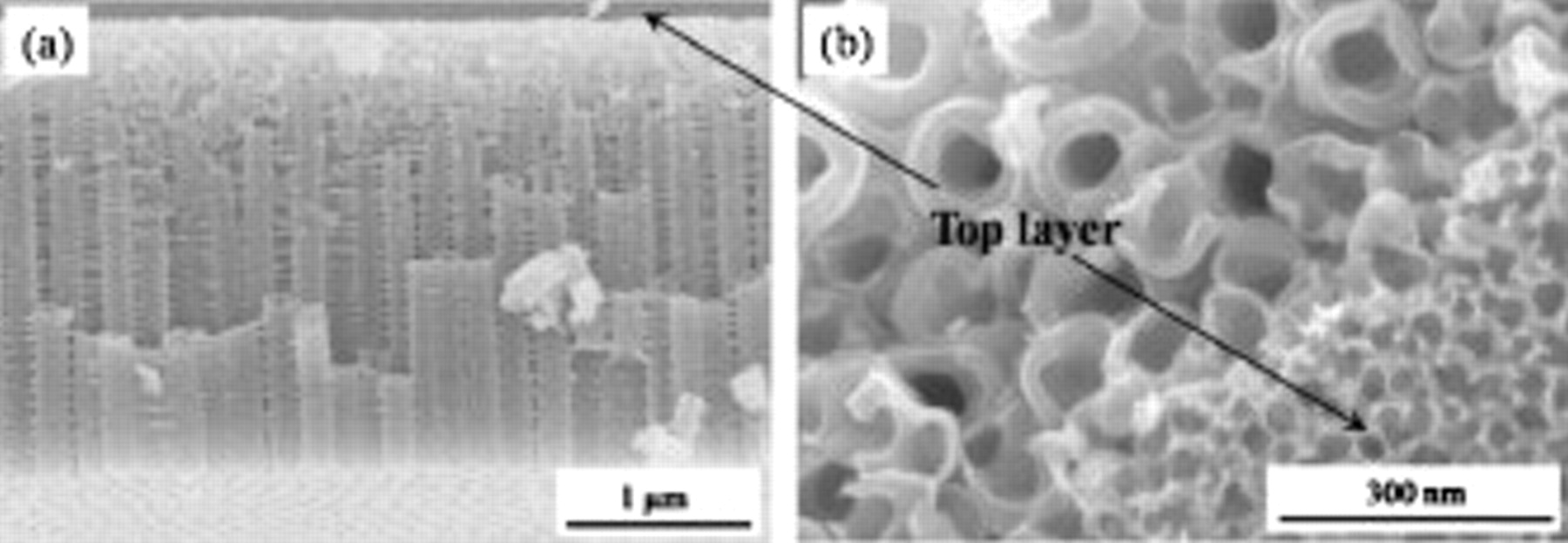
Figure 1. (a) A cross-sectional SEM image of ordered oxide nanotube layers grown on TiW alloy by anodization in a solution of EG with 0.2 M HF at 80 V for 1 h. (b) A top view of the interface between top porous and underneath nanotube layer.
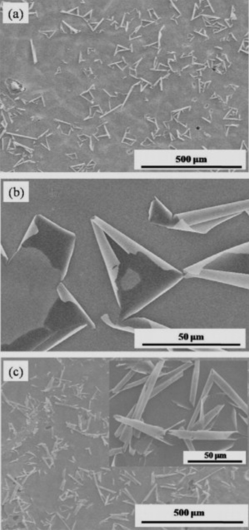
Figure 2. Surface morphology of  nanotube grown at 160 V for 30 min (a) with and (c) without water cleaning afterwards. (b) Enlarged view of surface image shown in Fig. 2a. The inset of (c) shows a magnified image.
More of the nature of the nanosheets becomes apparent by a closer examination of the layer. Figure 3a shows a magnified image of the nanosheet, which was rolled from the left side (indicated by an arrow). A typical porous layer structure like the images in Fig. 1b is observed on the right side in Fig. 3b, while on the left side (see also Fig. 3c), from which the nanosheet was peeled off, a highly ordered nanotube structure becomes opened up. On the bottom side of the nanosheet, shown in Fig. 3d, the regular tubular geometry (100 nm in diameter with a wall thickness of 25 nm) is already clearly imprinted.
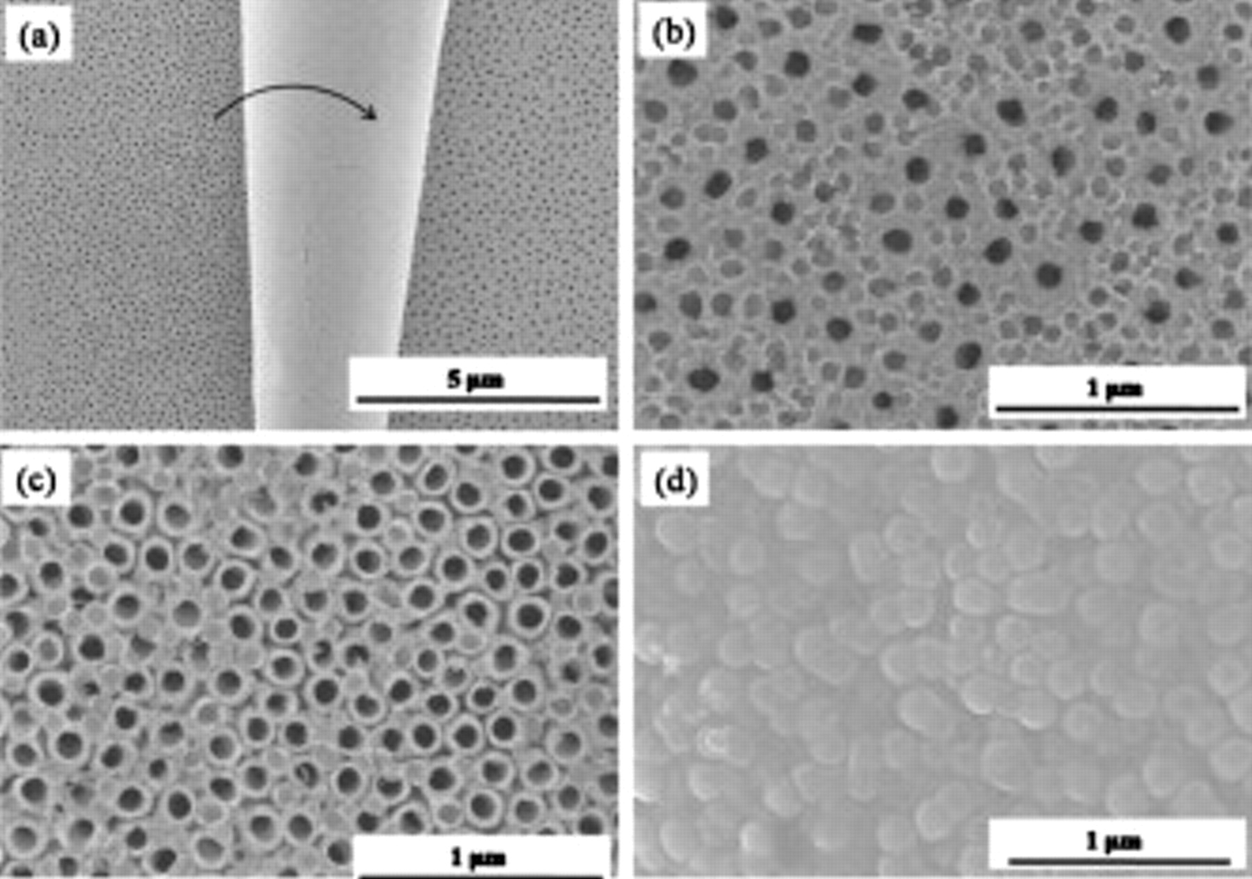
Figure 3. (a) SEM images of a peeled-off porous layer of  nanotube. [(b) and (c)] The magnified surface image of (a) at different places. (d) The bottom image of the porous layer in (a).
For practical use, the nanosheets which were formed by high potential anodization are successfully removed by a careful ultrasonic treatment. Figure 4 shows the top-view SEM images of the  nanotube layer after an ultrasonic agitation in DI water for 2 min. Apparently, a wide range of smooth surface is obtained compared to the samples before treatment (see Fig. 2a), which means that the nanosheet is successfully removed by the ultrasonic treatment. The magnified SEM image in Fig. 4b reveals that an open-top morphology of the nanotubes is present. The inner and outer tube diameter is almost the same as for the initiation-layer-free samples before the ultrasonic treatment. This implies that only the nanosheet is successfully removed without the breakage of the nanotube layer along their original length. Otherwise, a smaller inner tube diameter would be observed due to the thickening of the inner shell toward the tube bottom.23
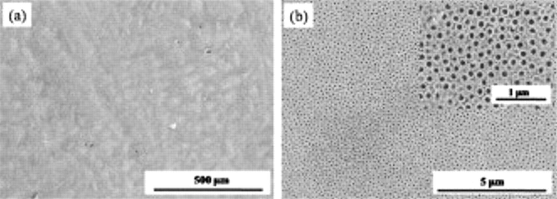
Figure 4. (a) The top-view image of self-organized  nanotubes layers after cleaning with water followed by ultrasonic treatment and (b) its magnified image.
Most likely, purely chemical reasons for the top layer delamination can be excluded in our study, as there is no distinctive difference in the composition between the porous and tubular layers which is confirmed by X-ray photoelectron spectroscopy (XPS) (for surface composition) and energy-dispersive X-ray analysis (for bulk composition) as shown in Fig. 5.
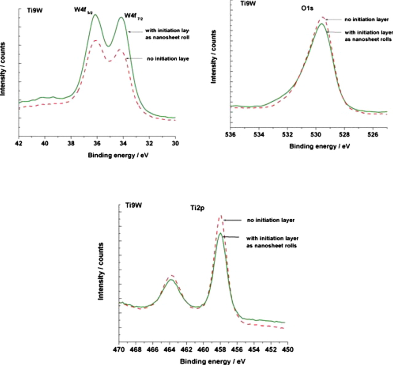
Figure 5. XPS spectra of W 4f, O 1s, and Ti 2p peaks for Ti9W with and without initiation layer as nanosheets scrolls.
To investigate some potential causes for the nanosheet delamination, the temperature of the Cu backplate connected to TiW substrate was monitored during the anodization process. This method provides a facile way to estimate the temperature profile even though the recorded temperatures are not the same as on the tube surface because the thermal conductivity of the oxide samples is not high. Figure 6a displays the temperature profile of TiW substrate measured during the anodization process at different potentials for 1 h. At 80 V, the temperature slightly decreases after anodization, while it increases and keeps steady in 120 V. In both cases, the temperature difference between the initial and the final process is only about  . However, a further increase in potential shows a drastic increase in the temperature. The temperature differences are found to be 8 and
  at 160 and 180 V, respectively. These temperature profiles at different potentials are highly related with current during the anodization process. Up to 120 V of potential, the current density does not change considerably, while at a potential higher than 160 V, the current density increases continuously from an initial stage to the end of anodization. Owing to the high current through the samples induced by a high anodization potential, local heating is generated during the anodization. In the nanotube structures of
  , porous layers could be relatively loosely connected to the underneath nanotube layers. Therefore, it is suggested that when a high voltage is applied to the sample, thermal stress due to the heating is produced, which results in a breakup at the oxide structure between the porous initiation layer and nanotube tops. While other break-away reasons (such as piezoelectric effects) may not be entirely excluded, on pure
  nanotubes similar effects could not be observed.
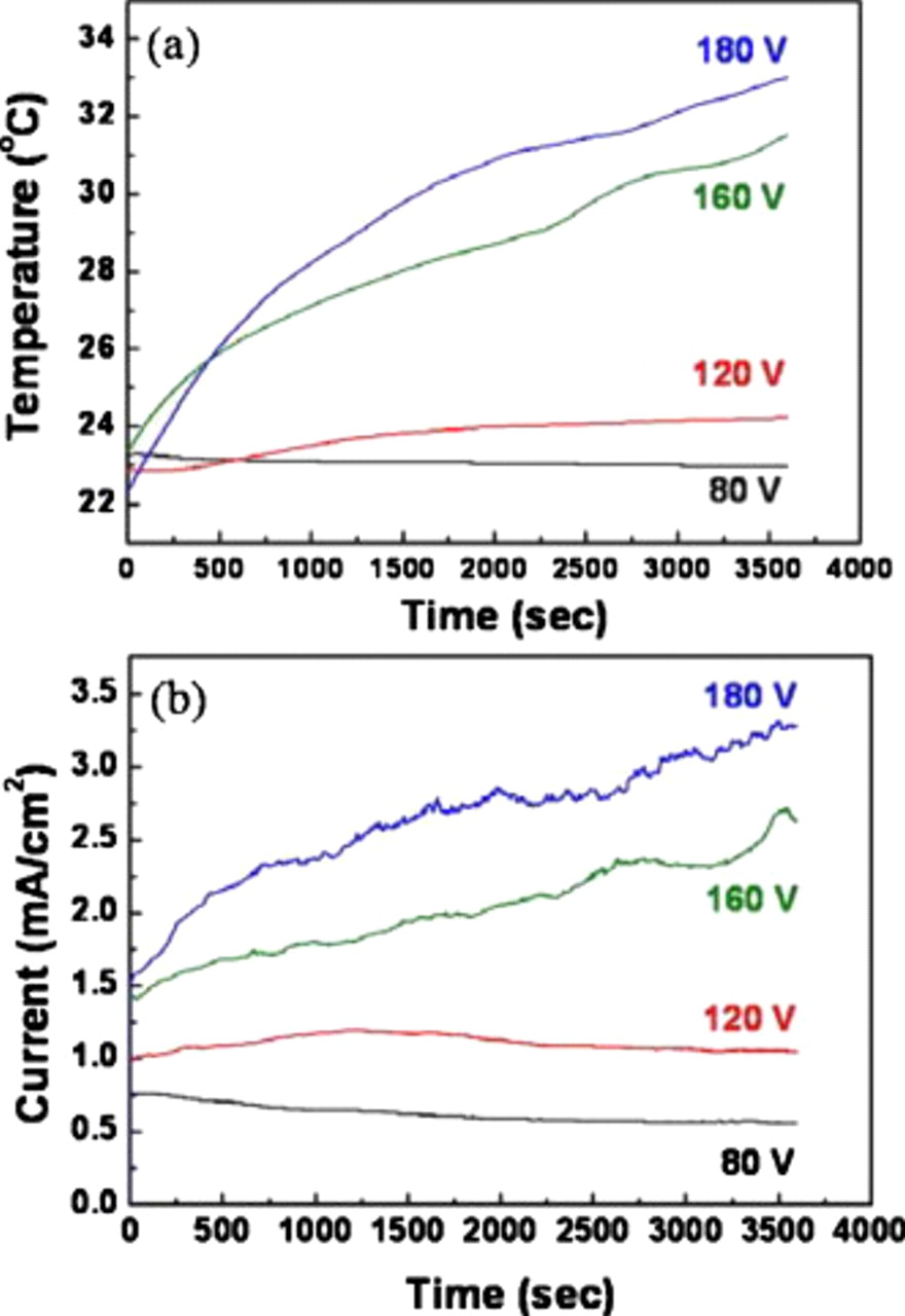
Figure 6. (a) Temperature profiles of TiW substrates monitored during the anodization in EG with 0.2 M HF for 1 h at different potentials. (b) The current transient recorded during anodization process.
Conclusions
In summary, a self-peeling of porous layer on top in the  nanotube was observed during the high potential anodization process, which is attributed to the breakup of the porous layer from the layer due to thermal stress. This self-peeled nanosheet was effectively removed after ultrasonic treatment into DI water. In this way, the open-top morphology of the
  nanotube structure was successfully obtained by high voltage anodization followed by ultrasonification treatment. The removal of a nonhomogeneous morphology on the top surface in the self-organized nanotubes has been an emerging issue because it significantly affects charge transfer which determines the overall efficiency in photovoltaic cells.22, 24 Several techniques have been proposed to avoid the irregular morphology of nanotubes.25–27 Our approach to eliminate the nonhomogeneous porous layer provides a very simple technique to fabricate a highly ordered open-top nanotube structure.
Acknowledgment
This work was supported by DFG and FP-6 (Ti-nanotubes). N.K.S. was supported by the Alexander von Humboldt Foundation. We also greatly acknowledge Cluster of Excellence-Catalysis, Engineering of Advanced Materials (EAM) in Erlangen. Dr. M. Oehring at GKSS Forschungszentrum in Geesthacht is acknowledged for providing the Ti–W alloys.
University of Erlangen assisted in meeting the publication costs of this article.