Abstract
In this work, we report some preliminary results concerning the fabrication of quaternary copper, indium, gallium, and selenium (CIGS) nanowires that were grown inside the channels of an anodic alumina membrane by one-step potentiostatic deposition at different applied potentials and room temperature. A tunable nanowire composition was achieved through a manipulation of the applied potential and electrolyte composition. X-ray diffraction analysis showed that nanowires, whose chemical composition was determined by energy-dispersive spectroscopy analysis, were amorphous. A composition of  , very close to the stoichiometric value, was obtained. These nanostructures were also characterized by photoelectrochemical measurements: They showed a cathodic photocurrent and an optical gap of 1.55 eV.
Export citation and abstract BibTeX RIS
Copper indium gallium selenide (CIGS) compounds are considered among the most efficient absorber materials for solar cell applications because they show relevant advantages, such as high absorption coefficients of visible light (up to about  ), ability to undergo bandgap engineering through alloy formation, and long-term optoelectronic stability.1, 2 For these features, CIGS-based solar cells compete with poly Si-based ones, and considerable efforts have been made to developing innovative devices using these materials. The excellent performance of CIGS compounds was attributed to a hole potential barrier at grain boundaries preventing electron–hole recombination. Despite this, the region could contain many defects.3 According to Yan et al. ,4 the superior performance of CIGS should not be explained exclusively in terms of grain-boundary behavior: They also attributed a key role to the existence of nano p–n junction networks in the entire CIGS film because of the formation of Cu-poor and Cu-rich nanodomains that exhibit n- and p-type conductivities, respectively.5 To date, the best performance was obtained by the NREL group: For a single-junction CIGS solar cell (laboratory scale device; area:
  ), a conversion efficiency of more than 20% was achieved.6 This device was fabricated by a process difficult to scale up because it is based on successive deposition steps; in particular, the CIGS absorber film was produced by a three-stage coevaporation process that can severely hinder the diffusion of this device.
Conversely, to make CIGS-based solar cells more attractive and competitive, low cost and easy scalability processes must be developed. In this context, electrodeposition can play a key role because it is a very simple and quick technique for obtaining good quality, large-area CIGS films compared with other fabrication methods.7, 8 A further advantage of the electrochemical route is the possibility to form homojunctions of CIGS without changing the electrolyte solution, as shown by Dharmadasa et al. ,9 who also evidenced how it is possible to simultaneously control a type of electrical conduction and energy gap (from 1.1 to 2.2 eV) by changing the applied voltage.
The overall reaction leading to the deposition of stoichiometric CIGS is

The exact mechanism is not well established because it depends on the redox potential of each species, solution composition, and applied potential.10 The most common hypothesis envisages the formation of different copper–selenium phases, followed by an incorporation of indium and gallium,7, 8, 11, 12 but according to the mechanism proposed by Kröger,13 the formation of 
 phases must also be considered because the deposition of selenium compounds occurs at potentials more positive than the deposition potential of less noble elements


These compounds can either chemically or electrochemically react with each other, leading to the formation of ternary and quaternary compounds


To our knowledge, up to now, simultaneous electrodeposition of Cu, Ga, In, and Se was investigated only for the fabrication of thin films, while in this work the extension to the fabrication of nanowires (NWs) is proposed. Only ternary chalcopyrite (CIS) NWs have been prepared by Phok et al. ,14 who proposed a pulsed cathodic electrodeposition. A great difficulty in synthesizing quaternary chalcopyrite through an electrochemical route is related to the codeposition of Ga because its standard electrochemical potential is very low in comparison with those of the other elements.15 In a recent paper, Fu et al.16 suggested that  concentration in the electrolyte solution is a key parameter controlling the electrochemical growth of CIGS. In the electrodeposition into the anodic alumina membrane (AAM) nanochannels, the control of the electrolyte composition is more challenging because mass transport in a confined ambient occurs at a different rate than in bulk solution. Despite this difficulty, synthesizing nanostructured quaternary chalcopyrites are of great technological interest because of their enhanced performance. In fact, photovoltaic devices employing semiconductor NWs display high values of energy conversion efficiency compared to conventional thin-film devices.17–20 Aligned NWs with a controllable composition modulation can give ordered p–n junctions and continuous charge carrier transport pathways without recombination.21 Therefore, NW solar cells might provide an even higher efficiency, as shown by Law et al.22 To increase electron diffusion length in a dye-sensitized solar cell, these authors replaced the nanoparticle film with an array of oriented single-crystalline NWs. Because of the very large surface area of this device, a better absorption of red light and a very efficient carrier collection were achieved. Kamat showed that solar devices consisting of nanorod arrays display superior performances with respect to planar junctions.23 In fact, when semiconductor nanorods, presenting p–n junctions along the radial direction, are arranged in a vertically aligned array, light can be absorbed along the rod length and charge carriers diffuse radially for a shorter distance toward the junction.17, 23
In this work, we successfully used the electrochemical route for fabricating, in one step, regular arrays of CIGS NWs by template electrodeposition24–27 from an unbuffered sulfate-based electrolyte. Photoresponse and type of conduction of the NWs are also investigated.
Experimental
CIGS NWs were electrodeposited potentiostatically into AAMs at room temperature for 1 h from a nitrogen-purged aqueous solution containing  ,
,  ,
,  , and
, and  . Experimental procedures for deposition within AAM pores of nanostructures were detailed in our previous works.25–27 Briefly, before electrochemical deposition, a layer of Au films (about 150 nm thick) was sputtered onto one surface of the AAM; then, the template was mounted onto an aluminum support by a conductive paste, and the active surface (about
  ) was delimited by an insulating lacquer.
To optimize the stoichiometry of the final deposit, electrochemical baths with different compositions were tested. Electrolytes were obtained mixing different volumes of solutions of  (0.2 mM),
  (0.4 mM),
  (0.8 mM), and
  (0.4 mM), all prepared using deionized water. The solutions were prepared under vigorous stirring, and the final pH, without any adjustment, ranged from 1.6 to 2.6. Electrodeposition was performed at a constant applied potential varying from −0.605 to −1.05 V/normal hydrogen electrode (NHE). Electrochemical experiments were performed using a PAR potentiostat/galvanostat (model PARSTAT 2273). A standard three-electrode cell was employed, with a graphite sheet and a saturated calomel electrode as counter and reference electrodes, respectively. The chemical composition and structure of CIGS NWs were investigated by energy-dispersive spectroscopy (EDS) and X-ray diffraction (XRD). These characterization methods are described in detail elsewhere.25–27 Morphological analyses were performed by scanning electrode microscopy (SEM) using an FEI field-emission gun (FEG) environmental scanning electron microscope (model QUANTA 200) equipped with EDS.
Photoelectrochemical measurements were carried out at room temperature in an aerated 0.1 M  solution using a three-electrode cell. A Pt net served as the counter electrode, and the reference was a standard mercury sulfate electrode. The cell was equipped with flat quartz windows for allowing sample illumination, obtained using a 150 W Xe lamp (Oriel) coupled to a UV/visible monochromator (Baush & Lomb), mounted in an optical line with quartz optics. Photocurrent was detected by a two-phase lock-in (EG&G, model 5206), connected to a mechanical chopper (frequency: 10 Hz). To suppress second harmonic responses, a yellow filter was inserted in the light path before recording photocurrents at long wavelengths. The schematic diagram of the experimental apparatus used for the photoelectrochemical investigations is shown in Fig. 1. Photocurrent spectra reported below were corrected for the photon emission at each wavelength of the lamp/monochromator system; the latter was detected using a calibrated thermopile (Newport).
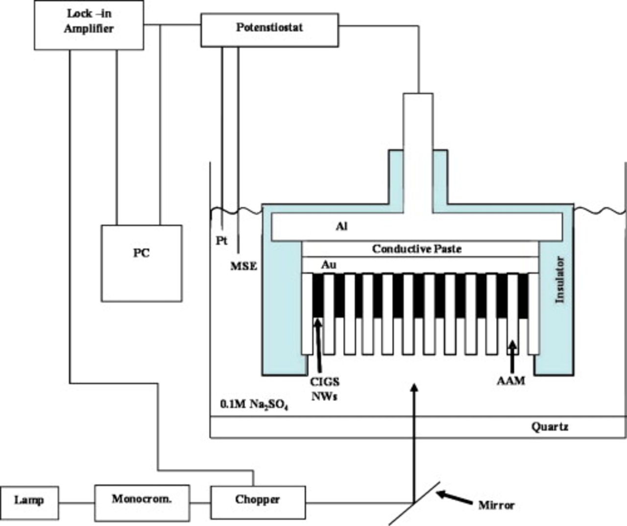
Figure 1. Scheme of the setup used for the photoelectrochemical experiments.
Results and Discussion
The number of different reactions that may take place for the simultaneous electrodeposition of Cu, In, Ga, and Se explains the difficulty of obtaining a stoichiometric deposit. In fact, the final composition depends on the applied potential compared with the redox potential of the single elements, on the overvoltage for charge transfer, on the concentration of ions in solutions, and on the substrate used. To obtain CIGS with a composition as close as possible to the stoichiometric one, we have investigated the deposition process in a potential range (from −0.605 to −1.05 V/NHE) more negative than the redox potential of  . It has also been necessary to optimize the composition of the electrolyte solution by adjusting the
  molar ratio from 0.8. to 2.4 to deposit the amount of Ga fulfilling the required stoichiometry. The systematic investigation of the deposition process and the analysis of the polarization curves will be presented and discussed in a future work. For the sake of brevity, we report only the results obtained at one applied potential and electrolyte concentration.
NW composition was evaluated by a quantitative EDS analysis performed on the as-deposited sample. Figure 2a shows a typical EDS spectrum revealing the presence of peaks of Al, O, and P, arising from the alumina template, in addition to peaks of Cu, In, Ga, and Se. Au peaks come from the gold film sputtered on the back side of the alumina membrane before electrodeposition.25–27 The composition of CIGS best approaching the stoichiometric value was obtained at −0.905 V/NHE from a bath having a  molar ratio of 2.4, and it is reported in the table of Fig. 2a, where the ideal stoichiometry of the CIGS compound is also shown for comparison. The as-deposited CIGS NWs have an amorphous structure, independent of applied potential and electrolyte composition, as shown by the XRD analysis of Fig. 2b: Only peaks due to the gold layer are present, while the broad band around 30° is characteristic of amorphous alumina. The amorphous structure was expected on the basis of the literature.8 An interesting result of the XRD analysis is the absence of any peak attributable to the metallic phases of four elements. This finding supports the conclusion that the four electrodeposited elements are totally mixed in a single amorphous phase. Further investigations are in progress to evidence the effect of thermal treatment on the structural and chemical features of the deposit and to elucidate possible modifications of its behavior under illumination.
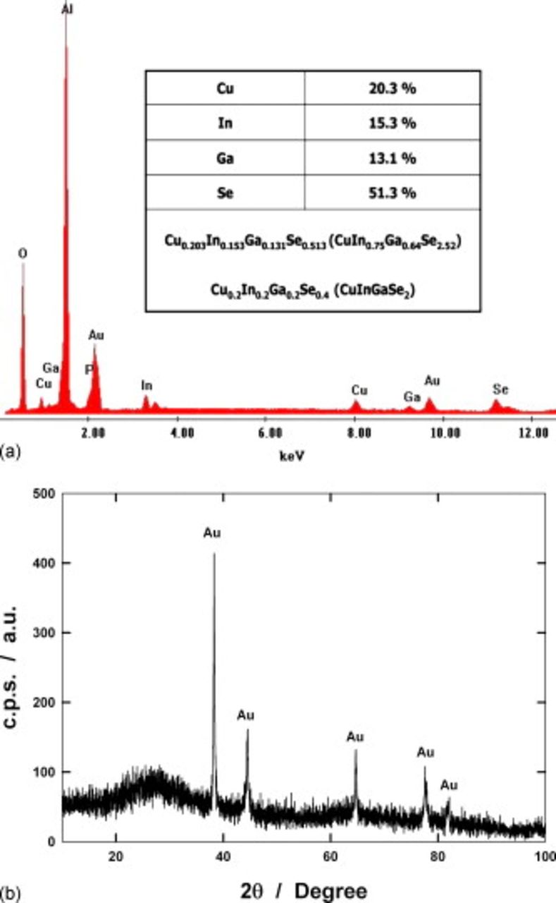
Figure 2. (a) EDS spectrum of as-deposited CIGS NWs. In the inset, composition of the wires is reported. For comparison, the ideal stoichiometry of CIGS compound is also reported. (b) XRD patterns of NW filled membrane. Electrodeposition was conducted at −0.905 V/NHE with a  molar ratio of 2.4.
In all deposition conditions, the morphology of CIGS NWs was similar to that shown in the FEG-SEM images in Fig. 3: The presence of some broken NWs is due to sample preparation before FEG-SEM analysis. In particular, Fig. 3a shows that NWs are uniformly distributed in all channels of the membrane, and their population density is of the order of  , equal to the pore population of the AAM template. To better evidence the morphology of the wires, FEG-SEM analysis was also performed after the complete dissolution of the membrane in 2 M
  aqueous solution. Some of these micrographs were reported in Fig. 3: Fig. 3b shows that NWs are straight with a cylindrical shape; their uniform diameter (about 210 nm) is almost equal to the size of the AAM channels, and the mean length is
  . Figure 3c and 3d displays, respectively, the secondary electron (SE) and backscattered electron (BSE) images of the NW array: They reveal that NWs consist of a homogeneous phase.
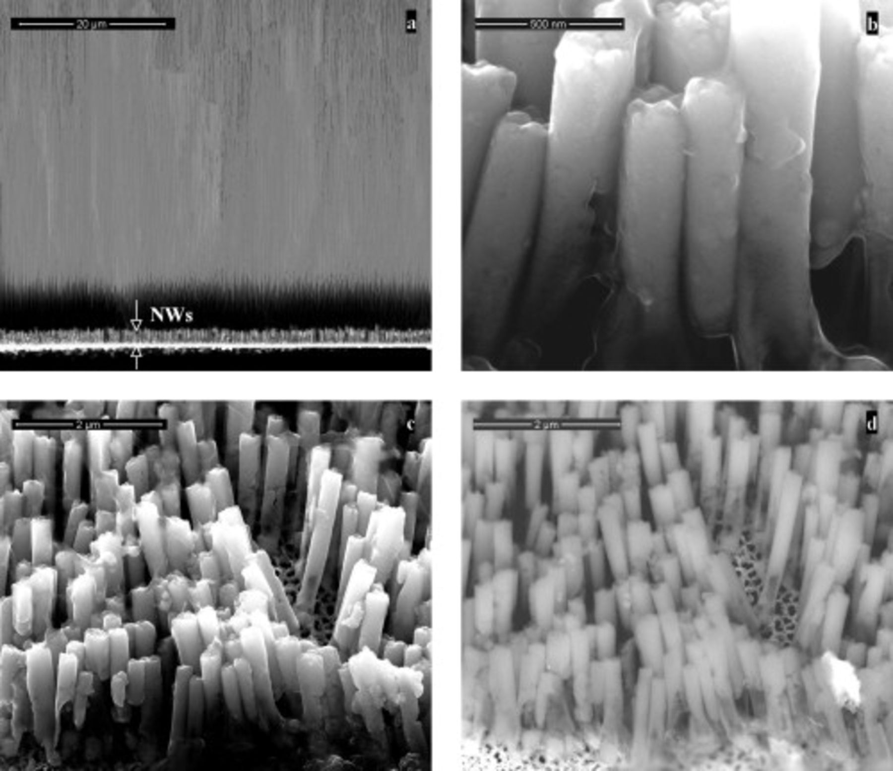
Figure 3. FEG-SEM images of the CIGS NWs of Fig. 2. Cross-sectional view of NWs (a) before and (b) after total dissolution of the AAM template. (c) SE and (d) BSE images of the CIGS array after template dissolution.
CIGS NWs are photoactive, as revealed by a photocurrent analysis carried out in 0.1 M  aqueous solution, using the setup shown in Fig. 1. Figure 4 shows the photocurrent action spectrum, corrected for the lamp photon emission, for the NW array of Fig. 3 recorded at −0.05 V/NHE, slightly negative with respect to the open-circuit potential (0.0 V/NHE): Two photocurrent peaks are present in the spectra, at around 450 and 560 nm, whose relative intensity changes with experimental conditions. Both from the photocurrent onset wavelength and from the
  vs
vs  plots, an optical gap close to 1.55 eV has been estimated within the interval reported for crystalline films.8, 9 Photocurrent is cathodic, as revealed by the current transients obtained by manually chopping light under continuous illumination with different wavelengths (insets in Fig. 4). These last experiments showed the presence of photocurrent spikes having the same sign of the pseudostationary response. The p-type conductivity observed here suggests that NW composition must be controlled to obtain n-type CIGS according to the results reported in Ref. 9. For this scope, the electrochemical technique can be useful because chemical composition can be controlled by adjusting the applied potential.9 However, in the electrodeposition in a confined ambient, ion transport within membrane channels can play a key role at variance of thin-film deposition.
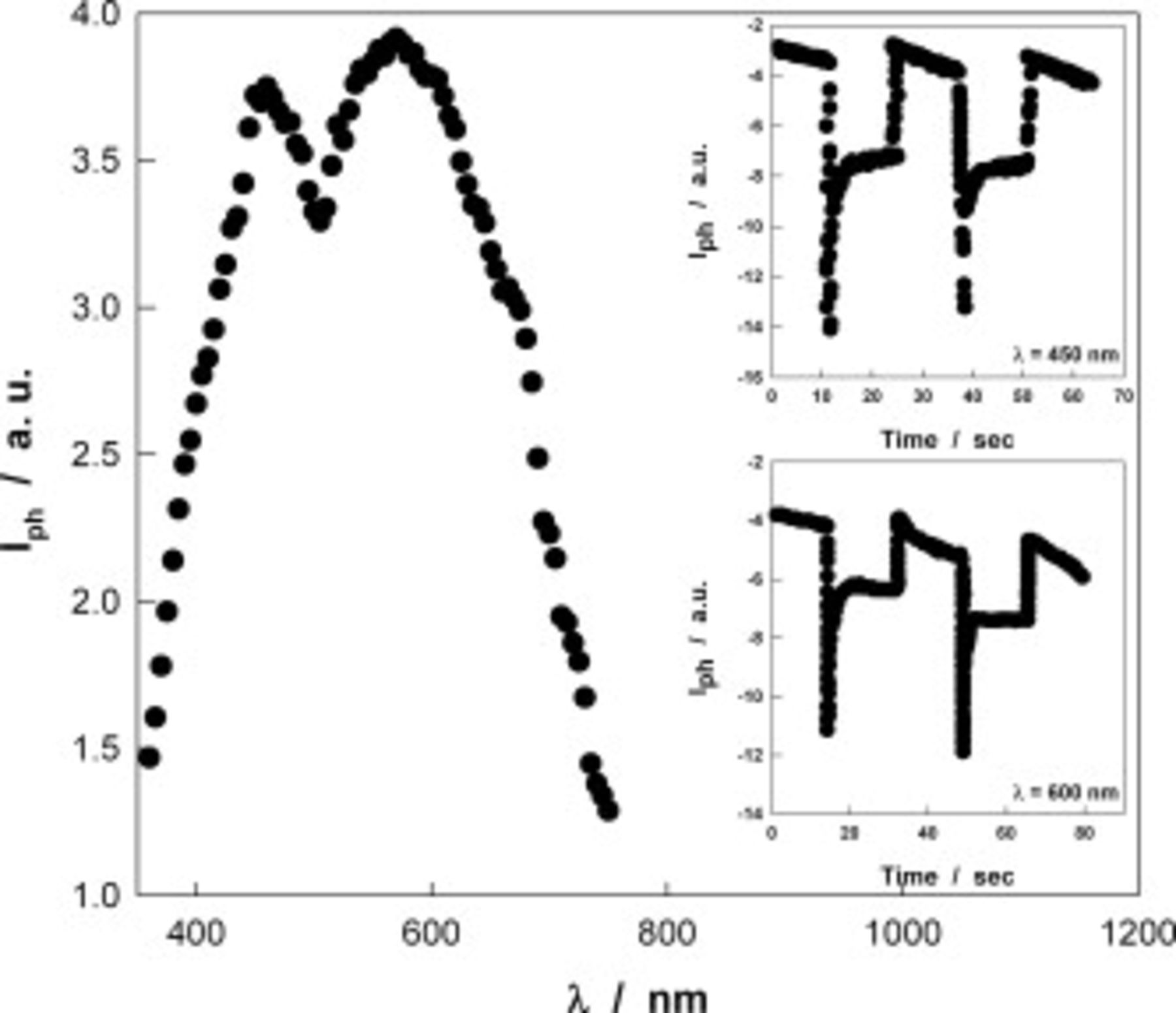
Figure 4. Photocurrent spectrum of the NW array of Fig. 2. Insets: Current transients under monochromatic irradiation at 450 and 600 nm.
Conclusions
In summary, we have obtained amorphous CIGS NWs by one-step electrochemical deposition into AAMs. A stoichiometry of  was obtained at −0.905 V/NHE from a bath with a
  molar ratio of 2.4. SEM analysis showed that all channels were filled with perfectly cylindrical wires; thus, NW population was equal to the pore surface density of the AAM template. NWs display a cathodic photocurrent and an optical gap of about 1.55 eV.
These preliminary results are very interesting because after heat-treatments it is possible to obtain different compositions (due to the high selenium volatility) and crystalline structures, which should improve the photocurrent performance of these materials. Further studies are in progress to investigate these issues.
Acknowledgments
This work was financially supported by Università di Palermo.
Università di Palermo assisted in meeting the publication costs of this article.