
Abstract
A copper-to-copper bonding process was developed for an all-copper, chip-to-substrate interconnect technology. High aspect ratio polymer molds for electroplating were formed using a photodefinable polymer on both the chip and the substrate surfaces. Copper pillars were fabricated by electroplating metal in the polymer molds. The chip-to-substrate all-copper connections were formed by joining the two pillars with electroless copper plating followed by an anneal process. The copper-to-copper bonding of the high aspect ratio pillars does not require the use of solder or other noncopper metals. Mechanical shear force measurements were used to characterize the bonding process as a function of annealing conditions. Excellent bond strength of the electrolessly joined pillars was achieved with a  anneal, with the bond strength of the copper pillar interconnects exceeding
  . High aspect ratio pillars can provide mechanical compliance, and the electroless fabrication method compensates for pillar misalignment and nonplanarity of the bonded surfaces.
Export citation and abstract BibTeX RIS
Solder is widely used in the electronics industry for attaching components to substrates or printed circuit boards in a flip-chip configuration. The melting point of solder, and its ability to adjust to lateral (self-alignment) and vertical (nonplanar) surfaces, make it valuable in ball-grid array (BGA) packages and epoxy substrates. However, solder has modest electrical properties and copper-tin intermetallics have poor mechanical properties. The electromigration resistance of solder materials is low. The International Technology Roadmap for Semiconductors (ITRS) projects that high-performance chips in 2007, 2008, and 2012 will require a supply current of 172, 198, and  , respectively.1 This will exceed the maximum allowable current density of solder,
  , given the projected number of power and ground input/output (I/O) interconnects.1 The solder connection is limited to an aspect ratio of roughly unity so that high profile (large chip-to-substrate stand-off distance) is very difficult to fabricate. High aspect ratio and nonspherical connections are needed for high I/O density and mechanical compliance for IC-to-substrate connections. Very high frequency signal I/O, up to
  , are projected for future microprocessors.1 Many solders have poor mechanical strength.2 For example, tin and other solder-containing metals form brittle intermetallics with copper, which can fracture under high shear and normal stresses. Underfill is required between the chip and substrate to support the solder connections. The underfill distributes the thermomechanical stresses originating from the coefficient of thermal expansion (CTE) mismatch between the different materials.3 Organic substrates are most often CTE-matched to copper
  so that flat boards can be fabricated, however silicon has a CTE of about
  .
.
An all-copper connection technology between the copper wiring on the integrated circuit (IC) to the copper wiring on the substrate would provide high conductivity electrical connections, excellent resistance to electromigration, and avoid the formation of brittle intermetallics.4 Further, if the copper connections had a high aspect ratio, then mechanical compliance could be designed into the connections so that no underfill would be needed. The elimination of underfill would improve the electrical environment (lower permittivity and loss) and potentially lower the cost because one less material and process step is required.
Copper wafer bonding (copper-to-copper fusion) can be used to produce all-copper connections. The critical parameters of copper-to-copper bonding involve  the method of achieving intimate contact between the two clean, pure-copper surfaces, and
  the bonding temperature, pressure, and cleaning conditions. In order to obtain adequate bonding between two copper surfaces, high-temperature annealing
  of "clean" copper surfaces under pressure is required.5, 6 The higher end of the temperature range is preferred to create seamless copper joining. However, this temperature range is too high for cost-effective organic boards or substrates. An upper temperature of
  is required for epoxy or BT boards to avoid board degradation. If the copper wafer bonding process were used for I/O, there would also have to be excellent alignment between the two parts so that the contact area between the top pads being joined is as large as the pad area because the copper does not flow and readjust, like solder does. Finally, direct copper-to-copper wafer bonding requires either flat surfaces or surfaces that can withstand high pressure to make them flat during bonding because there is no mechanism to account for vertical height variations. Surface activated bonding (SAB) has been shown to provide a route for room-temperature copper-copper bonding with the reported bonding strength above
  .7 This room-temperature bonding process was achieved by bonding two extremely flat and clean copper surfaces under an ultrahigh-vacuum environment.7 Similar to copper wafer bonding, it has little tolerance for spatial misalignment. Solder can be easily distorted during reflow to elongate or flatten, as needed. A practical interconnect structure currently used has a reflowable solder cap on the copper pillar.8 Wang et al. used high aspect ratio copper pillars to improve the I/O density.8 The solder cap avoided the high-temperature copper-to-copper bonding problem. However, the electrical and mechanical limitations of solder still exist.
In this work, an electroless copper plating and annealing process has been developed to fabricate all-copper chip-to-substrate connections. The pillars are fabricated and electrolessly joined at ambient temperature. It is most desirable to have the anneal temperature be compatible with epoxy boards (i.e.,  ). The atomic mixing of the copper pillars during the plating process allowed the reduction in annealing temperature. The mechanical compliance of the all-copper interconnects was determined by the aspect ratio of the electroplated pillars.
Experimental
The fabrication process is shown in Fig. 1. A seed layer of 
 was first dc sputtered on the bare silicon wafer. Additional samples were fabricated with Cr in place of the Ti to improve the wafer adhesion. A
  layer of silicon dioxide was then deposited on top of the titanium surface by plasma enhanced chemical vapor deposition (PECVD) at
  . Microposit SC1813 photoresist (Shipley Corporation) was spun on the silicon dioxide surface. After photopatterning the photoresist layer, buffered oxide etch (BOE) was used to etch the
  and Ti layers in the exposed areas. The remaining photoresist was removed in an acetone rinse. Next, a thick layer of Avatrel 2195P polymer (Promerus LLC, Brecksville, OH) was spun on top of the patterned
  layer. The spin rate of the polymer was
  for
for  followed by
  for
for  . After
  softbake on a hot plate at
  , a
, a  UV exposure dose was performed (
 irradiation). A
  post exposure bake at
  was used followed by ultrasonic developing to produce high aspect ratio, hollow-core polymer plating molds.
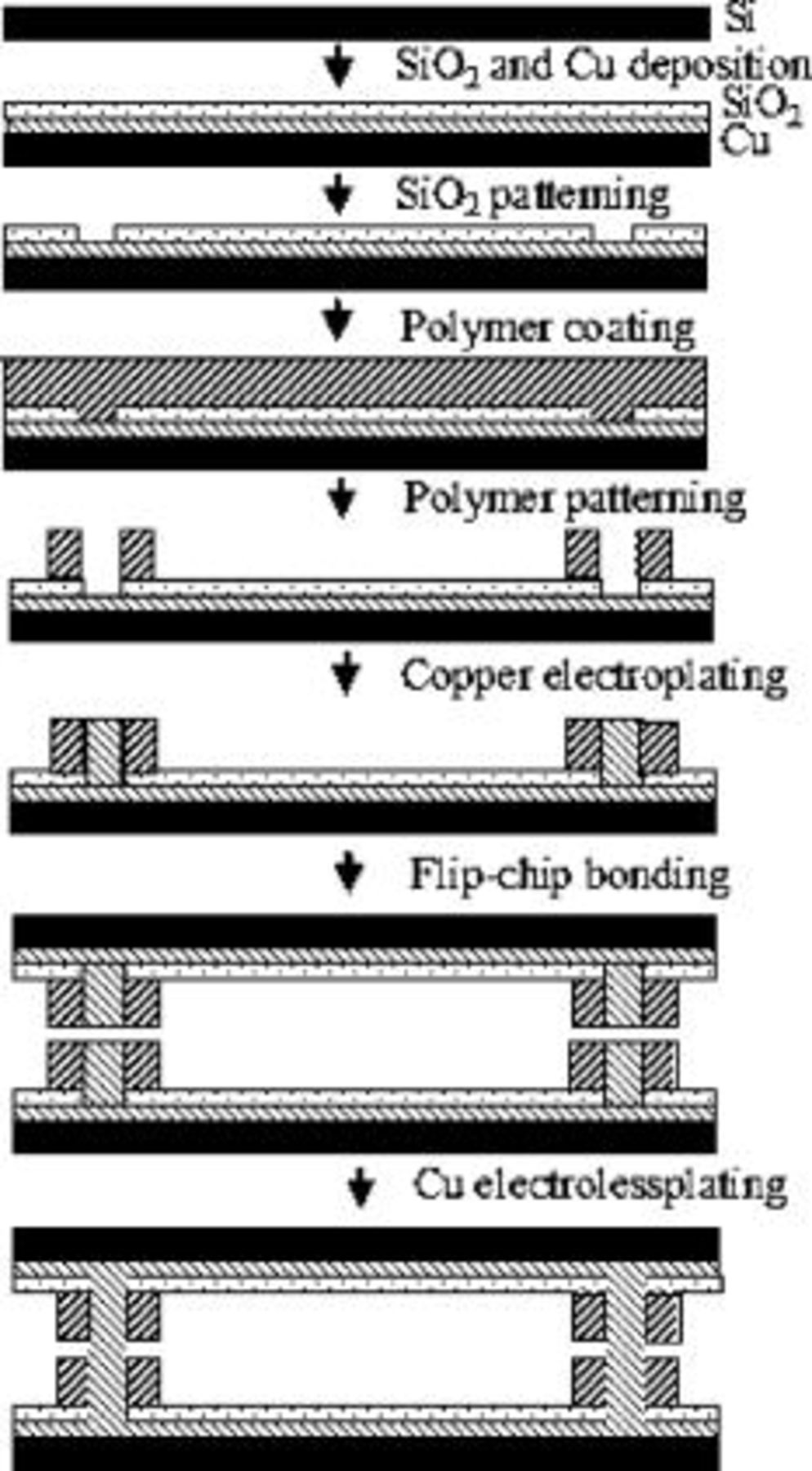
Figure 1. Fabrication process flow.
Copper electroplating was then used to fill the polymer cavities and produce copper pillars. The plating solution contained 
 ,
, 
 ,
,  brightener, and
  carrier. Electroplating was performed at
  constant current for
  . Two pillar-containing chips were aligned using a flip chip bonder and held in place using wax. The wax was used to temporarily hold the bonded chips and was removed during the copper annealing step. The two pillars were joined using electroless copper plating. A copper sulfate, ethylenediaminetetra acetic acid, formaldehyde electroless bath at
  was used for
  to join the two parts and plate a fillet of copper in the void between the two pillars. After the two copper pillars were electrolessly plated together, they were annealed at various temperatures in a nitrogen environment.
Results and Discussion
The three critical aspects of this fabrication process are  the creation of the high aspect ratio copper pillars using photodefined polymer molds,
  joining of the two copper pillars and bridging the gap between the pillars by electroless plating, and
  annealing and recrystallizing the newly formed joint between the pillars so as to provide adequate mechanical strength.
The photosensitive polymer used in the fabrication must be capable of producing high aspect ratio structures with vertical sidewalls because of the need for tall, compliant IC-to-substrate copper connections. The plating mold must also be tolerant to long exposures to the plating bath. The pH of the electroplating bath and the electroless plating bath are 1.5 and 12.5, respectively. Avatrel 2195P was used as the plating mold because it easily forms high aspect ratio structures and has excellent stability in the plating solutions.9 Although high aspect ratio plating molds could be fabricated (aspect ratios  , height:width), an aspect ratio of 2:1 was used for the plating mold on each of the two pillars to be joined for test purposes here. Additional studies with high aspect ratio pillars will be reported in a later article.
Electroless copper plating was used to join the two copper pillars together. As the two pillars, in near-contact, were electrolessly plated with copper, the surfaces of the two pillars merged together and formed a metal-metal joint. After plating, the sample was annealed in a nitrogen atmosphere to recrystallize the bonded joint. Figure 2 shows the joined copper pillars after a  ,
,  anneal and removal of the top substrate.
  was chosen because the Avatrel plating mold decomposed at that temperature leaving the exposed copper pillar. After annealing and decomposition of the Avatrel, the top substrate was sheared off so that the joint between the pillars could be examined. The electroless copper bonding material between the two pillars can readily be identified in Fig. 2 by its elongated horizontal dimension. The fracture of assembled copper pillars with electroless joining occurred at the copper-to-silicon dioxide interface. Figure 3 shows a top view of the surface with one pillar structure remaining on the surface (sheared from the second surface) and one site where the pillar is missing (remaining on the mated surface). In each case, the copper joining process was stronger than the pillar-to-substrate adhesion. No pillars were fractured at the center joint.
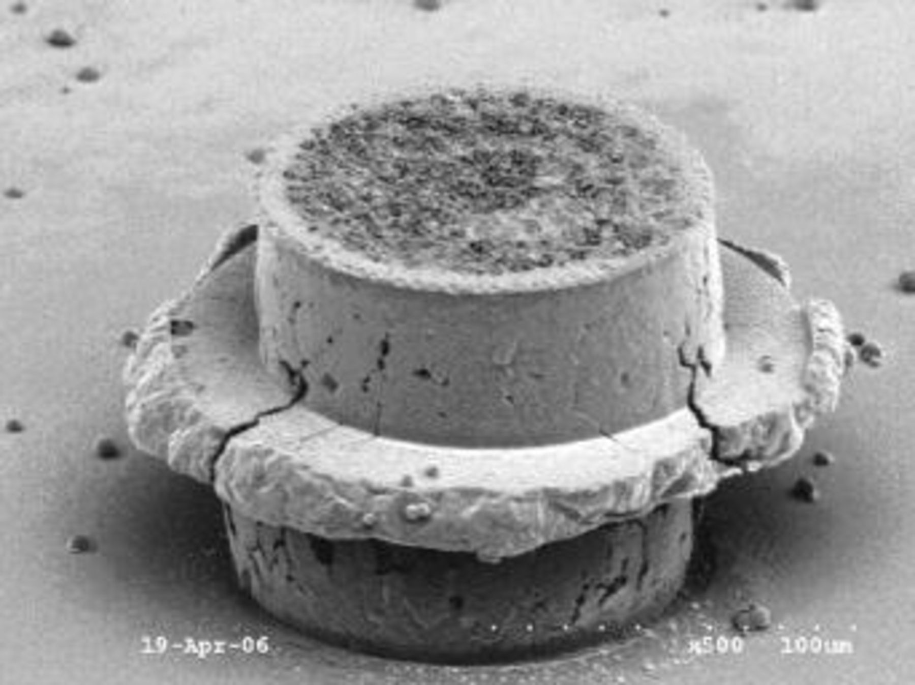
Figure 2. SEM picture of a joined copper pillar ( wide by
  tall).
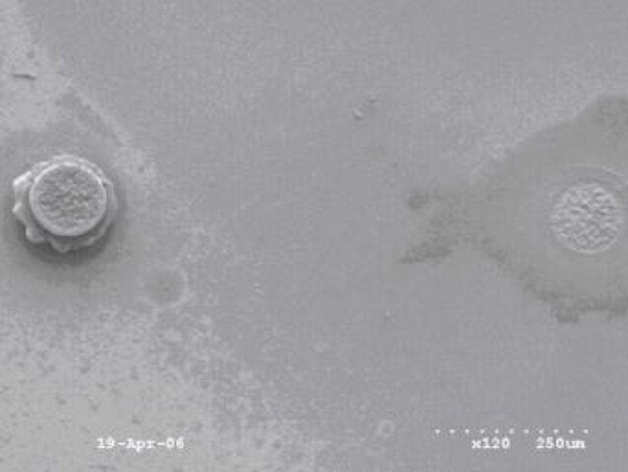
Figure 3. SEM picture of a sheared off substrate.
The electroless copper filled the opening between the two pillars and plated outward from the intersection of the pillars. A slight misalignment of the two pillars in Fig. 2 can be seen upon close inspection. However, the lateral (outward) plating of the electroless copper more than compensated for the spatial misalignment. The cross-sectional area of the joint between the pillars was greater than the area of the pillars so no loss of conductivity would be suffered. The seam between the electroplated copper pillars is dense with minor surface imperfections and cavities on the sidewalls, which are likely due to air entrapment during copper plating.
An important aspect of the electroless copper joining process is the ability to fill the gap between the two pillars. The pillars were cross-sectioned by grinding and polishing to examine the joint between the two surfaces. Figure 4a is a typical cross section showing two pillars (one from each surface) joined in the center (wide metal region) by the electroless copper. Some voids were observed in the center of the electroless metal as shown in Fig. 4b at a higher magnification. The small voids were restricted to a vertical height matching the height of the electroless plating region seen on the edge of the pillar structure. The number and size of voids in the electroless plated region varied for different samples. The conditions for electroless plating, distance between the two pillars, and annealing conditions affected the void structure. Control of the void region will be reported in a future manuscript.
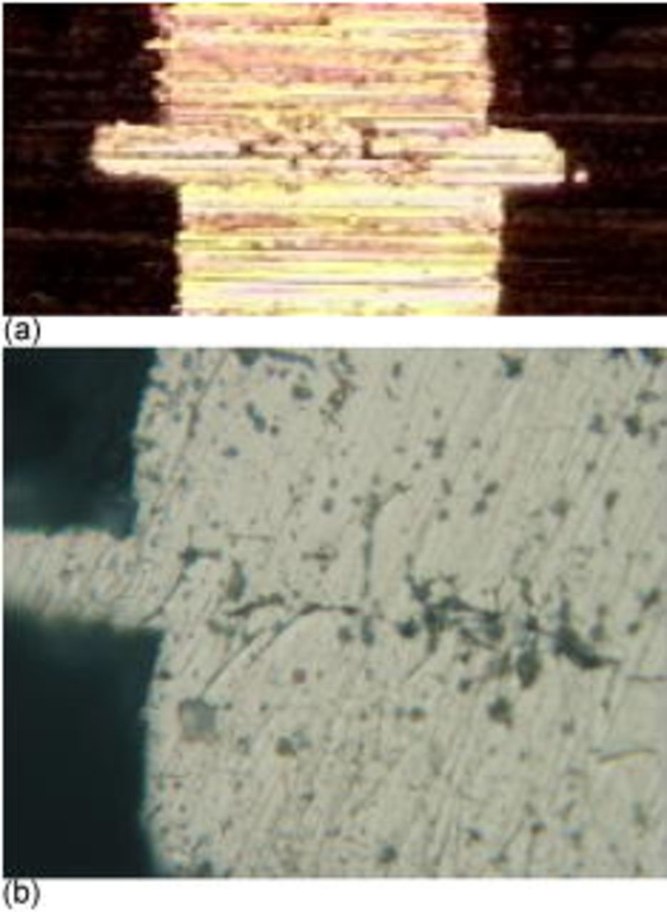
Figure 4. (Color online) Cross sections of bonded Cu pillars: (a) rough, and (b) polished.
The results show that the electroless plating process filled the offset between the two pillars. Each of the pillars examined was joined by the electroless process, although the gap varied from sample to sample. This ability to fill the void between near-mated pillars is an essential aspect of the chip-to-substrate connection. As a result, the two pillars did not have to touch at each location prior to electroless plating. Attempts were made to measure the contact resistance between the two electrolessly plated pillars. The resistance of the electroless copper region was less than the contact resistance to the pillar.
The bond strength of the joint is a very important part of the copper pillar attachment. The shear force for separating the two substrates was measured and reported in Table I. The sample annealed at  (entry A) was comprised of four copper pillars and sheared at a force of
  . Because the polymer plating mold had been decomposed (was absent), it did not contribute to the adhesion of the two parts. Based on the area of the four pillars (
 diameter), the shear stress, corresponding to the adhesion of the titanium to the silicon dioxide, was
  . The pillar-to-pillar electroless copper metal did not shear in any of the samples tested. To investigate the effect of anneal temperature, samples were annealed at different temperatures. Entry B shows the shear force for a set of four pillars plated and annealed at
  . The sample again fractured at the metal-to-silicon dioxide interface; however, the Avatrel was present and contact was achieved between the two sides. Thus, some of the
  force was due to the Avatrel. A second sample was prepared for
  annealing (entry C); however, Cr was the adhesion layer, rather than Ti, and the Avatrel did not bridge the two sides. The shear force was
  and the fracture occurred at the metal-to-silicon dioxide interface. The value is higher than entry A most likely because the Cr provided greater adhesion. The copper-to-copper joint did not rupture. Finally, a sample with a Ti adhesion layer was annealed at
  and resulted in a lower shear force, but the fracture occurred at the metal interface. Lower-temperature samples sheared at the copper-to-copper joint. The annealing temperature controls the copper grain size distribution, grain boundary character distribution, and crystallographic texture.9 It is most desirable to have the anneal temperature be as low as possible for semiconductor device purposes. A full study of the effect of annealing temperature is underway.
Table I. Maximum shear forces of bonded copper pillars with different anneal temperatures.
| Entry | Anneal temperature 
| Anneal duration (h) | Shear force | Adhesion layer |
|---|---|---|---|---|
| A | 400 | 1 | 1.404 | Ti |
| B | 250 | 1 | 4.840 | Ti |
| C | 250 | 1 | 1.800 | Cr |
Conclusion
A fabrication process was developed to obtain all-copper chip-to-substrate connections. Copper structures were first fabricated through electroplating in a polymer mold. A copper electroless plating step was used to join the copper structures. After annealing under nitrogen environment, the bonded chips were mechanically sheared, and the newly formed copper joint was stable, with bond strength greater than  . This fabrication process also shows the capability to compensate for misalignment and height variations of the bonded structures.
Acknowledgments
The authors acknowledge the collaboration of Patrick Thompson from Texas Instruments, Daniel Lu from Intel Corporation, and the support from the Semiconductor Research Corporation (SRC), 1341.001.
Georgia Institute of Technology assisted in meeting the publication costs of this article.