
Abstract
Continuous and modulated discharges, fed with divinyltetramethyldisiloxane mixed with oxygen and argon, were used to deposit carbon-doped silica-like (SiCOH) low- to ultralow-
 films. The effect of various process parameters on the dielectrical and thermal properties of films as well as on their chemical composition were investigated. As deposited, the SiCOH films exhibited dielectric constants from 4.45 to 2.70. Thermal annealing in the
  temperature range was found to be necessary to reach ultralow-permittivity values, but the temperature must be controlled in order to prevent an excessive collapse of the silicate matrix, which leads to poor thermal stability and mechanical properties. Lowering the oxygen content in the discharge allowed for a continuous decrease in
  values down to 2.32 when low radio frequency power was used, with a limited film thickness loss upon annealing of 11%. Fourier transform infrared spectra of ultralow-
 film exhibited intense absorptions from C-containing moieties, like
  and
and  . Upon annealing at
  , the organic content considerably decreases, though the loss of
  groups is quite limited. Thermogravimetric analysis coupled with mass spectrometry revealed that during thermal treatment, silicon-containing fragments were lost from the matrix along with hydrocarbon ones.
Export citation and abstract BibTeX RIS
Over the past few decades improvements in integrated circuit (IC) performances have been mainly achieved by reducing transistor sizes. This has enabled greater transistor speed and an increased number of transistors being implemented on the same chip. As a consequence, the intrinsic gate delay, which is the transistor switching time, decreases. However, the increased transistor density requires wiring density to increase as well, and for feature sizes smaller than  , the speed of signal propagation within the chip is lowered by the so-called interconnect resistance–capacitance (RC) delay, the crosstalk noise, and by power dissipation due to RC coupling. Thus, when feature sizes become very small, interconnects dominate timing delay.1–3
Efforts to reduce RC delay involve lowering both the resistivity of the metal wires and the dielectric constant of the material used as an insulator. Hence, the old interconnect technology using Al for metal wires and  as dielectric material has been replaced by a new one which introduces Cu and low-dielectric-constant (low-
 ) materials
  . Materials with dielectric constants lower than 2.5 are referred to as ultralow-
 . As for the fabrication process, in the past a subtractive etch approach was used, where the metal was first deposited and then etched away through a proper pattern. The introduction of Cu led to the development of damascene and dual-damascene fabrication processes due to the difficulties in producing copper volatile compounds. In this case the process steps are reversed, because the dielectric layer is first deposited and etched and then the trenches are filled with copper. The metal excess is polished away by a chemical mechanical polishing. An important issue is that during the Cu removal, the dielectric material must withstand mechanical stresses. Therefore a reduced dielectric constant is just one of the requirements low-
 materials must meet for a successful implementation into the IC manufacturing process.2, 3 Besides good mechanical strength, they should also adhere well to oxides, nitrides, and metals, which are the other materials an interconnect is made of, and they should present a low intrinsic stress in order to survive the packaging process. Among other properties, these materials must be thermally stable, because temperatures as high as
  are used during the manufacturing process. Additionally, dielectric thin films should be hydrophobic, as water adsorption increases the overall dielectric constant.
Two classes of materials are currently being considered as low- candidates:
  -based ones and high-temperature organic polymers. The former have great thermal stability and good electrical properties but are more brittle. The latter have better electrical properties but are thermally less robust and substantially softer. Thus, at least in principle, the best candidate could be obtained by merging the properties of these two classes.
Starting from  , the easiest way to decrease the
  value is to introduce terminal groups that cannot network, such as methyl groups, to form a so-called organosilicate glass (OSG). Methyl groups with their steric hindrance create additional free space in the polymer structure, and the fact that Si–C is a less polarizable bond with respect to Si–O is an additional factor that contributes to the decrease in dielectric constant from about 4.3 (typical of quartzlike
  ) down to 2.8.4–7 The introduction of methyl groups creates pores in the material of diameters typically in the range
  .8 To reach ultralow-
 values, however, more pores have to be introduced by selective removal of material, either through thermal desorption of more volatile components or porogens, or through selective etching. However, from the application point of view, a key issue is that pores should be closed. This would avoid diffusion of contaminants that could deteriorate the electrical properties of the films and also would retain mechanical strength. Low-
 films with dielectric constant in the range 2.8–3.0 have been successfully integrated into the 90- and
  technology nodes because they have sufficient mechanical strength to survive the packaging process. The introduction of ultralow-
 films, believed to be unavoidable in the 45- and
  technology generations, is still a challenge, because materials with the proper combination of low permittivity plus thermal, chemical, and mechanical stability have not yet been developed.8
Two synthetic approaches have emerged as the likely candidates for the first generation of porous dielectrics: spin-on and plasma-enhanced chemical vapor deposition (PECVD).9 While the spin-on route to produce low- dielectrics has made extraordinary progress, commercialization has been slowed because of integration issues as well as the additional cost of new equipment. Over the next decade PECVD solutions are preferable because they have shorter integration cycles and do not require new equipment.8
Recent reports have outlined several approaches to the synthesis of ultralow- films by PECVD. The first involves the deposition of composite organosilicon/porogen thin films from a mixture of an organosilicon monomer usually employed for the synthesis of low-
 materials and a porogen as a sacrificial material. Upon annealing, the porogen is removed, leaving behind nanopores, and cross-linking occurs within the matrix. The best result obtained with this method was a
  -value of 2.3 with a film thickness loss upon annealing of 36%.10 The latter is a very important parameter to be considered because it is related to the poor mechanical properties of the silicate matrix and can indicate a collapse of the matrix itself. In a very recent variation, PECVD silica films were deposited on precast assemblies of thermally labile polymer nanospheres, which acted as templates for the pores. Dielectric constants as low as 1.4 were obtained after annealing, but the thickness loss was not reported.11 In a second approach, a dual-phase film was deposited from a mixture of an organosilicon compound, which generally leads to low
  -values, and an organic precursor. Upon annealing, film with a dielectric constant of 2.05 was obtained and a thickness loss of 28% occurred. By increasing the annealing time, the
  value could be further decreased to 1.95. During the thermal treatment hydrocarbon fragments were released, resulting in the formation of pores with a diameter of
  , as detected by X-ray porosimetry.12–15 The third approach consists of a PECVD from monomers containing a labile side group. In this case, thus, the organic precursor is already embedded in the monomer structure. Lee and co-workers studied the synthesis of ultralow-
 films from both direct and remote PECVD and the lowest
  -values achieved were 2.0 and 2.1, respectively. No information about thickness loss upon annealing or hardness was provided.16, 17 By adding
  as oxidant to the gas mixture, the dielectric constant was lowered to 1.9.18 Burkey and Gleason obtained film with a dielectric constant of 2.6 and a thickness loss of 30% by working with silanes containing labile side groups. The best result they could achieve was by far the one with cyclic organosiloxane as a precursor, which resulted in film with a
  value of 2.4 and a thickness loss of about 4%.19
In this work, our latest results on the deposition of low- to ultralow-
 films from continuous and pulsed glow discharges fed with divinyltetramethyldisiloxane (DVTMDSO), mixed with oxygen and argon carrier gas, are reported. Choice of this monomer lies in its structure which is very close to that of hexamethyldisiloxane (HMDSO), with two vinyl groups replacing methyl groups. Thus, HMDSO can act as a reference and the role of the double bond onto the film structure and properties might be easier to evaluate. Electrical properties, thermal stability, and chemical composition of films deposited under several conditions are discussed. Moreover, some thermogravimetry–mass spectroscopy (TG–MS) data are presented in order to gain insight into the pore formation mechanism.
Experimental
Organosilicate films were deposited in a capacitively coupled parallel-plate reactor. The upper electrode was driven by a  power supply (RF Power Products, model RF5). Impedance matching was accomplished with a LC network. The lower electrode, acting as the substrate stage, was grounded and could be heated to
  using a resistive heating element. RF input power could be modulated by a pulse generator implemented into the rf generator. An oscilloscope (Tektronix, model TDS 200) was used to check pulse duration and amplitude. The reactor was pumped by a turbomolecular and a rotary pump. The flow rates of the gases (
 , Ar) and of the monomer vapor were controlled by meter–kilogram–second (mks) flow meters, and the pressure was monitored with a mks capacitive gauge and controlled by throttling the pumping speed. DVTMDSO (Gelest 98%) was used as the monomer without further purification, and its vessel was heated to
  with heating tapes. For continuous mode deposition, discharges were sustained at various feed mixture compositions and rf power values, keeping constant all the other process parameters. The effect of gas pressure, deposition temperature, and monomer flow rate were studied on discharges depositing ultralow-
 films. Finally, rf power was modulated by changing the duty cycle (DC) at a fixed period of
  .
.
After deposition, films were generally annealed at 400 and  in vacuum for
  with an Ar atmosphere in the preparation chamber. The time durations necessary to reach 400 and
  were 30 and
  , respectively. At the end of the annealing the chamber was allowed to cool to the deposition temperature before taking the samples out, with this step taking about
  . For films with the lowest permittivity, the annealing time was also doubled and annealing temperature was varied in a broader range. Table I summarizes deposition and annealing parameters. Chemical analysis was performed on films deposited on c-Si(100), while for electrical measurements n-doped Si(100) was used.
Table I. Summary of the parameters investigated during film deposition and thermal annealing.
| Process parameters | |
|---|---|
| Plasma | CCP 
|
| Monomer | DVTMDSO |
| RF power |

|
| DC | 10–100% (peak power  ) ) |
 flow rate flow rate |

|
| Ar flow rate |

|
| Monomer flow rate | 3, 
|
| Deposition temperature |
|
| Annealing temperature |
|
| Annealing time |

|
Dielectric constants were determined before and after annealing using a mercury probe [Materials Development Corporation (MDC)]. Capacitance–voltage (C–V) curves were recorded at  with a C–V meter (HP 4279A), applying voltage sweeps from
  . Measurements were performed on three different positions on each sample and variations were in the range of
  . Permittivity values were calculated on the basis of the average saturation capacitance, film thickness, and mercury spot size, which was
  . Film thicknesses were measured with a profilometer (Tencor α-step 500), and for thermal stability evaluation, samples were tested before and after annealing. Measurements for thickness loss evaluations were repeated several times and the maximum registered error was 1%.
Film chemical composition and structure were investigated by Fourier transform infrared (FTIR) spectroscopy (Bruker, Equinox 55). Spectra were recorded from  in absorbance mode at
  resolution. In order to minimize effects of water vapor and carbon dioxide, the spectrometer was purged with nitrogen for
  between each measurement. Baseline correction was applied to the spectra and then they were normalized to the most intense absorption band.
Atomic percentage composition of the films was determined by X-ray photoelectron spectroscopy (XPS) (PHI ESCA 5300). Low- and high-resolution spectra were acquired using nonmonochromatic Mg  radiation
  . For the quantitative analysis, a maximum variation of 1% can be considered as an estimate of the error associated with the measurements.
TG–MS was performed on the sample with the lowest permittivity value. Thermal analyses were performed by thermogravimetric/differential thermal analysis (TG/DTA Seiko 6300) in the range  , under helium flow at a heating rate of
  . Measurements were carried out in alumina crucibles, using α-alumina as references. Gas emitted was analyzed with a Hewlett-Packard MSD-5972A spectrometer.
Results and Discussion
Figure 1 shows the trends of the dielectric constants before and after annealing at 400 and  for films deposited from continuous plasmas fed with mixtures of Ar, DVTMDSO, and increasing amounts of
  . The effect of varying the rf power delivered to the discharge is also reported. During these experiments deposition temperature and pressure were fixed at
  and
and  , respectively. Monomer flow rate was always
  . Data clearly show that the annealing was always responsible for a decrease in the permittivity values, but the effect was less pronounced the higher the annealing temperature and rf power. Moreover, reducing the oxygen flow rate in the deposition mixture continuously led to lower
  values, regardless of the rf power.

Figure 1. Trends of dielectric constants for films deposited from DVTDSO as a function of oxygen flow rate in the gas feed at different rf powers: (a) 30, (b) 60, and (c)  .
.
In Fig. 2 the corresponding thickness loss upon annealing is reported. Shrinkage remarkably decreased with increasing oxygen flow rate at 30 and  , while at
  it was always very low and basically no difference could be noted by changing the annealing temperature from
  . At lower rf powers, instead, the thickness loss was more pronounced at
  , even though differences were about to vanish when a quite large amount of oxidant was added.
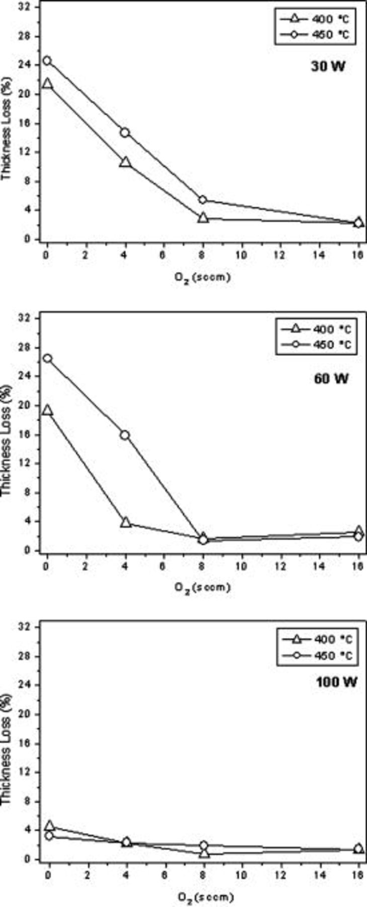
Figure 2. Thickness loss upon annealing at 400 and  for films deposited at various rf powers.
The lowest dielectric constants of 2.32 and 2.06 were obtained working at  with 4 and
  of oxygen added at the discharge, respectively, after annealing at
  . The corresponding shrinkages are 11 and 21%. Thus, there is a tradeoff between lowering permittivity and preserving good thermal and mechanical properties, as observed by other authors using different precursors.19 This means that the sample showing a slightly higher
  value but a significantly lower thickness loss is preferable and can be considered the best obtained. Samples prepared for electric measurements reported in Fig. 1 were stored in a desiccator and the dielectric constants were measured periodically over months; the values were found to be stable.
Figure 3 reports the normalized FTIR spectra of the film exhibiting the highest permittivity of 4.30 and the lowest of 2.32 for comparison. Switching from the discharge sustained at  and
and  of oxygen content in the feed to the one at
  and
and  of oxygen, an inorganic to organic crossover in deposited films is observed. In both cases the monomer flow rate was kept to
  . Spectra shown in Fig. 3a are typical of
  -like films. They display characteristic features of the Si–O–Si group: asymmetric stretching and bending mode at around 1070 and
  , respectively.20–25 The most intense absorption relative to Si–O asymmetric stretching actually shows a shoulder at around
  , which is due to disorder in the network structure. In thermal
  , the denser the structure and the smaller the number of defects, the lower the intensity of the shoulder would be. In oxides deposited by PECVD, the disorder and then the lower density of the network can be due to the presence of shorter chains induced by ion bombardment,22 stoichiometric defects due to the presence of Si–Si or Si–H bonds,23 or contaminants like N or C.21 Moreover, replacement of Si–O bonds with Si–Si has been reported to lower the bonding angles in the tetrahedral basic unit and this, together with all other defects, shifts the position of the maximum in the FTIR spectra toward lower wavenumbers.21 A weak absorption band at
  assigned to free SiOH groups is also observed.19, 24–26 Spectra do not show characteristic features of carbon-containing moieties.
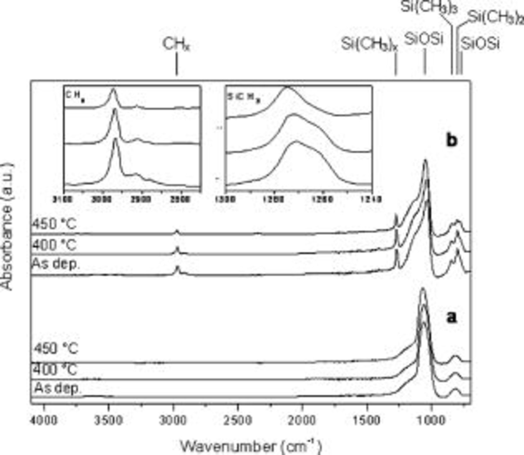
Figure 3. Normalized FTIR spectra of film deposited at (a)  ,
,  of oxygen, and (b) at
  ,
,  of oxygen.
This information was confirmed by XPS analysis, because relative carbon content in the as-deposited film was 2.2% and it diminished to 1.1 and 0.5% upon annealing at 400 and  , respectively. Considering changes in the FTIR spectra upon annealing, it can be observed that the Si–O–Si most intense absorption shifts from
  , in the as-deposited film, to
  in the film annealed at
  , and this is consistent with a rearrangement of the network toward a more ordered structure. Furthermore, the shoulder becomes progressively less pronounced and the silanol group absorption decreases as well. After the annealing at
  , the O-to-Si ratio is 1.8, the dielectric constant rises to 4.40, and the shrinkage is still limited and equal to 1.4. The deposition of highly inorganic films is in agreement with the established knowledge of organization coatings deposited at high rf power and
  /monomer ratio.
Working at  and a much reduced oxygen flow rate
  , and in turn at low
  /monomer ratio, resulted in a film with a much more pronounced organic character, as is evident from the spectra of Fig. 3b. Several features of carbon-containing moieties can be observed, e.g., at around
  the absorption due to
  stretching mode, while absorptions due to rocking mode are around
  .12–14, 16–19, 26 Finally,
  absorptions due to symmetric and asymmetric stretching are present between 2800 and
  . A deeper analysis of the
  stretching region is reported in the insets of Fig. 3b. This clearly shows that the band of the as-deposited film consists of three components corresponding to a different number of methyl groups bonded to silicon: the monosubstituted,
  , appears at
  and is a chain cross-linking group, the disubstituted,
  at
at  is a chain-propagating unit, and the trisubstituted,
  appearing at
  is a chain-terminating unit.19, 27 The presence of the di- and trisubstituted moieties is also evident from the absorptions at 803 and
  , respectively, both due to the
  rocking mode, and they partially overlap to the Si–O–Si bending mode signal at
  .13 Upon annealing at
  , the band shape of the
  is basically retained and the area decreases 20%. At
  , the band area decreases of 54% with respect to the as-deposited film and in particular the di- and trisubstituted components are drastically reduced. As a result, the maximum of the band shifts from
  , in the as-deposited film, to
  after the annealing at
  . This means that a much larger degree of cross-linking occurs into the matrix when the film is annealed at
  . Investigation of the inset relative to
  groups shows that the absorptions due to asymmetric and symmetric stretching of
  prevail and are centered at 2968 and
  , respectively. The presence of some
  groups is revealed by the small band at
  due to the asymmetric stretching mode. After annealing the
  absorption decreases but both
  and
and  components are still visible. The most intense band of the spectra assigned to Si–O–Si is broader than the ones of Fig. 3a, thus indicating a less dense, less ordered network. Moreover, the maximum is located at a lower wavenumber
  than in the highly inorganic film and is consistent with the much higher C content.24 Annealing at
  makes the shoulder less pronounced, but once more, major differences can be observed at
  where the shoulder is further reduced and the peak position shifts to
  . Atomic chemical composition as detected by XPS showed that the relative C content in the deposited film is 40.4%, and it remarkably lowers to 27.0% upon annealing at
  and to 16.7% at
  .
.
Examining the FTIR spectra of ultralow- film, it can be seen that both
  and
and  absorptions decrease upon annealing. In order to understand which moiety is released more easily, the ratio of the
  to
to  bands was calculated and results are reported in Fig. 4. It is important to keep in mind that the
  absorption band is due to hydrocarbon fragments directly bonded to Si or to those bonded to C or O. Because the ratio increases with annealing temperature, it can be concluded that silicon-bonded hydrocarbons
  are released less easily than carbon present in different form.

Figure 4. FTIR integrals ratio  as a function of annealing temperature for the ultralow-
 film deposited at
  and
and  oxygen.
Summarizing results obtained on the ultralow- film, it is important to highlight that the film just deposited already has a low-
 character, likely because it has a high amount of carbon and contains a high amount of silicon-methyl groups, which add free space to the film matrix. Upon annealing at
  , the dielectric constant is greatly reduced, even though carbon is only partially removed. This is speculated to occur because of pore formation in the film. Moreover, the limited loss of silicon-methyl groups accounts for the limited thickness shrinkage. When the annealing is carried out at
  , the dielectric constant surprisingly increases, notwithstanding the evidence that carbon is further removed from the film. This result can be explained considering that the removal of silicon–methyl groups, in this case, is more pronounced, thus leading to a greater shrinkage which in turn results in loss of free space. Starting from these outcomes, an ultralow-
 recipe can be developed where the carbon removal is necessary to form pores, but the loss of silicon–methyl groups should be limited to prevent an excessive collapse of the matrix, which leads to loss of gaps and thus an increased value of the dielectric constant.
For a better understanding of the correlation between electrical properties and chemical composition and structure of the film, the effect of rf power at different gas feed compositions was investigated. Figure 5 shows the FTIR integrals of the  band vs oxygen flow rate in the film synthesized at 30 and
  , before and after the thermal treatment. Corresponding carbon atomic percentages as determined by XPS are also reported. Importantly, the content of silicon–methyl groups in the films deposited at
  is much lower than at
  , as is shown in Fig. 5a and 5b. This suggests a more cross-linked structure that is less likely to collapse during annealing, which is consistent with the low film shrinkages shown in Fig. 2. Plots of the C content vs oxygen flow, shown in Fig. 5c and 5d, demonstrate that a greater amount of carbon is included in the film by decreasing the oxygen flow rate in the discharge. However, low
  -values in the deposited films are obtained only at
  . This difference is likely due to the large difference in
  content. When the films undergo annealing, in both cases carbon content is greatly reduced, but only at
  does this correspond to a large decrease of
  . It is argued that at
  , carbon loss does not lead to sufficient formation of pores, maybe because the cross-linked matrix is too rigid to allow the structural rearrangement necessary for pore formation to occur.
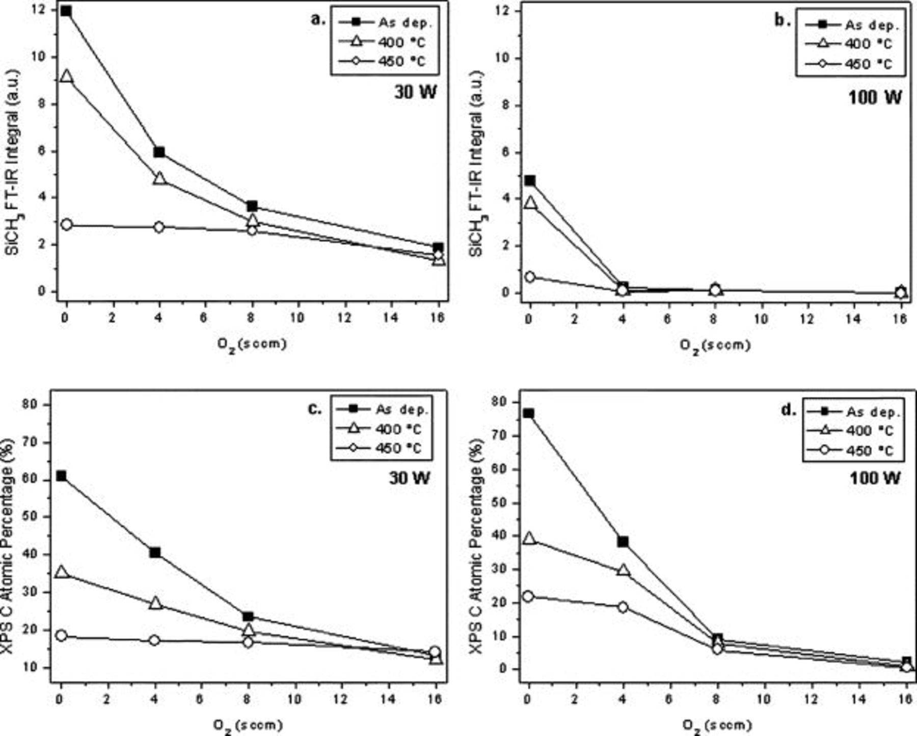
Figure 5. FTIR integrals of the (a, b)  band and (c, d) C atomic percentage as a function of oxygen flow rate for films deposited at 30 and
  .
.
In order to understand the role of the vinyl group in the film deposition mechanism and eventually, in the pore formation, FTIR spectra of the monomer (vapor phase) and of the film deposited at  without oxygen in the gas feed are compared in Fig. 6. The most interesting result is the lack of vinyl groups in the film. In fact, all the vinyl correlated bands are absent: the vinyl
  symmetric and asymmetric bands should be identified at 3020 and
  , as they occur in the spectrum of the monomer. Other characteristic absorptions are the
  stretching at
  and the vinyl
  bending at
  .6, 26, 27 The latter is maybe the only signal that is retained into the film, though it is poorly resolved. This absorption band can also be attributed to
  bending in
  groups, which can form by reaction of two vinyl groups. This is a very likely scenario due to the very low rf power used for film deposition.26 The Si–O–Si asymmetric stretching band in the monomer appears at
  , while in the film it broadens and shifts to
  , which is consistent with a less ordered structure. Moreover, the bands relative to
  and Si–O–Si at 840 and
  , respectively, are clearly distinguishable in the monomer while they partially overlap in the film. As for the
  stretching band, it is centered at
  , thus indicating two methyl groups bonded to silicon atoms. This is in perfect agreement with the monomer structure. In the film, the position and the shape of this band are the same. Finally, there is a small band at
  attributed to SiH that is absent in the spectrum of the monomer. This investigation indicates that because vinyl groups are not retained, they cannot act as a driving force in the pore formation mechanism. However, for further assessing the role of organic functionality, the discharge leading to the film with the
  value of 2.32 was repeated using HMDSO as precursor. The latter has the same structure of DVTMDSO, but with two methyl groups in place of the vinyl ones. The most striking difference is that the film synthesized from HMDSO was not ultralow-
 , as can be observed by data reported in Table II. The normalized FTIR spectra of the film before and after annealing are displayed in Fig. 7. Compared to the spectra of Fig. 3b,
  and
and  absorptions are less intense. Moreover, the Si–O–Si band is narrower with a less pronounced shoulder. In summary, films deposited from DVTMDSO are more organic: the higher content of silicon–methyl groups justifies the intrinsic lower
  of the deposited film, and the greater C contents allow for a larger number of pores to form during thermal treatment.
Figure 6. Comparison of the FTIR spectra of the monomer and of the film deposited at  without oxygen.
Table II. Comparison between electrical and thermal properties of films deposited from DVTMDSO and HMDSO.
| Sample |
 as-deposited as-deposited |
 at at 
| Thickness loss at  (%) (%) |
 at at 
| Thickness loss at  (%) (%) |
|---|---|---|---|---|---|
| DVTMDSO | 2.84 | 2.32 | 11 | 2.54 | 15 |
| HMDSO | 3.54 | 2.93 | 7 | 2.90 | 9 |
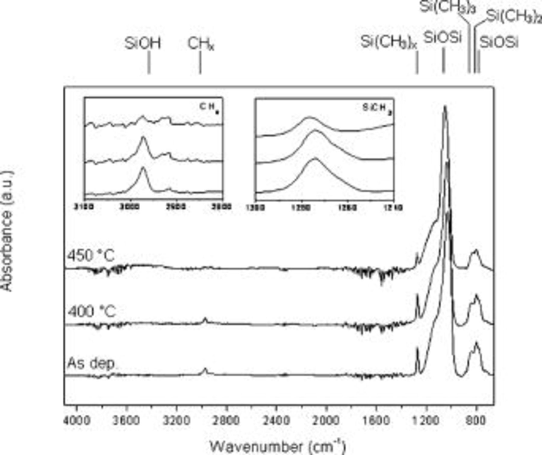
Figure 7. Normalized FTIR spectra of film deposited from HMDSO at  with
with  of oxygen. Insets show the
  and
and  bands at higher magnification.
The deposition of the ultralow- film was also performed with modulated discharges at the same peak power of
  . For this series of experiments the period was fixed at
  while the DC was varied in the range 10–100%. As is evident from data in Table III, working with modulated plasmas leads to no improvement of the electrical properties or the thermal stability of the film. Accordingly, no major differences can be seen in the FTIR spectra except for a slightly narrower Si–O–Si band in the case of film deposited in modulated conditions, which clearly is not enough to change the dielectric constant.
Table III. Electrical and thermal properties of films deposited from modulated discharges. Modulation period was fixed to  and rf peak power was
  .
.
| DC (%) |
 as-deposited as-deposited |
 at at 
| Thickness loss at  (%) (%) |
 at at 
| Thickness loss at  (%) (%) |
|---|---|---|---|---|---|
| 10 | 2.88 | 2.33 | 12 | 2.52 | 17 |
| 30 | 2.85 | 2.35 | 12 | 2.48 | 16 |
| 60 | 2.84 | 2.37 | 10 | 2.56 | 15 |
| 100 | 2.84 | 2.32 | 11 | 2.54 | 15 |
The effect of working pressure during the deposition processes on the electrical properties and on the chemical composition was evaluated. With increasing pressure from  , the dielectric constant of the deposited film decreased, as can be observed in Fig. 8. The corresponding thickness losses at
  go from 7 to 11% with increasing pressure and from 7 to 15% at
  . As for the chemical composition, normalized FTIR spectra (not reported) show that the film deposited at higher pressure has more
  groups and a higher C content. These findings relate well to the corresponding decrease of the dielectric constant and can be explained considering the milder fragmentation condition and in turn ion bombardment occurring at higher pressures.
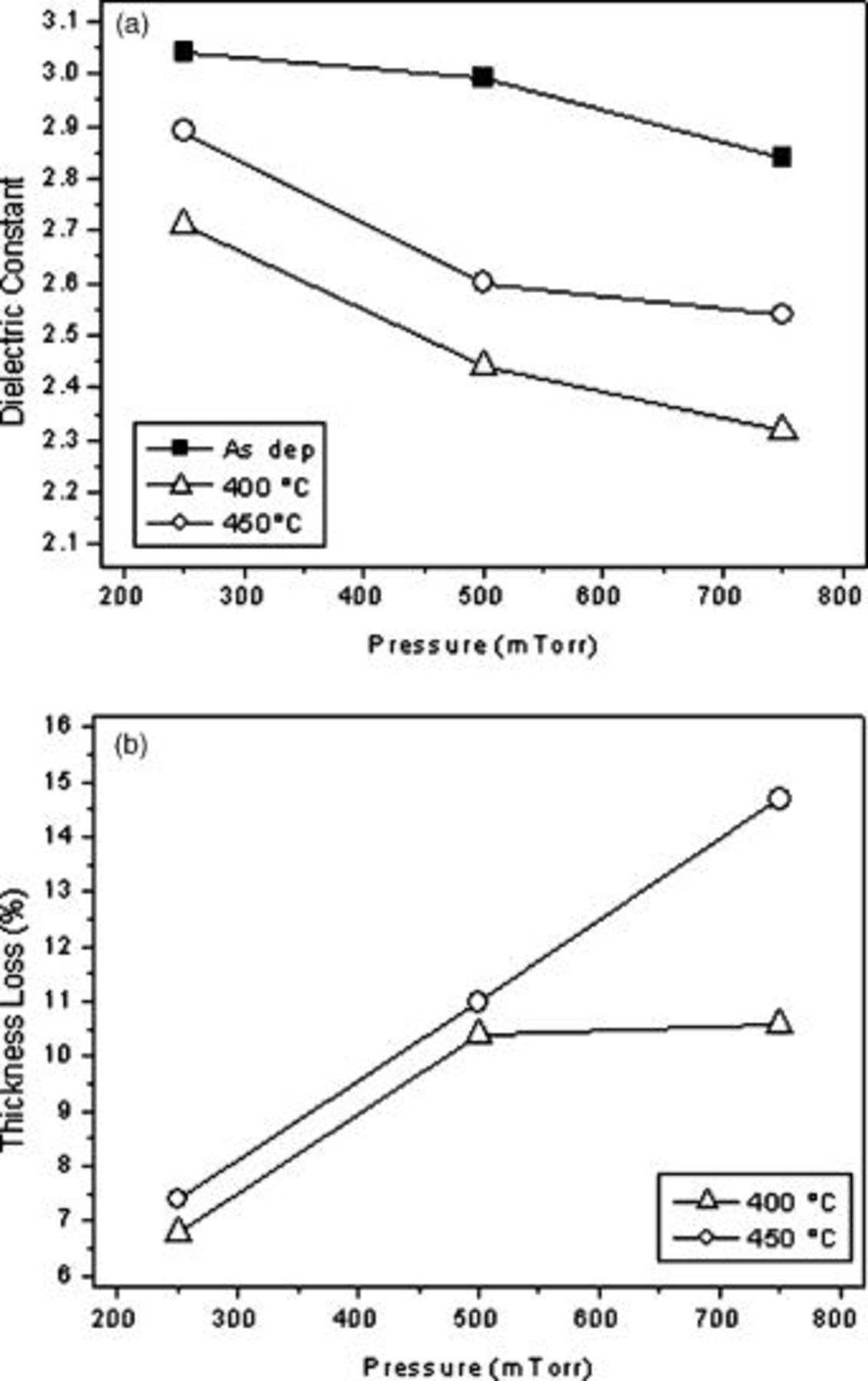
Figure 8. (a) Dielectric constant and (b) thickness loss as a function of gas feed pressure for film deposited at  and
and  oxygen.
Doubling the flux of DVTMDSO to  in the discharge at
  with
with  of oxygen results in a further decrease of the dielectric constant in the deposited film from 2.84 to 2.54. This result has to be ascribed to a larger C content in the film, as deduced by the more intense bands of
  and
and  in the FTIR spectra (not shown). When the film is annealed at
  the permittivity lowers to 2.24 with a shrinkage of 13%, similar to the 11% shrinkage obtained using
  of monomer. Again, at
  the dielectric constant increases to 2.31 and the thickness loss rises to 16%.
The deposition process leading to ultralow- film was also carried out at different substrate temperatures. Data of Fig. 9 indicate that there is an optimum temperature of
  corresponding to a minimum of the film permittivity. The thickness loss upon annealing at
  is 35% at
  , and this is very high compared to the other results obtained. At
  , on the contrary, the film loses only 2% of its thickness upon annealing. In order to understand this, normalized FTIR spectra of the film deposited at 25, 150, and
  are compared in Fig. 10. At
  the film is highly organic, as witnessed by the intense bands of
  and of
  . Moreover, the Si–O–Si band is broad and the shoulder is almost as intense as the maximum, revealing a not much denser structure. Some
  and
and  bonds are present in the matrix because of the bands at 1621 and
  , respectively, and there are some Si–H groups that absorb at
  . Going to higher wavenumbers, the absorption due to Si–OH is visible between 3200 and
  . Major changes upon annealing at
  are the strong reduction of the
  and
and  bands. In the Si–O–Si band, three different components become clearly distinguishable when observing at higher magnification: the one at
  assigned to long-chain Si–O–Si, a second band at
  due to long-chain Si–O–Si with terminal
  and –OH, and a third one at
  attributed to short chains Si–O–Si. A fourth component was also observed by other authors at
  for the short chain Si–O–Si with terminal
  and –OH.19, 28 Double bonds and Si–H groups are removed as well as hydroxyl groups. When switching to
  it is clear that the film is much more inorganic because of the low C content and the much less intense shoulder of the Si–O–Si band. No big differences are noticed in the spectrum when the film is annealed. On the basis of the last observations, it can be concluded that the film deposited at
  is the best compromise between a carbon-rich film that then collapses upon annealing, and a silica-like film that does not allow the formation of enough pores to get ultralow-
 values.

Figure 9. Effect of deposition temperature on the dielectric constant of film deposited at  and
and  oxygen.

Figure 10. Normalized FTIR spectra of the film deposited at different temperature with rf power fixed at  and oxygen flow rate of
  , before (straight line) and after (dashed line) annealing at
  .
.
In a final series of experiments the annealing temperature was varied and the effect on the dielectric constant was studied. The curve of Fig. 11 shows a minimum of the  value when the annealing is performed at
  . As the temperature is increased from
  , infrared spectra (not reported) show a continuous decrease in the C content. Correspondingly, the film thickness loss gradually increases. These results can be rationalized considering that at
  the carbon released is too low and not too many pores form, which is why the decrease of the dielectric constant is quite limited. When the temperature is increased at
  , enough gaps are created in the structure with still quite reasonable shrinkage, but by further raising the temperature the matrix collapses too much, thus reducing the overall free space and consequently, the dielectric constant increases. The ultralow-
 sample was also annealed at
  for
for  instead of
  and both dielectric constant and thickness loss were found to be the same.
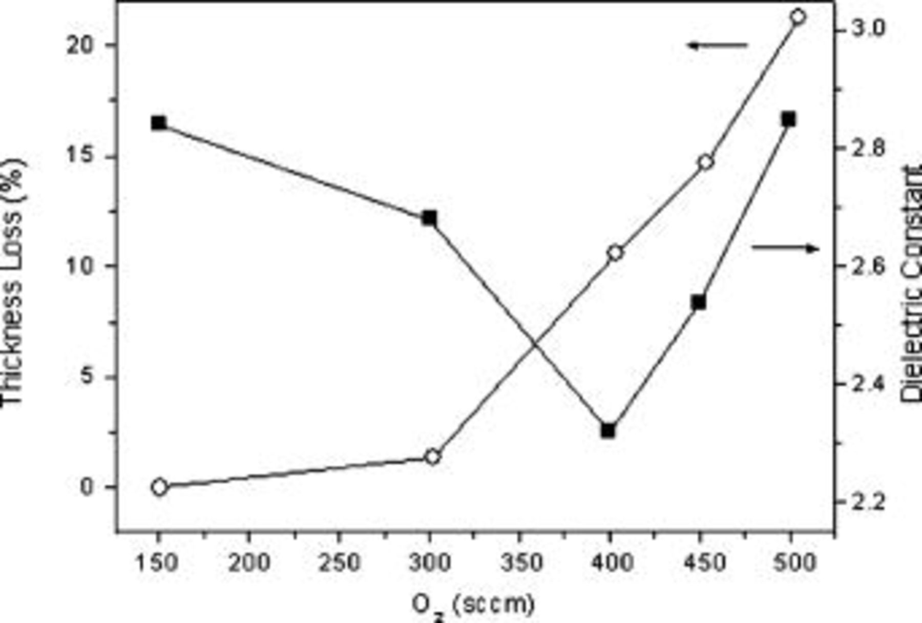
Figure 11. Effect of the annealing temperature on the ultralow- film-deposited at
  and
and  oxygen.
For a deep analysis of the annealing process, a TG–MS analysis was carried out on the film with the lowest  . The TG curve of Fig. 12 shows that the mass loss occurs in three subsequent steps centered at 170, 400, and
  . The weight loss is 2.2% at
  and 4.3% at
  . On the basis of these data, mass spectra at
  were first examined. After peak assignation, molecular species evolution was studied from spectra recorded vs time (i.e., different temperatures). In Fig. 13 profiles of the hydrocarbon fragments released during pyrolysis, the structure of which is compatible with the
  values observed in the MS spectra, are reported. Profiles are grouped depending on the parent peak the ions come from. For example,
  and
and  are believed to come from a further fragmentation of
  during MS analysis. Once normalized, their trends perfectly overlap. Moreover, the fragmentation pattern of
  reported in literature29 shows peaks due to
  and
and  , as well. Interestingly, longer hydrocarbon fragments are released before shorter ones, because maxima of group C5 appear before those of C4 and C3 and C2, and this is consistent with higher Si–C binding energy for shorter chains.30 This result suggests that longer hydrocarbon fragments apparently are dangling chains more easily lost during annealing, thus allowing formation of free space in the matrix. In accordance with results discussed so far, Si-containing fragments were also detected during pyrolysis, as reported in Table IV, resulting in partial collapse of the polymer structure.

Figure 12. TG on the ultralow- sample deposited at
  and
and  oxygen. Arrows indicate the steps in which mass loss occurs during annealing.
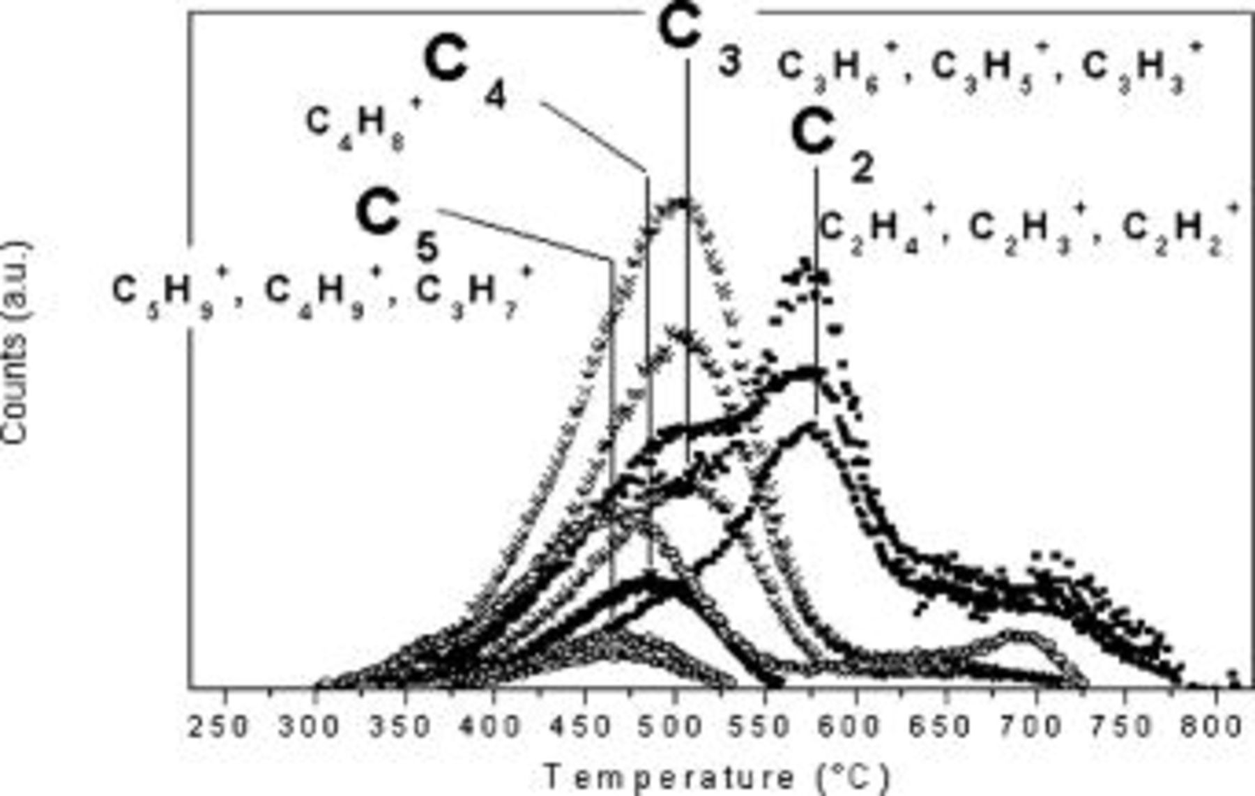
Figure 13. Temperature evolution of hydrocarbon ions detected by mass spectrometry.
Table IV. Proposed silicon-containing fragments released during pyrolysis.

| Assignment |
|---|---|
| 75 |
|
| 119 |
|
| 120 |

|
| 133 |
|
| 134 |

|
| 193 |
|
Conclusions
Low- to ultralow-
 films were deposited under various experimental conditions from DVTMDSO glow discharges, mixed with oxygen and argon as carrier gas.
Electrical properties, thermal stability, and film chemical composition and structure were found to be strictly dependent on the discharge parameters used during the deposition. Ultralow- materials were obtained by working at low rf power and adding a small flux of oxygen to the gas feed. It was shown that a trade-off exists between reduction in permittivity and preservation of good thermal and mechanical properties, which prompted a comprehensive study of both the deposition step and the thermal treatment. The best result obtained is a dielectric constant of 2.32 with a thickness loss of 11%. Dielectric constants as low as 2.06 were observed, but these films demonstrated unacceptably large shrinkage values. The most important outcome was that it seems there is an optimum organic character and degree of cross-linking that films should exhibit that allow for the formation of sufficient pores upon annealing without excessive shrinkage. Large film shrinkage values were indicative of a matrix collapse, which rules out the inclusion of pores and thus increased the dielectric constant and poor mechanical properties. Therefore, the ongoing challenge in this field of research is no longer to simply achieve ultralow-
 values but to gain control over the associated thermal and mechanical properties as well for materials to be successfully integrated into IC manufacturing processes.
Besides low rf powers and low oxygen flow rate, it has been demonstrated that high process pressure is necessary to get to extremely low permittivity values while maintaining good thermal stability. Moreover, the deposition temperature strongly affects film properties. At room temperature, in fact, the film is too organic in nature and consequently during thermal treatment too many alkyl groups are lost, resulting in matrix collapse. Higher deposition temperatures, i.e.,  , however, lead to a highly inorganic film. In that case, because of the low carbon content, few pores form and the result is a low-
 film with very limited thickness loss.
Doubling the monomer flow rate was effective in lowering the  value of the deposited film, which then further decreases to 2.24 upon annealing, with a shrinkage of 13%. Annealing temperature was also found to play a key role in determining the dielectric constant. At low anneal temperatures, in fact, the carbon removal necessary to form pores is small and a low-
 film is obtained. By increasing the temperature the number of pores increases as well as the thickness loss. When the pore content is too high, structural collapse occurs, which results in an increased dielectric constant. Best results are then obtained at the intermediate temperature of
  . Additional examination of the annealing step by TG–MS revealed that longer hydrocarbon fragments are released before shorter ones and Si-containing fragments are released as well, which are responsible for the matrix collapse.
It can be concluded that the presence of thermally sensitive (removable via annealing) functional groups (e.g., vinyl) in the monomer is essential, and including a porogen component in the deposited films allows extremely low permittivity values to be reached.
Acknowledgments
The authors gratefully acknowledge Vincenzo Colaprico, Vincenzo Bonasia, and Savino Cosmai for their technical assistance.
The University of Bari assisted in meeting the publication costs of this article.