
Abstract
This work describes a procedure based on a mixed template of copolymer F127  and surfactant CTAB (cetyltrimethylammonium bromide) for generating anatase
  nanocrystals. When the particle size is 3-5 nm, the surface area without aggregation is about 300 m2/g, but our experimental value is 180 m2/g. This means that not all surfaces of 3-5 nm particles are exposed. Then the prepared
  nanocrystals were used to assemble dye-sensitized very thin solar cells of about 6 μm. Its photocurrent-voltage performance was investigated. The mixed template allowed the fabrication of crack-free porous
  film electrodes of various thicknesses by repetitive coating and calcinations. The transparent solar cell obtained with a six-time repetitive coating exhibited an open-circuit potential of
  a short-circuit photocurrent density,
  a fill factor,
  and an efficiency of
  A solar cell using the commercial P25 as the
  film electrode was also assembled for comparison, and the result are analyzed and discussed. © 2004 The Electrochemical Society. All rights reserved.
Export citation and abstract BibTeX RIS
In recent years, solar cells based on photoelectrochemical dye sensitization of mesoporous semiconductive oxide electrodes have been regarded as regenerative low-cost alternative cells for conventional solid-state devices, and they have attracted considerable academic and practical interests.1
2
3
4 Among these materials,  nanocrystalline electrodes have been investigated extensively as a key material for the dye-sensitized solar cells (DSC). The high performance of DSCs required a porous
  film electrode with large surface area, highly crystalline, and without crack and cavities, so that the dyes can be sufficiently adsorbed and the electrons can be quickly transferred. In recent decades, many methods have been developed to fabricate DSCs based on nanoporous
  film prepared by a hydrothermal treatment or based on a commercial
  (P25). However, almost all these methods need to disperse
  nanoparticles in water with specialized and complicated equipment and techniques. Also, due to incomplete dispersion, it is difficult to avoid the aggregation of particles which may result in the crack and cavities in the electrode film, especially for commercial
  (P25) particles, which resulted in low energy conversion efficiency in the DSCs.5 On the other hand, in order to increase the dye adsorption and improve the charge injection, thick DSCs of over 10 μm even tens of micrometers were usually needed to be fabricated. However, it is very difficult for the fabrication of a thick film by traditional coating methods with a dispersed
  paste source. Also the thick film limits the permeation of incident light and improved efficiency. The aims of this report are, therefore, to establish a chemical technique by making a gel that would replace the conventional physical mechanical dispersion methods and make it much easier to fabricate the DSCs and overcome the defect of the traditional method. The gel can be freely and easily coated on the surface of substrates to form transparent
  film electrodes of various thicknesses, shapes, and high efficiency.
There are many routes for the creation of nanocrystalline oxides, among which the template synthesis method has been playing an important role, especially for those with various surface and crystalline properties. The copolymer, with its special self-assembly characteristics, has been acknowledged as a crucial template for the preparation of materials with novel properties and morphologies.6
7
8 Moreover mixed templates have been used to control the structure and properties of materials. By simply mixing one neutral surfactant with an ionic one as the template, Ryoo et al. have synthesized a long-term, stable mesoporous silica with a high yield.9 Furthermore, the mixed template can exhibit very complex phase behavior in an aqueous solution and yet has been expected to be used to form new products with varied structures and improve the properties of known materials. Here,  gel with anatase phases was prepared by using a mixed template and then directly used to fabricate the DSC. In our work, the mixed template agents not only play the role of a template, which formed the porous structure, but also are responsible for the fabrication of homogeneous
  gel, which is crucial for the preparation of film with uniform and crack-free structure and various thicknesses. So it is very important to select a suitable template for making high-performance
  film and improving the efficiency of the DSC. Taking into account these considerations, we select copolymer F127 produced by BASF Company, an excellent gelation and coating agent, as our template with good qualities for the formation of a homogeneous gel. Meanwhile, based on the consideration of mixed systems of polymers and surfactants, which have been studied extensively10
11
12 and suggest that some selected surfactant could strongly interact with the polymer to form micelles of various shapes and sizes, we selected another surfactant, CTAB, as another template. The complex formed in the mixed system of polymer and surfactant has been expected to be a new template for the preparation of materials with novel structure and properties.
film and improving the efficiency of the DSC. Taking into account these considerations, we select copolymer F127 produced by BASF Company, an excellent gelation and coating agent, as our template with good qualities for the formation of a homogeneous gel. Meanwhile, based on the consideration of mixed systems of polymers and surfactants, which have been studied extensively10
11
12 and suggest that some selected surfactant could strongly interact with the polymer to form micelles of various shapes and sizes, we selected another surfactant, CTAB, as another template. The complex formed in the mixed system of polymer and surfactant has been expected to be a new template for the preparation of materials with novel structure and properties.
In this paper, we describe a mixed template method to synthesize nanocrystal anatase  and a new coating technique to fabricate the DSC. This process provides a simple way to fabricate crack-free porous
  electrode film of any thickness.
Experimental
Materials.—
Conducting glass plates (indium tin oxide, ITO, Geomatec Co. Ltd.) were used as the substrate for depositing nanocrystalline  electrodes. Tetraisopropylorthotitanate (TIPT), acetylacetone (ACA), LiI, CTAB (Wako Chemicals), F127 (BASF), cis-di(thiocyanato)-
 -bis(2, 2'-bipyridyl-4-carboxylate-4'-tetrabutyl ammonium carboxylate) ruthenium(II), (N719; Solalonix), tert-buthylpyridine (TBP), and dimethylpropylimidazolium iodide (DMPII) (Shikoku kasei) were used as received.
Preparation of the  electrode.—

A mixed template was composed of copolymer F127 and surfactant CTAB. The  gel for electrode preparation contained the hydrolyzation and condensation of TIPT. First, 6.8 g of tetraisopropyl orthotitanate (TIPT) was mixed with 2.4 g of acetylacetone (ACA) to form a stock solution, which was added to 60 mL mixed template solution with a fixed amount of F127 (10 wt %), and various concentrations of CTAB. The final solution
  was stirred at 40°C until a uniform transparent solution was obtained. Then the resulting solution was kept at 80°C in a closed container for three days and formed a bright yellow
  gel. Finally some of the
  gel was directly calcined at 450°C for 2 h under ambient atmosphere to remove the templates and the thus formed white nanoscale
  was used for taking measurements such as X-ray diffraction (XRD) and transmission electron microscopy (TEM). For the preparation of photoelectrodes, several drops of
  gel were spread onto the conducting glass substrate
  using a glass rod with adhesive tape (Scotch, ∼40 μm thick) as the spacer. We fabricated thick
  films by repetitive coating and calcining at 450°C for 10 min. At last, the film was calcined at 450°C for 1 h before DSC fabrication and film thickness measurement.
Fabrication of dye-sensitized solar cells.—
After sintering at 450°C for 1 h, the porous  electrodes were cooled to about 80°C, and immersed in an ethanol solution of a ruthenium complex (N719) over 24 h for dye adsorption. The dye-adsorbed
  electrodes were assembled like a sandwich with a counter electrode (a platinum-sputtered ITO glass) held by clamps. A drop of electrolyte solution (0.1 M LiI, 0.6 M DMPII, 0.05 M
  and 0.5 M TBP in methoxyacetonitoryl) was introduced into the clamped electrodes.
Measurements.—
The crystalline phase of  and its particle size were determined by XRD (Rigaku Goniometer PMG-A2-CN2155D2) with Cu Kα radiation at a scan rate of
  The average crystallite size was calculated according to the Scherrer equation. The morphology of samples was examined by TEM (JEOL 200CX, operated at 200 kV). The specimen for TEM imaging was prepared by suspending 2 mg of the powder sample with ethanol and sonicating it in an ultrasonic bath for 30 min. The Brunauer-Emmett-Teller (BET) surface area
  and pore size distribution of the samples were determined using a BEL SORP 18 PLUS nitrogen adsorption apparatus with all samples degassed at 200°C for 2 h before the actual measurements. The morphology and thickness of the mesoporous
  electrodes were characterized by scanning electron micrograph (SEM, JEOL, JSM-5510). Photocurrent-voltage measurements were performed using an AM 1.5 solar simulator (100 mW/cm2, Oriel, 1000W9112). The cell size was 0.25 cm2. The cells made of P25, a commercial
  -containing anatase and rutile phase, were also prepared for comparison.
Results and Discussion
The physicochemical properties and morphology of powder samples.—

Table I shows the synthesis conditions and the corresponding physicochemical properties of the as-prepared  particles. It clearly shows that the surface area of
  particle was very large, and varied with the concentration of CTAB in the mixed templates in which the concentration of F127 was fixed at 10 wt %. The as-prepared
  particles were very small with an average size of 3-5 nm, depending upon the concentration of CTAB in the template. The
  particle with the smallest average size of 3.58 nm was obtained in 0.1 M CTAB. Figure 1b shows a typical TEM image of
  particles prepared in the template system. It reveals that the nanocrystals have a relatively spherical shape with a size distribution of 3-5 nm. Figure 1a showed the XRD patterns of the
  particles calcined at 450°C for 2 h. Clear and intensive anatase patterns according to JCPDS card 21-1272 are observed in different systems, and the shape of the patterns are similar to each other. The diffraction intensity gradually increased with the concentration of CTAB in the 10 wt % F127 mixed template, which suggested increasing crystallinity in these materials. The size of particles calculated by Scherre equation is below 5 nm and are shown in Table I which agrees well with the results of TEM observation. It indicates that the
  particles are primary particles with excellent dispersibility and stability even with heat-treatment. Figure 1c is a high-resolution TEM image of sample B. It shows that all the primary particles are highly crystallized and the crystal growth according to the mechanism of oriented attachment13 does not occur during calcinations. That is due to the use of the mixed template which restricted the attachment and aggregation of primary particles and kept the growth of crystals. These results indicated that the template drastically affects the size, surface area, and crystallinity of
  particles. In the present case, copolymer F127 promoted the homogeneity of the mixture solution and hindered the aggregation and recombination of the neighboring
  crystalline nucleus in the formation and calcination processes, just as reported in the literature.14 However, the size of the resultant particles is below 5 nm, which is smaller than the micelle size formed in single copolymer F127 without CTAB. It is expected that surfactant CTAB has modified the micelle structure and resulted in the formation of smaller nanocrystals, which is in accordance with the reports in the literature.10
11
12 In these studies, Chari et al.10 and Griffiths et al.11 found that some selected surfactant could strongly interact with the polymer to form micelles of smaller size. In our work, the CTAB surfactant and copolymer F127 are expected to have been incorporated with each other which leads to the reduction of the size of the produced particle in the mixed template system. Because of its high surface area and high crystallinity, all the as-prepared samples have a quantum confinement effect and high photocatalystic activity. Considering the surface area and size of particles, we selected sample B with the largest surface area and the smallest size to prepare
crystalline nucleus in the formation and calcination processes, just as reported in the literature.14 However, the size of the resultant particles is below 5 nm, which is smaller than the micelle size formed in single copolymer F127 without CTAB. It is expected that surfactant CTAB has modified the micelle structure and resulted in the formation of smaller nanocrystals, which is in accordance with the reports in the literature.10
11
12 In these studies, Chari et al.10 and Griffiths et al.11 found that some selected surfactant could strongly interact with the polymer to form micelles of smaller size. In our work, the CTAB surfactant and copolymer F127 are expected to have been incorporated with each other which leads to the reduction of the size of the produced particle in the mixed template system. Because of its high surface area and high crystallinity, all the as-prepared samples have a quantum confinement effect and high photocatalystic activity. Considering the surface area and size of particles, we selected sample B with the largest surface area and the smallest size to prepare  film electrodes.
Table I.
Synthesis condition and physicochemical properties of  particles. particles. | |||||
|---|---|---|---|---|---|
| Sample | 10%  | Crystallite size (nm) |
 | Pore volume(mL g−1) | Pore size (nm) |
| A | 0.05 | 4.62 | 150.12 | 0.542 | 4.32 |
| B | 0.1 | 3.58 | 185 | 0.677 | 4.97 |
| C | 0.25 | 4.13 | 167.69 | 0.604 | 5.22 |
| D | 0.5 | 4.62 | 143.98 | 0.205 | 6.58 |
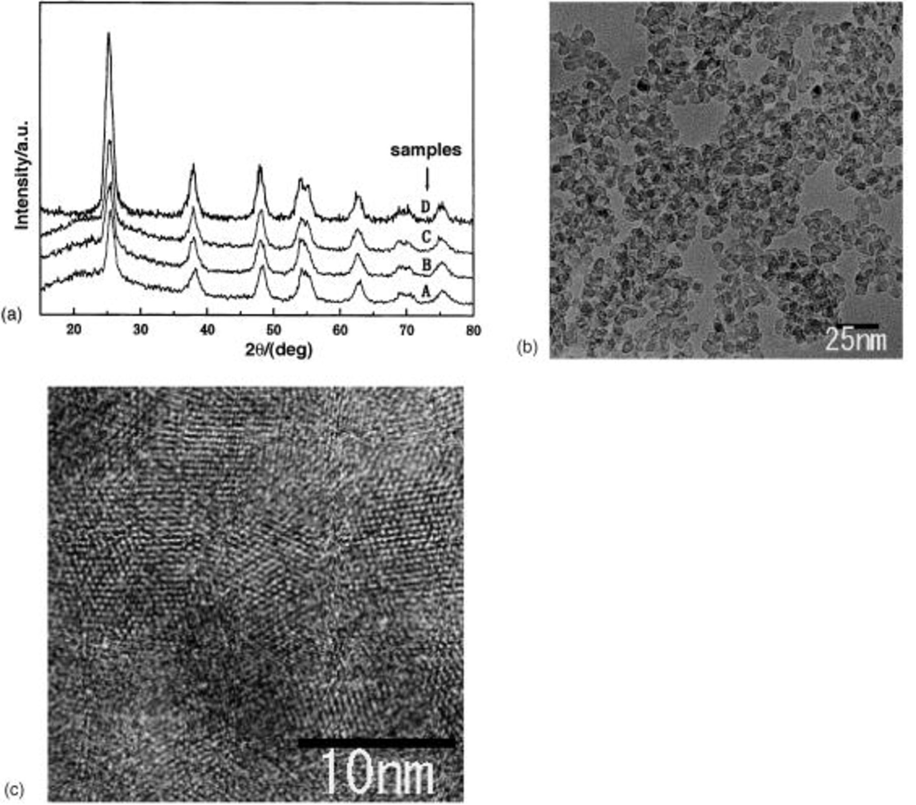
Figure 1. (a) XRD patterns of samples A-D, (b) a typical TEM image of sample B, (c) high-resolution TEM image of sample B.
The morphology of nanocrystalline film.—

Figure 2 shows the SEM images of the surface morphology and the cross section of  film with different coating times after calcinations at 450°C for 1 h. The thickness of porous film with the first coating is about 1.1 μm (Fig. 2a).
  film with 3.2 μm thickness is obtained after three coatings (Fig. 2b). Eight coatings makes a
  film with a thickness of 8.2 μm. It indicated that almost the same thickness of film is fabricated with each coating. Figure 3 shows the thickness as a function of the number of coating times. The film thickness was increased monotonically with the coating times in the two film series. Curves a and b correspond to different concentrations of Ti in the gel, the former is 0.4 M and the latter 0.2 M. However, the increasing rate is slightly deaccelerated over the six coating process. Moreover, it is clear that no crack or gap can be observed between each coating layer, and the surface of each layer is very smooth and homogeneous without cavities and cracks, although the film was not made by a one-time coating process. (Fig. 2f-h). Figure 2j shows a high magnification SEM image of surface morphology with the eight coating processes which reveals that no clear change can be observed in the size of particles. These results indicated that using a mixed template effectively avoided cracks in the film and maintained the homogeneity and also prevented the aggregation of particles in coating and calcination. Also the burning and decomposition of the mixed templates in calcinations makes the film a porous structure which is suitable for the solar cell electrode (Fig. 2f-j). From the comparison of transmittance between the coated electrode and the substrate, we can show that the film is transparent in the visible light range even with eight coatings (shown in Fig. 3 inset). As is well known, light scattering and light absorption are both factors that decrease optical transmission. The transmittance decrease in the ultraviolet range is caused by the absorption of
  Light scattering in our system is avoided by forming a homogeneous phase film with small size particles stuck together and phase separation is prohibited. In our work, the electrode can be formed with perfect transparency although it may not be the best condition for high-efficiency DSC, which is illustrated in the end of this paper.
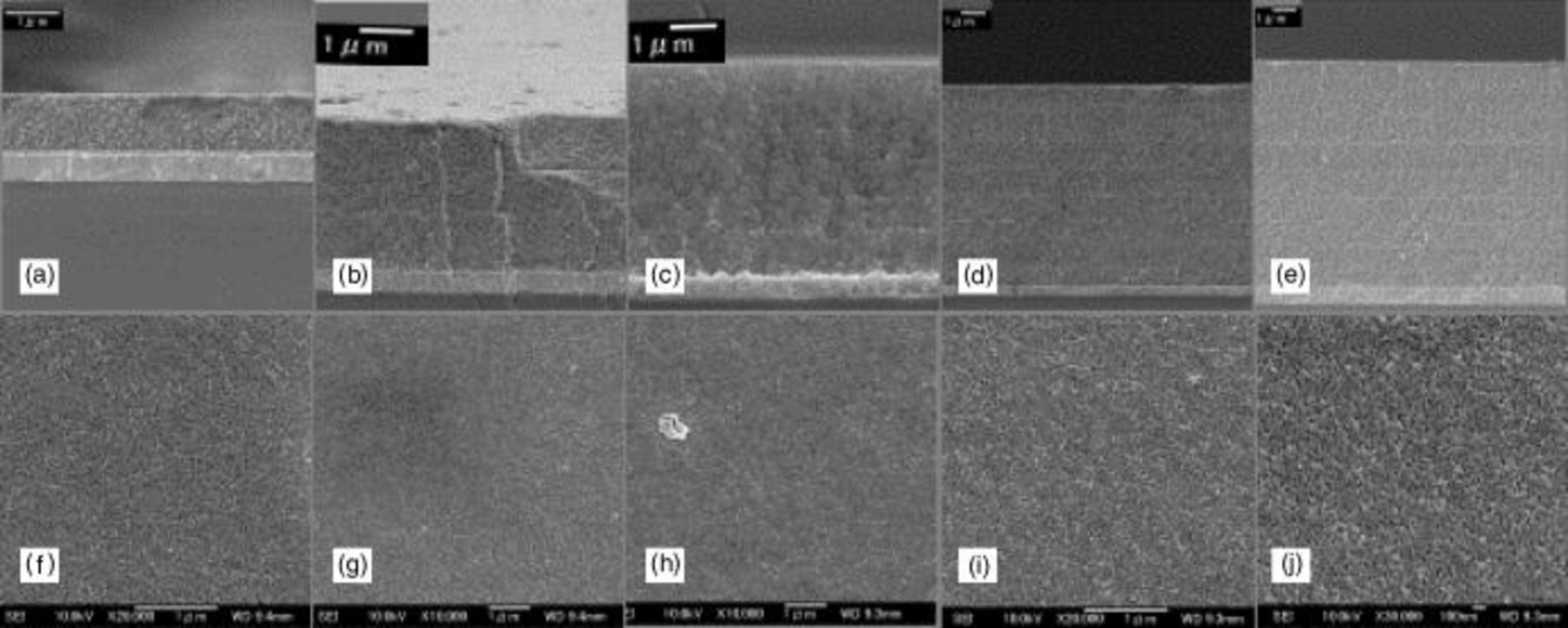
Figure 2. SEM images of  film coated various times showed the cross section of (a-e) and the surface morphology (f-i). The number of coats are (a, f) one, (b, g) three, (c, h) five, (d-i) eight, and (e) nine. (j) High-resolution image of the surface coated eight times. Scale bars are (a-i) 1 mm and (j) 100 nm.
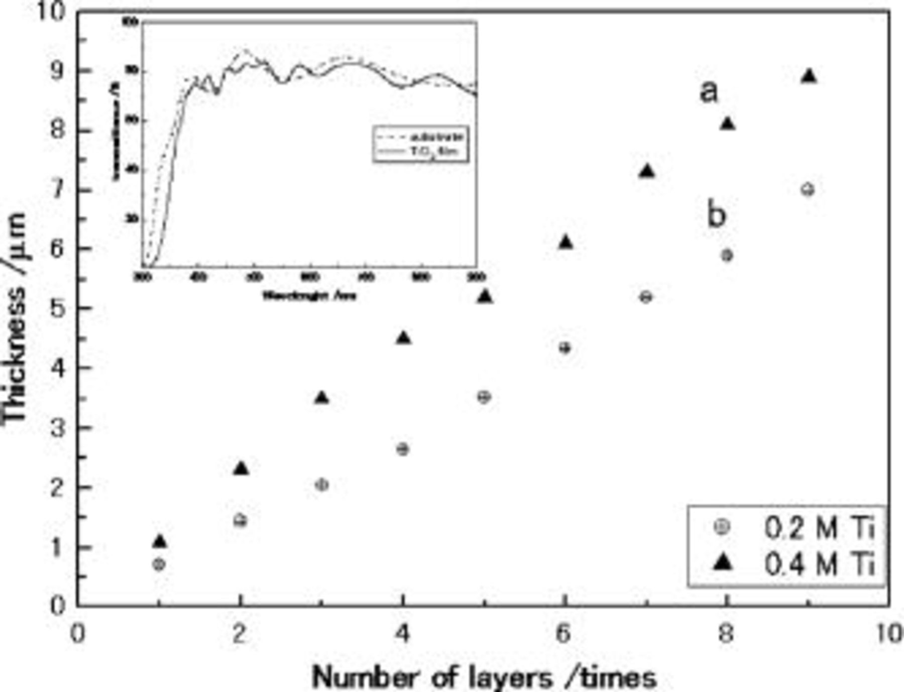
Figure 3. The dependence of thickness of  film on repetitive coating times, and transmittance spectra of substrate (dotted line) and
  film (solid line) (insert).
All the SEM images show a fine crack-free  porous electrode without a distinct cavity which can be attributed to the perfect coating characteristics of the gel and also the coating technique. From the second layer coating, the
  gel is coated on the still hot substrate, the temperature is about 80°C which is the formation temperature of
  gel in the preparation. Because the mixed template of F127 modified by CTAB keeps excellent gelation properties at this temperature, the
  gel is immediately dried and tightly attached into the underlayer, which avoids the formation of gaps between two layers and crack or cavities with each coating in comparison with the traditional dispersed technique in which the crack and cavities are often formed due to incomplete dispersion and unsuitable composition of the paste. Meanwhile, the removal of the mixed template by evaporation followed by calcinations produced a finely porous structure in the film, which can be observed in the SEM images even with thick film (Fig. 2f-j). The SEM images also indicate that the porous structure is formed with each repetative times coating, drying, and sintering and does not vary with the increasing thickness of the film. Of course, the size of the pores would shrink with increasing heat-treatment time and temperature as reported.15 In our work, when the coating is repeated over six times, the thickness of each coating is decreased which is expected to be due to the shrinkage of the porous structure in the underlayer with continuous heat-treatment. However, the homogeneous
  gel with very small size pores prepared with the mixed template has avoided the cracks in the film and gives a perfect porous electrode. With this property, the
  gel can be used to make film with large thickness depending on the number of coatings.
Dependence of I-V curve on coating times.—
The performance of the DSC can be characterized by measuring the current-voltage curves of the prepared DSC from which the light-to-electricity conversion efficiency can also be achieved. Figure 4a shows the dependence of the light-to-electricity conversion efficiencies (η) on the repetitive coating times of  films. Each measurement was carried out using six
  electrodes to confirm the reproducibility. The conversion efficiency of the
  film at the one-time coating was 3.2-3.6%. The η of DSC increased monotonically with the thickness of the film till the six coatings, and decreased from seven coatings. At the six coatings η became 8.3%, which is about 2.5 times higher than that of the one-time coating process. Figure 5 shows the current-voltage characteristics of the dye-sensitized solar cell with a
  film coated six times (about 6.1 μm thickness). The open-circuit photovoltage
  the short-circuit photocurrent
  the fill factor, and η were 760 mV, 17.2 mA/cm2, 0.635, and 8.3%, respectively. The efficiency was far higher than mesoporous
  electrodes made from commercial P25 with the same thickness. Also the latter can not be coated many times due to the cracks and gaps produced between or in the layers.
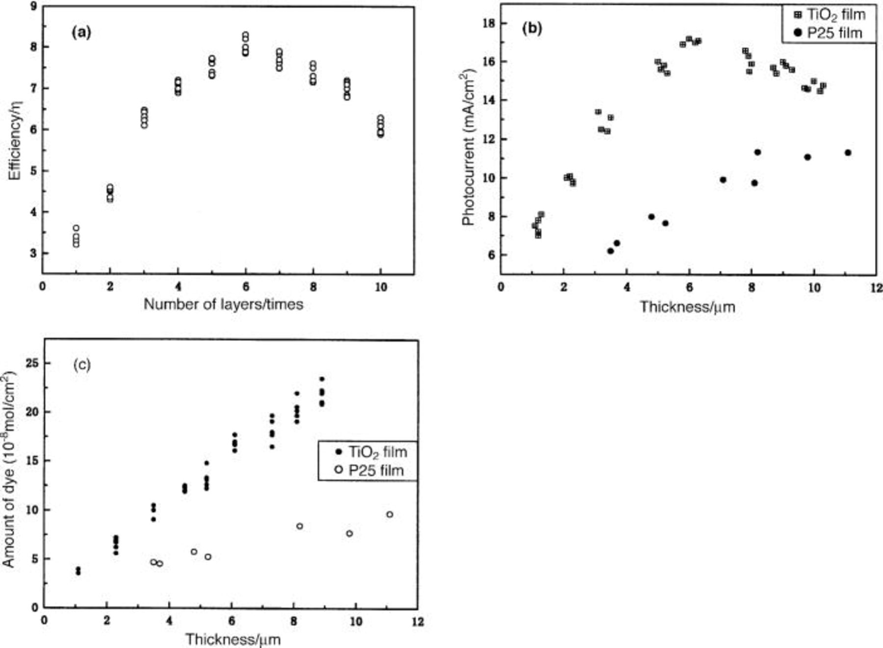
Figure 4. (a) Dependence of efficiency and the repetitive coating times. Photocurrent (b) and amount of dye (c) as the function of thickness of film of  and P25.
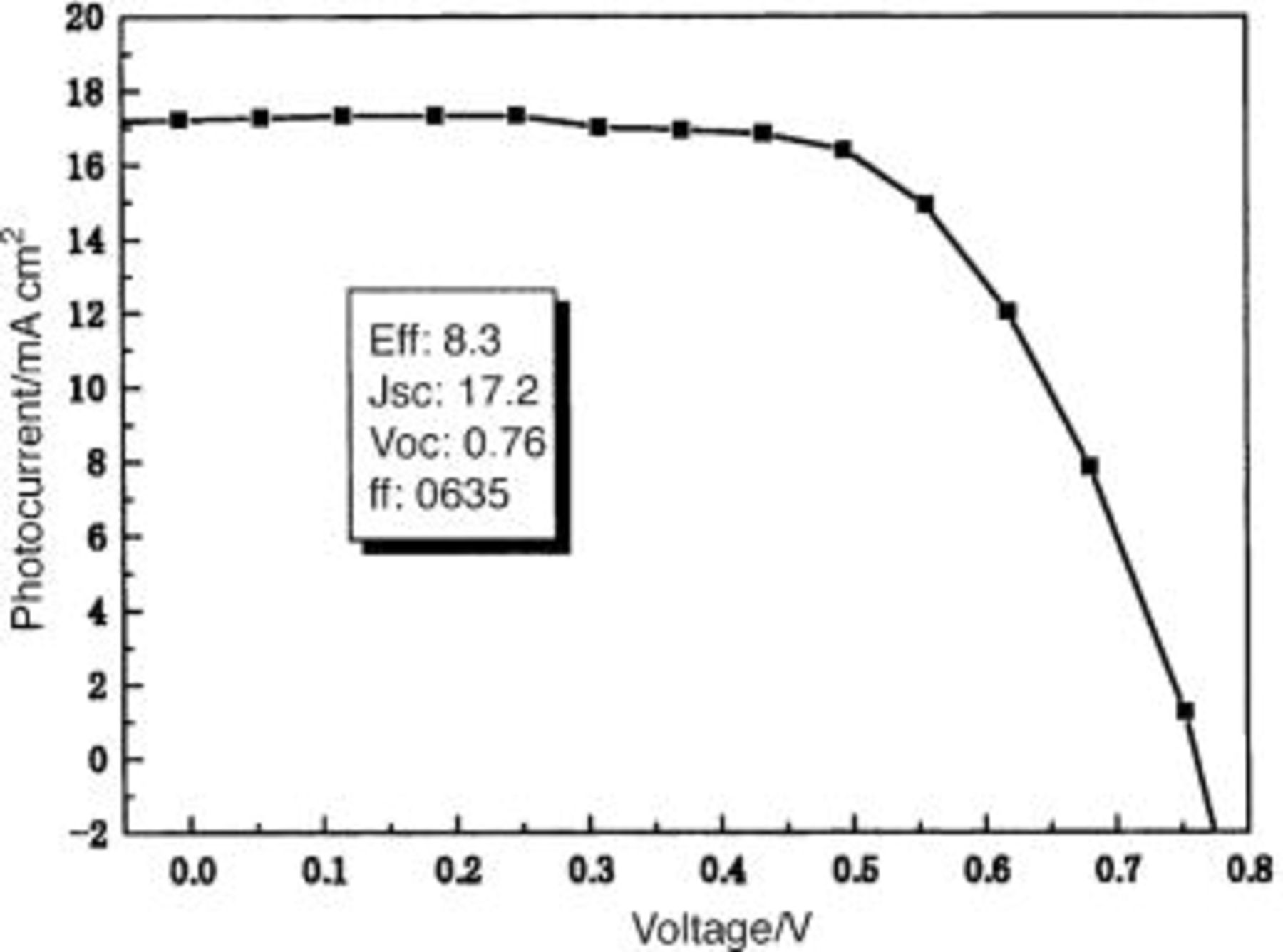
Figure 5. Photocurrent-voltage characteristics of the dye-sensitized solar cell with a  film coated six times.
Figure 4b shows the dependence of the short-circuit current  on the thickness of the film prepared with the
  gel prepared in this work and also commercial P25. It is clear the
  of the DSC prepared in our work is far higher than that of P25 electrodes with the same thickness. However, when the thickness of the film is over 7 μm, the efficiency and photocurrents are generally decreased. These results are different from some other reports, in which the thick
  is an ideal candidate for high conversion efficiency in DSC.1
2
3
4
5 The amount of dye adsorbed in the film is increased monotonically even over the thickness of 7 μm (Fig. 4c). The difference between our work and others must be due to the size of our prepared
is an ideal candidate for high conversion efficiency in DSC.1
2
3
4
5 The amount of dye adsorbed in the film is increased monotonically even over the thickness of 7 μm (Fig. 4c). The difference between our work and others must be due to the size of our prepared  particles and the porous structure of the prepared film. The
  particles prepared in this work are much smaller than those produced in previous work,1
2
3
4
5 so in our DSC the
particles prepared in this work are much smaller than those produced in previous work,1
2
3
4
5 so in our DSC the  can adsorb more dye than that produced with larger size particles with the same film thickness. Thus, when the thickness is over 6 μm, the
  film might have adsorbed enough dye so that the quantity of adsorbed dye is not the decisive factor for efficiency any more. Because of the relatively small size of the particle, the electron transfer impedance can be much larger due to more sticking points between particles which hinder the electron diffusion in the nanoporous
  film electrode. Moreover the thick film increased the diffusion resistance of the electrolyte, especially the large
  ions, which increased the opportunity for the recapture of an electron by
  and resulted in decreased efficiency. As we have shown, the average pore size of film depended on the average size of the aggregation crystals that have been formed after calcinations. In our work, the average pore size is very small due to small particle size (3-5 nm) and less aggregation during calcinations which is due to the mixed template used. From the SEM image and
  adsorption measurement, the pore size of the porous
  film is just about 4-6 nm. In such small pores, after the dye has been adsorbed in the porous film, 3 nm are occupied by the dye molecules (molecular diameter of 1.5 nm) that adsorbed on the pore walls, which leaves an aperture of only 1-2 nm for the diffusion of the electrolyte. This distance is very similar to the size of the
  ion which makes the diffusion of electrolyte become the limiting step under this condition. This has been verified by Gratzel et al. 's research and has been illustrated in detail.15 Considering the mechanism of the DSC, we can conclude that the thickness of the
  film has an opposite bifunctional character as increasing the dye adsorption as well as increasing the diffusion resistance of the electron and electrolyte. The DSC is a rather complicated system including such processes in series as light adsorption, charge injection, charge collection, and electrolyte diffusion. There are many factors that influence the resultant light-electricity conversion efficiency of DSC. So the high efficiency cannot be achieved by optimization of only one or two factors and processes. The DSC must be considered as a whole in order to obtain a high efficiency DSC. Using our method we can make a highly transparent electrode with adequate thickness. But this does not mean that high transmittance is the best condition for DSC because it increases the loss of light energy. In our work, the high transmittance electrode may be one reason for not having obtained higher efficiency DSCs. It has been suggested that adding a top scattering layer, which can sufficiently scatter and use the limited light may be a better way to increase the efficiency of our DSC. The effect of a scattering layer will be investigated in further work.
Conclusions
In summary,  gel was prepared with a mixed template of F127 and CTAB, which fabricated high-performance nanocrystals
  with sizes of 3-5 nm and a high surface area. With a repetitive coating technique, the prepared
  gel is coated and forms homogeneous and transparent DSC film electrodes of various thicknesses, which give rise to the high conversion efficiency of light to electricity with a thin-film electrode (about 6 μm). This method is very easy and avoids the complicated dispersion steps of
  particles and maintains the primitive properties of
  nanocrystals prepared with the mixed template method.
Acknowledgments
The authors gratefully acknowledge Professor S. Isoda for his assistance with the TEM experiments and discussion. This work was supported by the Integrative Industry-Academia Partnership (IIAP) including Kyoto University; Nippon Telegraph and Telephone Corporation; Pioneer Corporation; Hitachi, Ltd.; Mitsubishi Chemical Corporation, and Rohm Co., Ltd. The conductive ITO glass was kindly donated by Geomatec Co., Ltd.
Kyoto University assisted in meeting the publication costs of this article.