
Abstract
Core–shell SiC–SiO2 nanowires were grown on silicon substrate with the chemical vapor deposition method using iron nitrate as promoter for the growth and CO as a carbon precursor, under atmospheric pressure and at a temperature of 1100 °C. The whole process involves two main stages: promoter conditioning (dewetting) and growth, by reaction with CO. The dewetting phase has been characterized by SEM and TEM techniques, x-ray diffraction and Raman spectroscopy. The results show that at the operating temperature, a solid-state reaction between the substrate and the promoter takes place with the formation of α-FeSi2. The growth of the nanowires begins after an induction time of about 5 min from the introduction of CO. The experimental data have been interpreted by considering a nucleation process involving a reaction between FeSi2 and CO. For the nanowires growth phase, a mechanism based on the Vapor-Liquid-Solid theory is proposed, compatible with the morphology of the drop-shaped particles present on the tip of the nanowires.
Export citation and abstract BibTeX RIS

Original content from this work may be used under the terms of the Creative Commons Attribution 4.0 licence. Any further distribution of this work must maintain attribution to the author(s) and the title of the work, journal citation and DOI.
1. Introduction
Silicon carbide (SiC) is a wide bandgap semiconductor with high chemical inertia, both biocompatible and hemo-compatible [1], then suitable for biomedical applications. It can be obtained in form of NWs by several methods, as arc discharge, laser ablation, sol-gel and Chemical Vapour Deposition (CVD), employing different types of metallic precursors and process conditions [2]. The combination of its physical and chemical properties with those related to the one-dimensional (1D) structure opens interesting perspectives for future design and fabrication of new nano-scale devices. Moreover, the possibility of coating the SiC NWs with silicon dioxide enables to obtain platforms suitable for organic-inorganic biological applications. For instance, a core–shell (C/S) SiC-SiO2 architecture has been successfully used to assemble hybrid functionalized nano-probes for the development of new methods for cancer treatment [3].
It was previously shown [4–6] that SiC-SiO2 core/shell NWs can be grown by CVD on silicon substrate using Ni or Fe nitrate as promoter and CO as the carbon source. It has been argued that the growth proceeds through a Vapor-Liquid-Solid (VLS) mechanism, consistent with the presence of a metallic alloy particle having drop-like shape at the NW tip. The adopted operating temperature appears incompatible with the formation of liquid phases in the system under investigation: a plausible explanation of the growth mechanism should take into account all the reactions involved, the accompanying local temperature variations, and also the nature and the physical state of the reactants and products that take part in these reactions. In this paper, the main stages of the process are examined in order to obtain information useful for improving the understanding of the growth mechanism.
2. Experimental
The growth of SiC-SiO2 core/shell NWs was carried out in a quartz open-tube under CO/N2 flow, using Si (100) as substrate and Fe(NO3)3·9H2O as promoter for the growth. The growth was carried out at 1100 °C and at atmospheric pressure [7].
The substrate is previously cleaned with acetone in an ultra-sonic bath and then etched in a diluted solution of hydrofluoric acid in order to remove the native silicon dioxide present on the surface. A 0.05 M alcoholic solution of ferric nitrate, with the addition of oleylamine as surfactant, was then placed on the surface of the substrate in an amount of 30 μl per cm2 and let to dry for 24 h in a temperature conditioned room.
The sample is placed in the quartz tube, that was previously purged with N2 flow of 1200 scc min−1. The tube was then inserted in a sliding furnace and brought to the temperature of 1100 °C. The dewetting phase starts immediately after a short stabilization time and is continued for two minutes, then the CO flow of 6 scc min−1 is started.
The exposure time to the CO flow was varied as reported in table 1, and the obtained samples were then analyzed with the techniques listed below.
Table 1. Samples prepared with different time of CO introduction.
| Sample | Exposure to CO (min) | NW growth |
|---|---|---|
| 1 | 0 | No |
| 2 | 0.5 | No |
| 3 | 2 | No |
| 4 | 5 | Yes |
| 5 | 10 | Yes |
| 6 | 30 | Yes |
| 7 | 30 | Yes a |
2.1. Scanning electron microscopy (SEM)
The surface morphology was analyzed with a Zeiss Auriga compact microscope, equipped with field emission gun. Energy Dispersive x-ray spectroscopy (SEM/EDX) was used to evaluate the chemical composition. The measurements were carried out at intermediate electron energy (10 kV) in order to reduce the beam penetration depth and minimize the substrate volume contribution.
2.2. Transmission electron microscopy (TEM)
The images were acquired with a JEOL 2200 FS microscope equipped with Schottky field emission gun, operating at 200 kV. EDX chemical mapping and spectroscopy were performed in scanning STEM mode. To analyze the NW tip composition, spectra were acquired in spot mode, with a spot size of 2 nm.
2.3. Raman spectroscopy
The measurements were performed with a Renishaw 1000 Raman spectrometer, using a laser Lexel—Kr (647 nm), combined with a Leica M microscope with a 50x (N.A. 0,75) photographic lens, which allows a spatial resolution of 2 μm.
2.4. X-ray diffractometry (XRD)
The experiments were performed using the Cu Kα radiation, in the Bragg-Brentano geometry, with a powder diffractometer Thermo, model ARL X'Tra, with solid state detector of Si(Li). In these measurements, the substrate related reflections were eliminated by a proper positioning of the sample with respect to the incident beam.
3. Results
Sample 1 highlights the effect of dewetting on the substrate surface. The SEM images of figure 1 show the surface morphology before and after the dewetting phase. The dried solution of ferric nitrate forms a homogeneous layer about 1 μm thick (figure 1(A)), which undergoes a deep modification due to the effect of heat treatment, which leads to the formation of micrometric aggregates whose rounded shape suggests an incipient melting process, separated by areas exposing the flat uncovered substrate and often surrounded by a sort of grooves evidencing corrosion effects by the promoter on the surface of the substrate (figure 1(B)). In figure 1(B) few isolated SiOx whiskers are also visible.

Figure 1. SEM images of the substrate before and after the dewetting.
Download figure:
Standard image High-resolution imageThe chemical composition of the flat areas in between (figure 2, area A) and in correspondence of the grooves (figure 2, area B) of the aggregates were analyzed by SEM/EDX. In both cases, a composition of 100% silicon was revealed, indicating the complete dewetting of the iron nitrate put on the substrate.
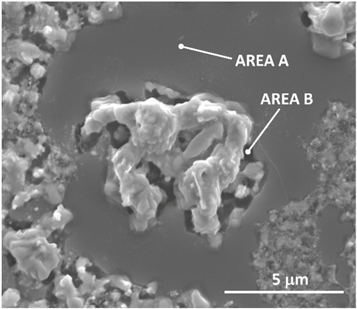
Figure 2. SEM image of the silicon substrate after the dewetting phase; the composition measured by EDX in points A and B is 100% Silicon.
Download figure:
Standard image High-resolution imageSEM/EDX measurements in correspondence of the aggregates have revealed a relatively high Si/Fe atomic ratio (ranging between 70.0 and 73.5 at% silicon), i. e. very close to the eutectic composition having melting point of 1220°C reported in the Fe-Si phase diagram [8]. The XRD pattern of the sample 1, measured after the dewetting, is consistent with these observations: the only crystalline phase present in the aggregates is constituted by tetragonal α-FeSi2 (figure 3).
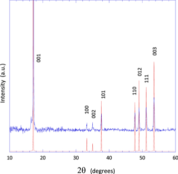
Figure 3. Blue line: XRD pattern of sample 1 after the dewetting; red line: reference α-FeSi2 pattern (ICSD—24360).
Download figure:
Standard image High-resolution imageFigure 4 reports the SEM images of samples 2–7, evidencing the effect of the progressive exposure of the substrate to the CO flux. Figures 4(A) and (B) reveal a situation similar to that of figure 1(B): no NWs are present after 30 s and 2 min exposure. The high density of NWs shown in figure 4(C) however indicates that after an induction time of about 3–4 min the growth of the NWs starts and proceeds very quickly. Then, for exposure times of 10 and 30 min a thick NW mat is observed (figures 4(D) and (E)).
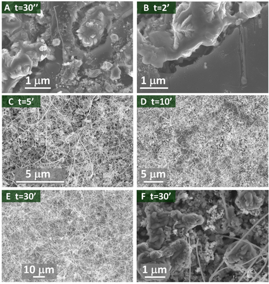
Figure 4. SEM images of the samples that were prepared with different time of introduction of CO.
Download figure:
Standard image High-resolution imageFigure 4(F) shows the morphology of the aggregates after the removal of the NWs by sonication. It can be noted a greater roughness compared to the images of figures 4(A) and (B), and the presence of some residual NWs that develop starting from the inside of the aggregates. The SEM/EDX point spectra acquired on these aggregates provide an average composition of 75 ± 1 at% silicon and 25 ± 1 at% iron, indicating that the composition of the aggregates does not change during the growth.
The morphology of the NWs has been studied in detail by means of TEM measurements (figure 5). Their total diameter is about 60 nm (figure 5(A)) with a 3C-SiC crystalline core having an average diameter of 20 nm and of an outer shell of amorphous silica (SiO2). The FFT spectrum reported in the inset of figure 5(A) allows to assess that the nanowire grows along a 〈111〉 direction. Some defects due to stacking faults of {111} SiC planes during the growth can be recognized (see the upper left corner of panel 5 A).

Figure 5. (A) TEM image of the cross section of a NW, (B) STEM-HAADF showing shape and size of the FeSi particle located at the NW tip. (C) HRTEM image and SAED pattern of the FeSi particle.
Download figure:
Standard image High-resolution imageFigure 5(B) shows the solidified droplet at the tip of the NW, whose diameter is indicatively twice the NW cross section. The SAED pattern of figure 5(C) reveals that it has a crystalline structure, consisting of the FeSi silicide phase (JCPDS 38-1397). This is in substantial agreement with the TEM/EDX analysis, that has revealed an average composition of 45 ± 2 at% Si and 55 ± 2 at% Fe.
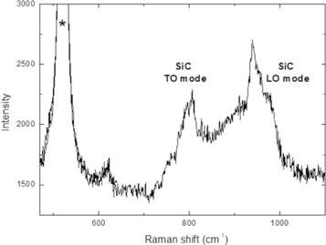
The NW core structure was confirmed by Raman spectroscopy, as reported in figure 6. The spectrum shows the characteristic peaks at 796 (transverse optical, TO mode) and 972 (longitudinal optical, LO mode) cm−1 which confirm the crystalline phase of 3C-SiC [9, 10].
Figure 6. Raman spectroscopy of the NW sample prepared with 30 min of introduction of CO. The peak indicated by * is due to the silicon substrate.
Download figure:
Standard image High-resolution image
3.1. Discussion: towards a mechanism
A plausible growth mechanism must be in agreement with the results of the experiments carried out. These can be summarized as follows:
- –the dewetting phase leads to the formation of aggregates whose main component is FeSi2;
- –the composition of the aggregates remains constant during the growth, only the morphology changes;
- –the growth of the NWs starts after a 3–4 min exposure to the CO flow and then proceeds very quickly;
- –the nucleation process occurs in correspondence of the aggregates;
- –the grown NWs present a rounded cap consisting of crystalline FeSi.
We have formulated a hypothesis based on a sequence of processes consistent with the experimental information.
The formation of the FeSi2 phase, by the way in semi-melted form, is still to be clarified, since not apparently consistent with the Fe-Si phase diagram. A tentative explanation can be as follows: first, Fe(NO3)3·9H2O decomposes to Fe2O3 at about 523 K [11]. In the adopted operating conditions (1100 °C and under N2 flux), it is presumable that Fe2O3 reduces to metallic iron in a three-stages process:

in this way, nanocrystalline Fe is formed: according to studies on the relationship between melting point and particle size [12, 13], it can be assumed that Fe nanoparticles have a significantly lower melting point than that of bulk Fe, and that this also entails a lowering of the melting temperature of the eutectic or in any case a modification of the phase diagram, without further excluding that the reactivity towards the Si substrate could be significantly increased. As a final result, metallic Fe reacts with Si yielding FeSi2 in liquid or semi-liquid form.
After the substrate is exposed to the CO flux, a VLS mechanism takes place. The FeSi2 droplets act as collector for the CO gas: an induction time of 3–4 min allows to achieve the supersaturation conditions necessary for the nucleation. Nucleation and growth take place at interface between collector and substrate. The involved reactions must account for formation of SiC as well as for the transformation of FeSi2 into FeSi, which certainly occurs in the collector. We have hypothesized the following processes:


In practice, CO diffuses through the droplets of FeSi2 (collector) and reacts forming SiC, which due to its high melting point precipitates at the interface giving rise to the core structure, and SiO gas, which reacts further with CO forming both SiC and SiO2, the former contributing to the core growth, the latter forming the amorphous shell on the core wall. Reaction (3) is often invoked as responsible for the formation of core–shell SiC-SiO2 NWs [14]. The SiO gaseous species can in fact form through different processes, that cannot be excluded even within the present growth system. Preliminary thermodynamic calculations indicate that reaction (2) is weakly exothermic (ΔrH ∼ 50 kJ mol−1) whereas reaction (3) is strongly exothermic (ΔrH ∼ 1000 kJ mol−1, [15]). There is therefore a release of heat and an increase in temperature in the collector: at the beginning of growth this leads to a further softening of the cap which favors the adsorption of CO and a general increase of the reaction rate, as experimentally observed. As the growth proceeds however, the Fe-Si system progressively evolves from FeSi2 to FeSi, whose melting point is significantly higher [8]. Once this composition is reached, the collector solidifies and the reaction (2) stops: subsequent small increases in the length of the NWs can be associated with the reaction (3), fed by gaseous SiO deriving from secondary processes. As a result, at the end of the growth a solidified droplet made up of crystalline FeSi remains on the tip of the NW.
4. Conclusions
Experiments of growth of SiC-SiO2 core–shell nanowires carried out by varying the exposure time to CO flow have provided useful information for understanding the growth mechanism. SEM measurements allowed to verify that the growth begins after 3–4 min of exposure to the CO flow and then proceeds very quickly. By means of EDX, XRD and TEM measurements it was possible to establish the composition of the promoter droplets at the beginning and end of the growth phase, and on this basis a nucleation and growth mechanism of NWs was proposed. Although consistent with the experimental observations, this mechanism does not answer all the still open questions, concerning e.g. the formation of FeSi2, the role of gaseous SiO in the development of NWs and the possible processes, currently denoted as secondary, from which it can originate. The results presented, as well as their interpretation, must be considered as a basis for discussion with the intention of obtaining useful data to improve the understanding of a complex process, or at least to give indications for further experimental work in this direction.
Acknowledgments
The authors are grateful to Mr Tullo Besagni for his support and useful discussions during the preparation of this paper.