

Abstract
Photovoltaic (PV) energy conversion of sunlight into electricity is now a well-established technology and a strong further expansion of PV will be seen in the future to answer the increasing demand for clean and renewable energy. Concentrator PV (CPV) employs optical elements to concentrate sunlight onto small solar cells, offering the possibility of replacing expensive solar cells with more economic optical elements, and higher device power conversion efficiencies. While CPV has mainly been explored for highly efficient single-crystalline and multi-junction solar cells, the combination of thin-film solar cells with the concentration approach opens up new horizons in CPV. Typical fabrication of thin-film solar cells can be modified for efficient, high-throughput and parallel production of organized arrays of micro solar cells. Their combination with microlens arrays promises to deliver micro-concentrator solar modules with a similar form factor to present day flat-panel PV. Such thin-film micro-concentrator PV modules would use significantly less semiconductor solar cell material (reducing the use of critical raw materials) and lead to a higher energy production (by means of concentrated sunlight), with the potential to lead to a lower levelized cost of electricity. This review article gives an overview of the present state-of-the-art in the fabrication of thin-film micro solar cells based on Cu(In,Ga)Se2 absorber materials and introduces optical concentration systems that can be combined to build the future thin-film micro-concentrator PV technology.
Export citation and abstract BibTeX RIS

Original content from this work may be used under the terms of the Creative Commons Attribution 3.0 licence. Any further distribution of this work must maintain attribution to the author(s) and the title of the work, journal citation and DOI.
1. Introduction
Concerns regarding the world's environmental sustainability and energy resource depletion have become increasingly evident, and there is an urgent need to mitigate and prevent these issues. The substitution of traditional energy sources by renewable ones is a pressing environmental challenge. For electricity supply, photovoltaic (PV) solar energy is being adopted at an accelerated pace because of its low financial generation costs, proven reliability and reduced associated carbon emissions. Strong research and development efforts are still being directed to decrease the price of solar electricity by reducing the cost of the PV module or by increasing the system light to electricity power conversion efficiency.
Concentrator photovoltaics (CPV) uses an optical system to collect solar irradiance and concentrate it on a smaller solar cell. This allows us to replace expensive or scarce materials used in the solar cell with much cheaper optical elements [1]. The optical system collects sunlight and concentrates it on the solar cell with a higher power density, which can in turn increase the efficiency of the solar cell. The ratio between the area of optical aperture to the area of the solar cell is called geometrical concentration (Cg, often indicated as its value followed by an X). Ideally, the reduction of solar cell area facilitates the use of more expensive, high-efficiency solar cells, leading to a higher energy yield and a lower levelized cost of electricity (LCOE) eventually being competitive with standard flat-plate PV technology. However, there are fundamental drawbacks linked to a CPV system; it cannot collect the diffuse fraction of sunlight and requires precise sun tracking. At high-concentration levels, temperature increase of the solar cell leads to decreased efficiency, an effect that can be mitigated by hybrid systems that use this excess thermal energy for thermal energy conversion [2, 3] or thermoelectric generation [4]. It has also been reported that at very high irradiance the relative efficiency decrease with temperature becomes weaker [5, 6]. A list of advantages and disadvantages of CPV is given in table 1.
Table 1. Advantages and disadvantages of traditional CPV.
| CPV advantages | CPV disadvantages |
|---|---|
| High-efficiency [7] due to a logarithmic increase of the open-circuit voltage with light intensity, according to equation (1) (see below) | Requires sun tracking |
| High energy output in locations with a high fraction of direct irradiance [8] | Cannot collect diffuse irradiation |
| Logarithmic decrease of the absolute value of the negative temperature coefficient of Voc with light intensity [5, 6] | Not suitable for rooftop applications |
| Low energy payback time and carbon emissions | Limited deployment—mainly in regions with high direct normal irradiation and for space-constrained or very high-efficiency applications |
| Less semiconductor material usage than flat-plate | Higher impact of soiling |
| Low capital expenditure for manufacturing, production facilities and infrastructure | Larger system cost per Wp than flat-plate PV |
| Maximum energy yield per land area | Maintenance (especially mechanical and electronics parts) |
| In some large-area CPV (e.g. parabolic dish), the active cooling systems needed to reduce temperature can be employed to generate thermal energy that can be used for water heating [2] | High operation temperatures decrease the power output or require the application of active cooling systems |
| High local content for local manufacturing, installation, operation and maintenance [2, 9, 10] | Too large variability of module architectures |
CPV has achieved very high efficiencies using four-junction solar cells made of III–V semiconductors: 46% for a solar cell under 508 suns of intensity [11], 43% for a single-lens concentrator [12] and 38.9% for a whole module with an aperture area of 812.3 cm2 [13]. However, due to the much smaller installed capacity and maturity of CPV systems, their price is still higher than that of flat-plate systems, with an estimated system cost between 1.4 and 2.2 €/Wp and an LCOE between 0.10 €/kWh and 0.15 €/kWh at locations with a high fraction of direct irradiance, around 2000 kWh m−2 per year [14].
1.1. CPV system and components
A CPV system has two essential elements: the optical collector and the receiver [9, 15]. The optical collector can be a mirror, lens or a combination of both [16] and the receiver consists of a solar cell with an optional secondary optical element (SOE), heat distributor and electrical contacts [9]. The collector and receiver are referred to as the concentrator module [9, 15]. A concentrator module is typically composed by
- An array of solar cells designed for operation under concentrated light, appropriately interconnected electrically. A concentrator cell with its means of interconnection is called the receiver.
- An optical system able to efficiently concentrate direct sunlight onto the solar cells with sufficient angular tolerance.
- A mechanical subsystem for aligning permanently solar cells and concentrator optics, protecting them from the environment (humidity, dust, water, hail, etc), providing electrical insulation and evacuating heat.
CPV modules are typically installed on a precise sun tracker to be aligned to direct sunlight. A collection of sun trackers or CPV arrays are interconnected to create a system and to feed an inverter. However, several concepts where the external tracker is substituted for some internal movement mechanism, or integrated tracking system, are currently in development [17]. These integrated tracking solutions will allow CPV to be integrated in fixed structures, providing access to the large rooftop market.
CPV systems can be classified according to their characteristics in several categories such as concentration ratio (low, medium, high), optical component (lenses or mirrors), optical shape (point-focus, linear focus, etc), solar cell type and material (single-junction, multi-junction, silicon, III–V semiconductors, thin films), cooling method (passive or active) and tracking method (single-axis, dual axis, stationary, quasi-stationary, etc) [2, 16, 18, 19]. With respect to the concentration factor, the CPV system is classified as low-concentration photovoltaics (LCPV) for concentration factor <100X and as high-concentration photovoltaics (HCPV) for concentration factors between 300–1000X. While LCPV are typically linear systems based on crystalline silicon solar cells and single or dual axes tracking, HPCV are based on point-focus collectors, multi-junction solar cells and dual-axis tracking [2, 9].
The concentration of sunlight and corresponding increase in the number of photons lead to a linear increase in the photocurrent proportional to the concentration factor (C). At the same time, an increase of the open-circuit voltage (Voc) due to a logarithmic dependence of the Voc on the photocurrent density (Jph) results in:

Here, A is the diode factor, kB the Boltzmann's constant, T the temperature, q the elementary charge and J0 the reverse saturation current density.
1.2. Motivation for thin-film micro-concentrators
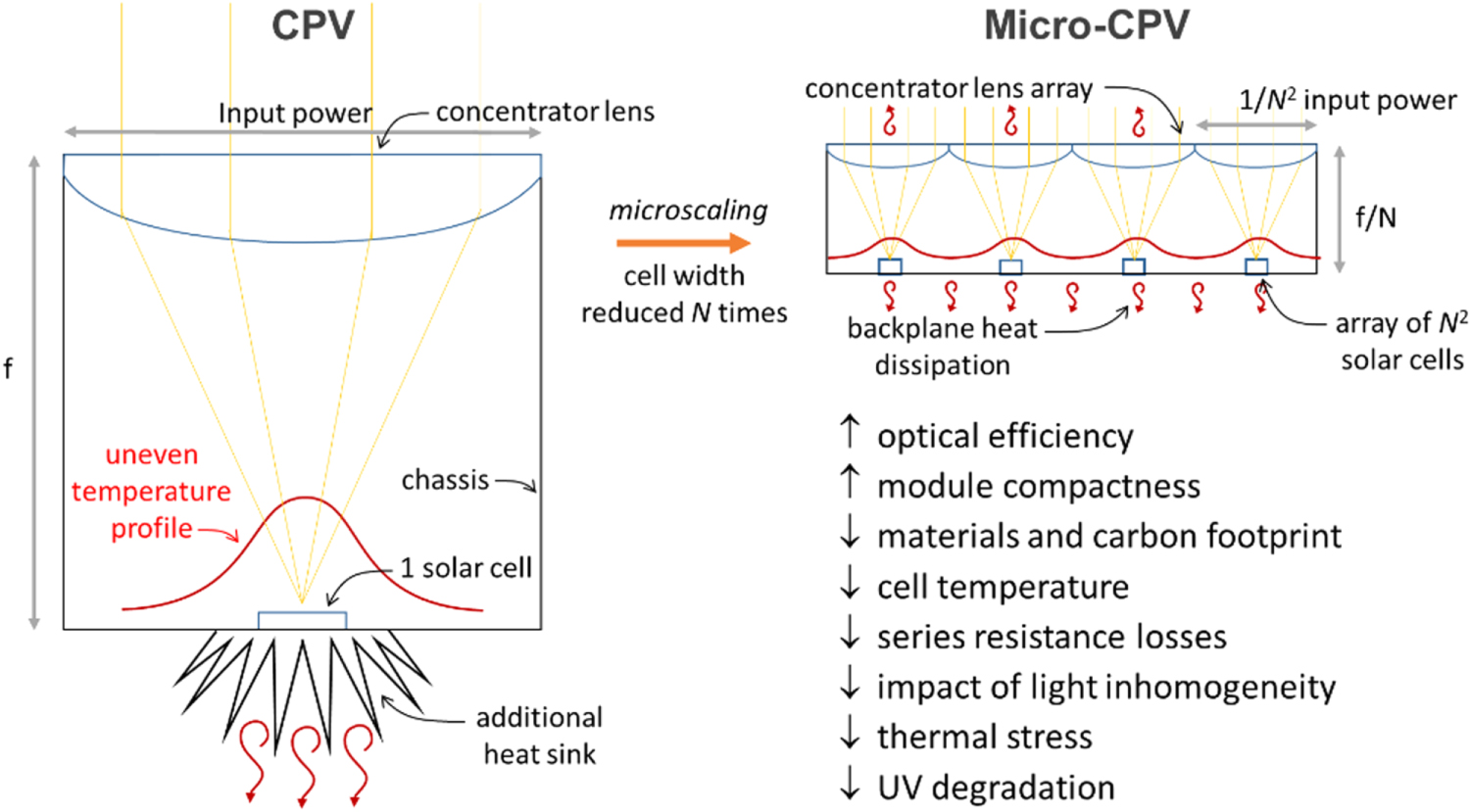
To decrease the costs of CPV, micro-scale concentrator photovoltaics (micro-CPV) (figure 1) have been proposed, where the solar cells are miniaturized to an area of less than 1 mm2 [9, 20]. By reducing the cell size to the sub-mm range, several benefits can be potentially achieved, such as materials savings, costs reduction, thermal management and enhanced efficiency [9, 20–22]. At the same time, the size dependence of efficiency of various types of solar cells can be different. For example, for III–V multi-junction cells, the decrease of the cell size from 1 cm to 1 mm was experimentally shown to result in an increase in efficiency and light intensity at which efficiency peaks [23]. However, this trend seems to asymptote for these devices at the cell dimension below 1 mm and certainly below 0.1 mm [24]. In addition, some manufacturing challenges related to the small size of the cells and the increased number of units to manipulate are expected [20].

Figure 1. Scheme illustrating the potential advantages of micro-scaling concentrator solar cells. On the left, a standard CPV system, where f is the focal distance. On the right, a micro-concentrator system with N2 miniaturized solar cells and respective increase (arrow up) or decrease (arrow down) of relevant characteristic parameters.
Download figure:
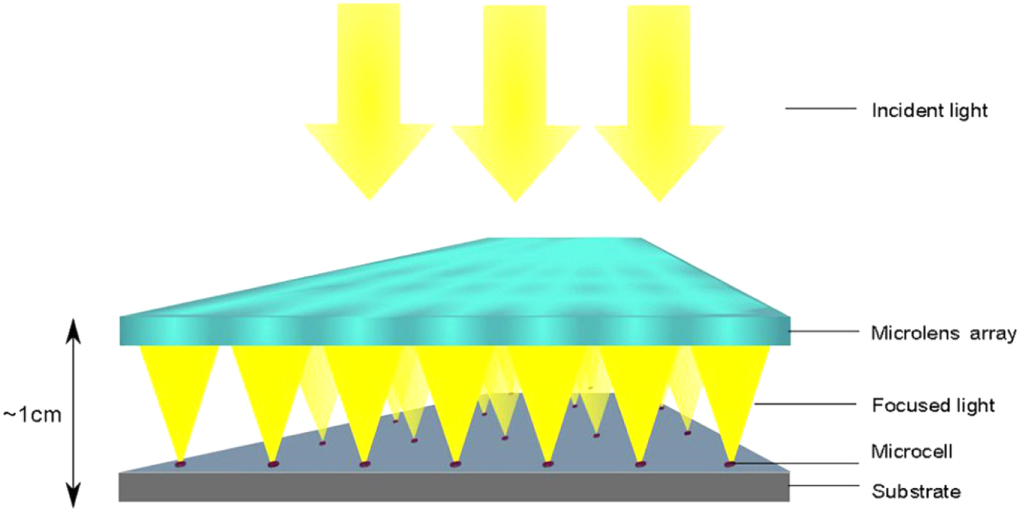
Standard image High-resolution imageOn the other hand, downscaling CPV to the micro-scale also opens new routes for thin-film solar cells. Thin-film solar cells already benefit from production processes with lower cost and higher savings in materials and energy demand. Therefore, by combining micro-CPV with thin-film solar cells, the cell area and consequently the used absorber material can be reduced by 1 to 2 orders of magnitude without power loss (figure 2) [25–27]. Thin-film technologies such as copper indium gallium diselenide (Cu(In,Ga)Se2—CIGSe), cadmium telluride (CdTe) and hybrid-perovskites are based on scarce and/or toxic elements. Thus, the reduction of the used material is imperative. The miniaturization allows the reduction of these materials, since under concentration only a fraction of the solar panel has to be covered by solar cells [28]. An overview of the benefits of thin-film micro-CPV, compared to conventional CPV and other technologies is given in table 2.

Figure 2. Schematic of a thin-film micro-concentrator PV device. This figure is reproduced from [25].
Download figure:
Standard image High-resolution imageTable 2. Advantages of thin-film micro-concentrator PV in comparison to regular CPV technology.
| Thin-film micro-CPV advantages | Regular CPV technology |
|---|---|
| Optical efficiency | Shorter optical paths lead to lower absorption losses. |
| Material consumption | The short focal length leads to thin modules that employ less material. Weight and volume are proportional to cell size. |
| Transportation and installation costs | Thinner modules can be more densely packed and transported and are easier to handle for installation. |
| Cell assembly costs | Highly parallel large-area thin-film solar cell processing can be used instead of individual pick and place of solar cells and lenses [29]. |
| Cell temperature | As the heat input per cell is reduced, solar cell temperature decreases. Furthermore, as the ratio of surface area to volume becomes higher, heat dissipation to ambient increases [27]. |
| Series resistance losses | The current generated at each cell is lower. Therefore, the series resistance losses can be reduced, taking advantage of the larger freedom in series/parallel interconnections [20]. |
| Lower impact of light spot inhomogeneity | Shorter current paths alleviate resistive losses due to local peak light intensity [22]. |
Among the different materials used for thin-film solar cells, copper indium gallium diselenide (Cu(In,Ga)Se2—CIGSe) has been intensively investigated and efficiencies up to 23.35% were achieved for 1-sun illumination [7]. The first steps for the miniaturization of CIGSe solar cells were taken by Tuttle et al [30], who reported 0.1 cm2 CIGSe solar cells for use in low-concentrator applications. They achieved a 14.8% efficiency at 1 sun and 17.7% at 22 suns, with a Voc increase from 614 to 713 mV. Ward et al [31] also reported 0.1 cm2 CIGSe solar cells, which were isolated by lithography and a 20 s dip in 10% HCl to remove the CdS and ZnO layers. Front contact grid lines of 10 μm width and 150 μm pitch were used and 21.5% efficiency was obtained at 14 suns using a flash solar simulator. Further increases in concentration did not lead to improved device performance. In 2014, Ward et al [32] realized 23.3% efficiency at 14.7 suns with a 0.1 cm2 device. Although these efficiencies were competitive or better than the respective one-sun efficiency records, these devices were still not yet truly micro in scale.
In recent years, CIGSe micro-concentrator solar cells have received increasing attention and several key results have already been achieved showing the viability of the CIGSe micro-concentrator concept. For example, CIGSe micro solar cells prepared by a top-down fabrication have shown an efficiency of 21.3% at a concentration of 475X [33]. For this proof-of-concept demonstration, a regular CIGSe solar cell was used, from which microcells with a diameter of 50 μm were defined by photolithography [33, 34]. On the other hand, bottom-up approaches have successfully demonstrated the material-efficient fabrication of CIGSe micro solar cells [26, 27, 35].
The miniaturization also influences the thermal management and resistance losses. Different to conventional CPV, which typically involves passive or active cooling, micro-CPV does not have this requirement. In a microcell the heat dissipation is better due to a higher surface-to-volume ratio, limiting the increase in cell temperature and consequently reducing thermal losses [20, 27]. Paire et al [34] demonstrated that for microcells under 50 μm in diameter the temperature increase is less than 20 K at 1000 suns (using a 532 nm laser source), confirmed by indirect measurement of the temperature by means of photoluminescence (PL). Sadewasser et al [27] showed by numerical simulations that for microcells smaller than 200 μm the temperature increase can be kept below 10 °C above the temperature of a flat-panel solar cell up to 100x concentration, evidencing that the temperature increase scales with the cell size.
Concerning the size effects on the resistive losses, a theoretical study from Paire et al analyzes the effects of micro-scaling CIGSe solar cells on the electrical performance of each cell [22]. Their model, based on the spread sheet resistance, proves that the resistive effect is less detrimental for smaller cells, resulting in higher fill factors (FFs). Thus, under concentrated light, the micro solar cell performance will not be limited by its resistive losses, as happens with planar absorbers [22]. This result was confirmed by the same group, when CIGSe cells with diameters from 15 to 150 μm were fabricated. The maximum efficiency was obtained at one magnitude higher concentration ratio compared to previously fabricated planar absorbers, proving that the sheet resistance becomes negligible at smaller sizes [34].
Although it has several benefits, micro-CPV also has challenges that need to be taken into consideration. Difficulties related to the micro-scale size are inherent in all processes, since accuracy is fundamental in the manufacture and connection of microcells and micro-optics. In addition, Dominguez et al described challenges such as the optical alignment in different stages with precision, the use of advanced materials and the integration of microsystems over larger areas [20].
In this review paper, we will describe the current state-of-the-art in the field of thin-film micro-concentrator solar cells and provide an outlook for the next steps in the development of this promising PV concept.
2. Device fabrication strategies
Over the last years, fabrication studies of CIGSe micro solar cells for concentrator PV have achieved significant results. Two different approaches are currently used for the microcells fabrication: top-down, where the microcells are defined by etching or shading of planar absorbers and, bottom-up, which aims at local absorber growth.
2.1. Top-down approaches
Top-down fabrication of micro solar cells was initially performed to provide proof-of-concept devices and explore the suitability of CIGSe micro solar cells for concentration applications, and study the properties and limitations of micro-scale CIGSe solar cell devices. Top-down fabrication refers to the fact that a large-area CIGSe absorber layer, or a full solar cell device are used and in a subsequent step a part of, or a whole micro solar cell is isolated for characterization. The fabrication techniques used follow different approaches from simple material removal by single-step scratching, to more complex multi-step photolithography processes leading to shadowing or realizing materials removal by etching. The fabrication methods for the top-down approaches are shown comparatively in figure 3, and the results of these different approaches are described in the following.

Figure 3. Different fabrication methods for defining micro solar cells by (a) applying an electrically insulating layer between the i-ZnO resistive layer and ZnO:Al window layer [34, 36–39], (b) etching away surrounding device stack [28, 37], (c) varying the P3 mechanical scribing position [40], (d) removing buffer and window layers using a laser or chemical etching [41] and (e) mechanical device stack scribing. Black and red triangles indicate position of front and back contact, respectively.
Download figure:
Standard image High-resolution imageIn 2011, Paire et al [36] realized a circular micro solar cell, where the Mo back contact, CIGSe absorber layer, CdS buffer layer and the i-ZnO are continuous large-area layers, but the ZnO:Al window layer is restricted to a 15 μm diameter by means of a SiO2 insulating dielectric layer (see figure 3(a)). The ZnO window is contacted at the periphery of the cell with a titanium/gold bilayer, ensuring that the cell is not shadowed by the electrical probes when contacted. For comparison, a 0.1 cm2 reference device completed in the regular way showed an efficiency of 13.2%, Jsc of 28.1 mAcm−2 and Voc of 631 mV under standard AM1.5 (air mass 1.5) illumination. The micro solar cells were tested using a 532 nm green laser. The Jsc increases linearly with laser power up to 2 × 10⁵ mWcm−2, which corresponds to an optical concentration factor of 2000X compared to AM1.5 conditions. For a concentration of 120X, a maximum efficiency of 17% was found, while for higher concentration the efficiency drops to its initial value at around 1250X (see figure 4). However, the Voc continues to increase nearly logarithmically with the short-circuit current, as predicted by equation (1). Nevertheless, the experimental Voc data do show a slight downward curvature as the concentration factor increases. The two likely main reasons for this behavior are the temperature sensitivity of the reverse saturation current density (J0) [42] and the product of the current and series resistance, both becoming more important at high-concentration factors. The maximum efficiency occurs when the Voc increase is matched by the corresponding voltage drop due to the resistive losses. This maximum occurs at ∼ten times higher concentration factors than for standard solar cells [32], showing that the micro design enables significantly lower TCO resistances, due to the low spreading resistance, and thus the series resistance is limited to other sources, which are independent of the size. In fact, the series resistance of the solar cell drops with increasing light flux, which the authors attribute to a reduction of the intrinsic series resistance of the absorber due to the increased number of photo-generated carriers.

Figure 4. Characteristics of a 15 μm diameter micro solar cell. Device efficiency is plotted versus Jsc or laser power density. Inset shows Voc as a function of Jsc. Lines are guides to the eye. Reprinted from [36], with the permission of AIP Publishing.
Download figure:
Standard image High-resolution imageThe same group also studied the impact of the micro solar cell size by varying the diameter between 7 and 150 μm [43]. As the cell diameter decreased, the maximum of the Voc increased to higher concentration factors, which was attributed to lower operating temperatures, resulting from an increased surface area-to-volume ratio allowing better heat removal. The cell temperature at 1000X was estimated to change from 310 to 345 K as the cell diameter increases from 15 to 150 μm. PL measurements were used to check the cell temperature, as the PL spectra are sensitive to temperature. It was confirmed that a 25 μm diameter solar cell was operating at 310 K, in line with the previous calculation. The efficient heat transport for micro solar cells was also confirmed by finite element modeling [21].
Micro solar cells fabricated in the same way (figure 3(a)) showed the current best power conversion efficiency of 21.3% at 475X concentration [33]. This efficiency record obtained for a single 50 μm diameter micro solar cell was based on a better performing CIGSe starting material, where the micro solar cell showed a 1-sun efficiency of 16.3%. For these micro solar cells, higher concentration factors could be achieved before the efficiency saturated. Interestingly, a decrease of the 1-sun Voc as a function of the cell diameter was observed for micro solar cells below 50 μm diameter, made from the same quality absorber layer. This drop was attributed to the 'mesa', presumably the walls of the micro solar cell, which would limit the minimum size of the micro solar cells, unless more resistive walls could be found.
Using a tunable white laser with 2 μm spot size, Lombez et al [38] reported external quantum efficiency spectra for a 25 μm diameter micro solar cell, fabricated as previously described (figure 3(a)), where the band gap varied only 10 meV from 1.17 to 1.18 eV within a single cell. However, the calculated carrier diffusion length changed from 1.2 to 1.8 μm, depending on the measurement position. No systematic influence of the lithography or contacting ring could be observed. Rather, the variations appear inherent to the continuous co-evaporated absorber layer that was used. PL spectra were also used to calculate the quasi-Fermi level splitting (QFLS) with 2 μm resolution, which is a measure of the maximum possible Voc achievable by the device [39]. An average QFLS of ∼800 meV was determined, while the lowest QFLS (about 15 meV lower) was observed around the perimeter of the micro solar cell. This drop only appears around the first pixel of measurement though, suggesting that detrimental edge recombination is limited to the first one or two grains of the CIGSe.
A different fabrication technique for top-down CIGSe micro solar cells was presented by Paire et al (figure 3(b)) [28, 37]. The fabrication of these mesa micro solar cells relies on a complete large-area CIGSe solar cell device, onto which a photoresist is deposited and patterned. Subsequently, the ZnO and CdS layers are removed with hydrochloric acid and the absorber layer is dissolved using a bromine-based etchant. The resulting mesa micro solar cells are free standing diodes where the edges of the active layers are in direct contact with air, but were presumably passivated by the chemical etch. Square-shaped micro solar cells with areas from 1 × 10⁻⁶ cm2 to 1 × 10⁻¹ cm2 (corresponding to side length between 10 and 3162 μm, respectively) with adapted contacts (figure 3(b) iii) were investigated to elucidate whether the Voc is affected by edge recombination. Voc was observed to be essentially constant until the area/perimeter ratio is less than 10 μm; for smaller area/perimeter ratios, edge recombination dominates over bulk recombination.
The effect of edge recombination was specifically addressed by comparing two different etching solutions for the CIGSe absorber, aqueous KBr/Br2 solution with a pH7, which avoids any further unnecessary etching of the already removed CdS and ZnO layers, and a combination of KBr/H2SO4/H2O2/KOH [28]. Here, the hydrogen peroxide is used to oxidize the bromine anions to Br2 in situ and the potassium hydroxide is used to increase the pH to around 7. These etchants do not etch the material vertically. Hence, depending on the conditions, CIGSe may slope out from under the CdS/ZnO top layers or it may be etched below the ZnO/CdS. After the etching, a layer of insulating epoxy polymer is deposited, leaving the top of the micro solar cells free. Subsequently, the cells are metalized and another layer of ZnO:Al is sputtered on top for electrical contacting purposes. For the CIGSe micro solar cells fabricated with the KBr/Br2 etch, no evidence of edge recombination was observed for devices down to 10−5 cm2, equivalent to a circular cell with a diameter of 36 μm. On the other hand, the hydrogen peroxide-based etchant was found to induce a high leakage current at low applied biases. The authors suggest that the Br2 solution leaves a stoichiometric stable surface, whilst the H2O2-containing solution does not. Different-sized diodes from 18–250 μm were tested under light concentration, showing that the maximum efficiency is lower for larger device areas due to the greater spreading resistance. Interestingly, the effect of shunt at low light concentration was removed nearly entirely below 20X concentration factor. In this study, a maximum Voc of 953 mV was achieved at 1650X for a 25 μm diameter cell, where the voltage was limited by a rise in device temperature. Light-beam-induced current (LBIC) measurements, 1 μm resolved, of such a mesa diode showed that current collection is uniform until 1 μm from the edge. Using a simple model, the authors estimated a minority carrier diffusion length of 0.9 μm and a surface recombination velocity of 1.3 × 10⁴ cms−1. Thus, the bromine-etched boundary of the device appears no worse for recombination than a normal grain boundary.
Reinhold et al [40] fabricated micro solar cells in line shape by employing the standard P1, P2 and P3 scribes used for interconnecting individual solar cells in a monolithic CIGSe module and placing a second P3 scribe at a distance of 200–1900 μm to the P1 scribe (figure 3(c)). The P1 scribe was made by a 1064 nm laser, and P2 and P3 were scribed mechanically. The cells were micro in the direction between the contacts, but with 11 mm length parallel to the contacts. For light concentration experiments, the devices were cut in length down to 3 mm. Improvements in efficiency were found for all sizes up to the range of 10–20X concentration factor. The best improvement was for the 500 μm wide device, achieving an absolute increase in efficiency of 3.8%–14.6% at 8X concentration. Above this concentration, the performance decreased due to losses in the FF, although the Voc continued to rise. The shunt resistance decreased by more than ten times under illumination from around 3000–150 ohm. In summary, it was concluded that the traditional P1–P3 scribe process needs to be re-evaluated in the context of micro solar cells, and that great care is required to achieve as high shunt resistance as possible, since small solar cells are disproportionately affected compared to larger ones.
Lotter et al [41] used state-of-the-art large-area high-performance absorber layers and formed micro solar cells with areas ranging from 4 × 10⁻⁴ cm2 to 1 × 10⁻² cm2 using two approaches. In a first attempt, micro solar cells were formed by mechanically scribing away the whole device stack from unwanted areas, which resulted in a low shunt resistance that scaled with the cell perimeter. The shunt issue was attributed to mechanical imperfections at the edges causing leakage paths in combination with the photoconductance of the CIGSe itself. Therefore, in a different approach, pulsed 532 nm laser scribing was used to only remove the ZnO, leaving the underlying CIGSe intact, which solved the shunting problem. However, a reduction in FF was observed, which was attributed to a defect positioned near the cell exterior walls due to the heating by the laser scribing. Finally, chemical etching of the CdS/ZnO using dilute hydrochloric acid was made using lithographic masking to protect the underlying microcells (figure 3(d)). Here, the value of the shunt resistance was also found to be dependent on illumination intensity, but overall it reduced less than for the devices made by mechanical scribing. Absorber layers with and without an alkali-fluoride post-deposition treatment (PDT) were compared for micro solar cells with approximately 5 × 10⁻⁴ cm2 area. The PDT sample started with a higher 1-sun efficiency around 19% compared to the 18.5% of the untreated one. However, under concentration it performed worse, reaching its maximum efficiency of ∼21.3% at 30 suns, while the untreated sample continued to improve in efficiency to 22.7% at 100 suns, the highest concentration factor measured. The authors found the series resistance of the absorber itself to be important, similar to Paire et al [36].
Lafont et al [44] similarly used large-area devices as a starting point to make micro solar cells by mechanically scribing away the CIGSe absorber. Micro solar cells with areas ranging from 6 × 10⁻⁴ to 25 × 10−4 cm2 exhibited a reduced shunt resistance by a factor of five compared to the large-area solar cell that they were made from. However, no dependence on cell area size or perimeter length was found, unlike in the case of Lotter et al [41]. Under 1-sun illumination, the short-circuit currents of all cells were similar, but the open-circuit voltages were slightly reduced. However, compared to the original cell the FFs were reduced by 10%–15%, presumably related to the poor shunt resistance. An LBIC line scan with low spatial resolution indicated that current collection was not significantly impaired at the edges of the device. Using a 4-point-probe configuration with 200 nm diameter tungsten tips, the authors measured a 2.1% efficiency increase going from 17.3% at 1 sun to 19.4% at 21X concentration factor for a mechanically scribed micro solar cell with an area 6 × 10⁻⁴ cm2.
In summary, the top-down device-making approaches have clearly shown that CIGSe is suitable for concentrated micro solar cell application, yielding the expected increase in device performance as the optical concentration increases. Furthermore, the increasing importance of the parallel and series resistances is highlighted compared to large-area cells.
2.2. Bottom-up approaches
Different to top-down approaches, bottom-up strategies allow the reduction of material consumption; specifically, the reduction of the content of critical raw materials is of fundamental importance to reach commercialization. Spatially controlling the growth of the micro absorber is the first requirement in the fabrication of ordered arrays of solar cells. To realize ordered patterns of the micro solar cells, several strategies for locally growing the absorber in defined areas are currently under study, by using masks, patterned or pre-structured substrates.
Two approaches using electrodeposition were reported nearly simultaneously [26, 27]. Sadewasser et al [27] employed a patterned insulating SiO2 layer deposited on top of the Mo back contact, leaving circular areas exposed, as shown schematically in figure 5(a). Depositing CuInSe2 into the micrometer-sized holes by electrodeposition, 5 × 5 arrays of micro solar cells (of 42 μm diameter) separated by SiO2 were fabricated. After the deposition, a selenization by thermal annealing in Se atmosphere was used to improve the material quality and crystallinity. To finish the solar cell, a standard CdS layer was deposited by chemical bath deposition and a ZnO double window layer was sputtered. Cross-section scanning electron microscopy (SEM) images are shown in figure 5(b). The test of the solar cells by concentrated illumination showed an increase of the JSC from 40 to 180 μA for 4.5X concentration, demonstrating the method's compatibility with the concentration technology. In a subsequent study using the same fabrication approach, a 1-sun efficiency for a 200 μm diameter micro solar cell of 4.8% was achieved [45]. The authors also presented a detailed study of the growth mechanism for the electrodeposition on the micro-sized Mo electrodes [45].
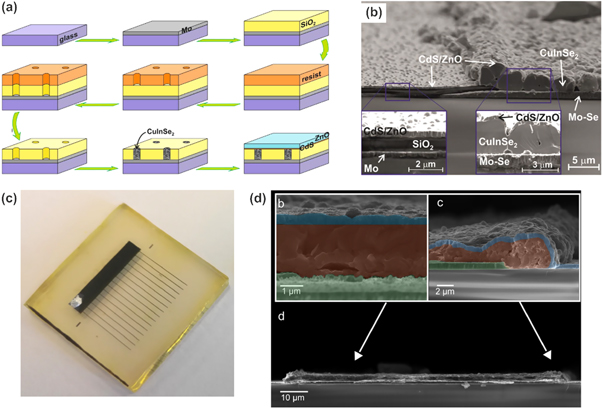
Figure 5. Bottom-up fabrication methods by electrodeposition of micro solar cell arrays. (a) Schematic of the fabrication sequence for a pre-structured back contact with conductive holes separated by an insulating matrix and (b) SEM cross-section of a CuInSe2 micro solar cell prepared by this method. Reprinted from [27], with permission from Elsevier. (c) CIGSe solar devices with micro-structured Mo back contact and (d) SEM images of the cross-section in the center and at the edge of the line-shaped micro solar cells. Reprinted from [26], with the permission of AIP Publishing.
Download figure:
Standard image High-resolution imageAt the same time, Duchatelet et al [26] fabricated CIGSe micro solar cells by electrodeposition on line-shaped micro-structured Mo back contacts with different patterns from 100 μm–0.1 cm, as shown in the optical image in figure 5(c). The Mo structuration was performed by standard UV lithography and etching, leaving conductive Mo stripes, onto which the CIGSe material is deposited by electrodeposition, forming homogenous layers. After the deposition, a standard selenization process was performed by annealing in a Se-enriched environment. Subsequently, a CdS layer was deposited by chemical bath deposition and ZnO/ZnO:Al bilayer was sputtered completing the solar cells. A SEM cross-section of the resulting devices is shown in figure 5(d). The devices achieved efficiencies up to 7.64% under 1 sun, proving that the patterning of the Mo contact is compatible with the formation of a high-quality absorber by electrodeposition.
These works demonstrated that selective growth of micro-scale Cu(In,Ga)Se2 by electrodeposition leads to functional solar cells.
Physical vapor deposition techniques (PVD) have also been proven to be compatible with the fabrication of micro absorbers. Heidmann et al were able to grow micrometer-sized indium islands by PVD [46]. A metallic indium precursor was deposited by PVD onto Mo substrates, which were pre-structured by femtosecond laser pulses [47, 48]. This site-selective modification of the Mo surface [49] promoted the localized deposition of In and thus created an easily tunable arrangement of nucleation sites [46–48], as schematized in figure 6(a). The In islands were subsequently coated by Cu and converted into CISe by a selenization process, after which excess Cu-Se was removed by a KCN etching step. To isolate the cells, a resist layer was spin coated, leaving the upper part of the CISe islands uncovered to be coated by the CdS buffer layer and transparent conductive oxide [46]. In a later work, CIGSe and CISe micro absorbers, such as the one shown in the SEM image in figure 6(b), were fabricated by this sequential PVD on laser-patterned Mo substrates, showing efficiencies up to 1.4% [50].

Figure 6. Bottom-up fabrication methods of micro solar cell arrays. (a) Schematic representation of pulsed laser contact structuration and (b) SEM image of a single CISe island grown by PVD on the structured substrate. (c) Schematics of the laser-induced forward transfer (LIFT) method and (d) optical micrograph of a single island deposited from a Cu-In donor layer. Reproduced from [51]. CC BY 4.0.
Download figure:
Standard image High-resolution imageAnother method for the fabrication of micro-CIGSe absorbers was presented by Ringleb et al [51]. Their approach uses LIFT, which consists of the transfer of a part of a donor film onto an acceptor substrate [52]. The method is schematically shown in figure 6(c). The main advantage of this method is the simplification of the whole fabrication process by reducing the number of steps in the micro-concentrator solar cell fabrication. The LIFT method was successfully implemented by Ringleb et al for CIGSe cells, transferring a metal precursor stack of Cu-In-Ga with thickness up to 1010 nm onto an acceptor Mo-coated glass substrate in a single transfer step, as shown in the optical micrograph image in figure 6(d) [51]. Subsequently, a standard selenization process in Se ambient, as well as an etching process by KCN to remove unwanted Cu-Se phases were performed. Solar cell devices were completed, as described before [46]. Although this approach has so far resulted in low efficiencies due to very limited JSC values, the photocurrent does increase as expected under concentrated illumination.
All the above-mentioned fabrication methods are summarized in table 3. All of the explored methods show promising results and further improvement and optimization is expected to lead to improved efficiencies in the future. Although the top-down approaches so far have led to higher efficiency values, the progress made with bottom-up methods has led to increasing efficiencies during recent years for similar micro solar cell sizes. When tested under concentrated illumination, they perform as their planar absorber competitors, evidencing the promising nature of the combination of micro solar cells and the concentrator technology.
Table 3. Overview of different approaches for the fabrication of CIGSe micro solar cells using material-efficient bottom-up methods.
| Fabrication method | Material | Size of individual micro solar cells (μm) | Efficiency under 1 sun (%) | Efficiency under concentrated illumination | Comments | References |
|---|---|---|---|---|---|---|
| Area-selective electrodeposition | CuInSe2 | 200 | 0.26 | No | Patterned SiO2 layer on top of Mo back contact, concentration by power variation of red laser | [27] |
| Cu(In,Ga)Se2 | 10–500 | 2 | 4.6% (35X) | Patterned SiO2 layer on top of Mo back contact, concentration by power variation of red laser | [45] | |
| Cu(In,Ga)Se2 | 1000 | 7.64 | No | Patterned Mo back contact, line-shaped cells | [26] | |
| CuInSe2 | 105 | 5.38 | No | Patterned Mo back contact, line-shaped cells | [26] | |
| Cu(In,Ga)Se2 | 200 | 4.8 | No | Patterned SiO2 layer on top of Mo back contact | [45] | |
| LIFT | Cu(In,Ga)Se2 | 50–100 | 0.15 | 0.237% (20X) | No prepatterning of the substrate. Transfer of the donor film in a spatially structured manner. | [51] |
| Area-selective PVD | CuInSe2 | 50–100 | 1.4 | 3.36% (20X) | Glass patterned by fs-laser, PVD Mo layer | [51] |
| CuInSe2 | 50–100 | 2.9 | 3.06% (3X) | Glass patterned by fs-laser, PVD Mo layer | [51] | |
| PVD | CISe | 60 | 2.9 | 3.1% (3X) | No prepatterning of the substrate, growth of indium islands | [46] |
Furthermore, other well-known thin-film deposition techniques might be employed favorably for the realization of micro solar cells maintaining the material-savings aspect. Among these other methods, the inkjet printing method has been successfully applied to the growth of planar CIGSe absorbers [53, 54] and could be extended for micro solar cell fabrication, as it allows a high spatial control of the film deposition. Similarly, aerosol jet printing and screen printing could be used for depositing the CIGSe and CISe precursors in a spatially controlled way [55].
To summarize the efficiencies for micro solar cells and micro solar cells under concentration achieved so far, figure 7(a) shows the efficiency values as a function of cell area. The VOC values are represented in figure 7(b). As seen already from the previous sections, although the top-down (green symbols) approaches have led so far to higher efficiency values, micro solar cells based on bottom-up methods (blue symbols) have shown increasing efficiencies during recent years for similar sizes. This difference is due to the better absorber quality obtained for top-down fabrication methods, which build on high-quality absorber material deposited by well-established and optimized deposition techniques, and which already show high 1-sun efficiencies. On the other hand, bottom-up fabrication of CISe and CIGSe micro solar cells is a very recent development and further experience and optimization of the growth methods is required before similar efficiency values can be obtained.

Figure 7. (a) Efficiency and (b) Voc values under 1 sun and upon illumination of micro solar cells fabricated by bottom-up (blue symbols) and top-down (green symbols) approaches. (c) Efficiency gain and (d) VOC gain for bottom-up (blue) and top-down (green) approaches upon concentration and expected values under concentration for the record efficiency CIGSe thin-film solar cell from [56] (dashed lines). Inset in (c) shows the difference Δ between experimental efficiency and the expected one. Data taken from (α) [36], (β) [28], (γ) [33], (δ) [44], (ε) [40], (η) [26], (θ) [27], (κ) [51], (λ) [57] and (μ) [46].
Download figure:
Standard image High-resolution imageNevertheless, the absolute gain in efficiency and Voc values as a function of concentration factor is actually developing in a similar way for both top-down and bottom-up fabrication methods, as shown in figures 7(c) and (d), respectively. The black dashed lines illustrate the expected efficiency and Voc gains upon concentrated illumination, according to equation (1) and assuming constant cell temperature and the values of JSC and FF obtained for the current record efficiency CIGSe solar cell [56]. The difference between the experimental values and this expected efficiency gain (inset) shows similar values for both approaches, evidencing the promising nature of the bottom-up approaches. Similarly, although the Voc gains found for top-down approaches are larger (figure 7(d)), the tendency shown by the bottom-up approaches seems very promising.
2.3. CIGSe micro solar cells with integrated concentration optics
Although microsystems that integrate concentration optical arrays with micro diameter solar cells have been applied to multi-junction solar cells [58, 59], up to now, only very little work has been presented on integrated CIGSe micro-concentrator solar cells with a dedicated optical system [29, 60] integrated with a microlens array with CIGSe micro solar cells fabricated by the top-down approach described above [28]. A prototype consisting of a combination of primary lenses and secondary optics was fabricated. The microlens array was manufactured from a cylinder array fabricated by photolithography that subsequently went through a reflow melting step, resulting in spherical-shaped lenses. The secondary lenses were fabricated by spin coating a resist on the microcell array, which was then covered with a spacer layer. After the alignment of the micro lenses with the microcells, another thermal reflow is done resulting in an array of 2500 smooth spherical micro lenses. The primary lenses are then fabricated by depositing a resist layer and a similar reflow process. Thus, the resultant micro-CPV module prototype consisted of an array of 2500 microcells of 54 μm each on a surface of 3 × 3 cm2 connected in parallel with an array of 2500 secondary micro lenses. Another array of 2500 primary micro lenses on a glass substrate was fabricated and stacked, in order to achieve a lens aperture area of 4.8 cm2. Surprisingly, the results of the system with only the secondary lenses shows a concentration factor higher than the theoretical value, indicating a probable waveguide effect resulting in extra light onto the microcells increasing the concentration factor. Current–voltage curves of the reference array, the reference array with secondary lenses and the complete system were measured. The complete system shows a 1.8% absolute efficiency increase to 12.6% at a concentration factor of 71.8X, which is ∼2% lower than the theoretical concentration factor of the microlens array. It is noteworthy that the FF decreases by 7% upon the integration with the primary lenses, due to an increase in series resistance.
3. Concentrator optics for thin-film solar cells
The aim of concentrator optics is to collect and concentrate sunlight onto a solar cell to increase its efficiency and reduce expensive or scarce semiconductor consumption. CPV systems can be classified in many ways according to the characteristics of the optical system. The preferred optical design will be mostly linked to the electrical characteristics, size and cost of the specific solar cell technology to be used as the receiver, which imposes the main design constraints and trade-offs. The optical architecture determines the Sun tracking strategy as well (single- or double-axis tracking, external or module integrated, etc).
3.1. Characteristics of concentrator optics
Concentrators introduce the need for additional figures of merit to understand and compare their performance. Optical efficiency is the ratio of the light power put on the solar cell to the light power at the optical aperture. Direct normal irradiance times the optics area is usually taken as the input power, as most concentrators have a very limited angular aperture. State-of-the-art efficiencies range between 80% and 90% for sunlight [61]. The optical efficiency given as a function of the wavelength is called spectral transmittance, which will not be constant because reflectivity, refractive index and absorption of materials depend strongly on wavelength. The global optical efficiency is then given by the integral over wavelength λ of the spectral transmittance T(λ) times the spectral irradiance of the incident light E(λ). Thus, it is strongly dependent on the incident light spectrum. A reference spectrum (typically AM1.5D) has to be used to allow reproducibility and fair comparison between different optical systems.

Geometrical concentration (Cg) is the ratio of optical aperture to solar cell area, usually indicated as the concentration value followed by letter 'X'. Increasing the concentration factor leads to a reduction of semiconductor material, but also reduces the field of view or angular tolerance of the concentrator. This fundamental relationship is described by the conservation of the etendue theorem, which for 3D concentrators is given by:

where Alens and Acell are the areas of the optical aperture and the solar cell, respectively, α and β are the angular extent of the input and output light beams, respectively, and nin and ncell are the refractive indices surrounding the entrance of the concentrator and the solar cell, respectively (figure 8). The angle α is described as the angular tolerance of the concentrator. This expression leads to maximum concentration achievable Cg,max:

If the concentrator casts a wide angle on the cell (65°), the maximum angular tolerance achievable for an 800X concentrator is ±2.75° (ten times the angular extent of the Sun). However, practical concentrators of that size have a much lower angular acceptance, in the range of 0.4°–1°, although some sophisticated designs may reach much higher levels.

Figure 8. Geometrical characteristics of a concentrator solar cell: lens aperture area Alens of the solar cell with area Acell and focal distance f.
Download figure:
Standard image High-resolution imageFrom a practical point of view, angular tolerance is given through the angle of acceptance. Acceptance angle is defined as the maximum tolerable misalignment with respect to the Sun for which the optical efficiency is still larger than 90% of the maximum. The parameter concentration-acceptance product (CAP) represents the tradeoff between high-concentration and high acceptance angle, how close a real concentrator is to being ideal:

Because the optical efficiency is always lower than 100%, the geometrical concentration of the concentrator does not define the actual power density on the cell. Thus, concentration ratio is defined as the light power density on the cell divided by the power density at the optical aperture, and is often designated by 'X'. In practical terms, it is usually taken as the ratio of the solar cell's photocurrent under the concentrator when exposed to direct sunlight, to the photocurrent of the bare cell under the same direct light. Short-circuit current is often used as a probe of photocurrent, although large resistance losses may introduce a significant deviation between both. If the concentration ratio is known, the irradiance on the solar cell can be estimated as the product of the direct normal irradiance available times the concentration ratio.
The spatial distribution of the concentrated light is another important characteristic because non-uniform illumination increases the series resistance losses of the solar cell [62]. The actual loss will depend strongly on cell technology, and it will vary with cell design parameters such as size, emitter thickness or the layout and thickness of cell contacts [36]. A peak-to-average ratio is a typical figure of merit, defined as the ratio of the peak irradiance to the average over the whole cell [63]. Peak-to-valley ratio is another useful related figure.
As most concentrator optics can be said to create a certain focus (output surface), a relevant figure is the focal distance (f) between the light-aperture plane and the focal plane where the solar cell is located, which roughly defines the minimum CPV module thickness and therefore its minimization is desired. However, optical efficiency greatly depends on the aspect ratio or f-number of the concentrator optic (f/#), i.e. the ratio between focal distance and lens aperture diameter (D):

When a simple aspheric refractive lens is considered (for instance a Fresnel lens), the optimal f-number is mainly a tradeoff between dispersion (the variation of refractive index with wavelength) and angular acceptance (see Optical losses below). Reducing f/# increases Fresnel losses, chromatic aberration and lens thickness, while increasing aspect ratio reduces the angular spread over the cell and hence the achievable CAP.
3.1.1. Optical losses
Theoretical optical efficiency calculated by design will not be achieved for a large variety of reasons. There are mainly four types of sources of loss: (i) light absorption through the optical path within transparent materials, whose absorbance cannot be zero, or imperfect reflection in mirrors (15% losses in aluminum mirrors and 5% losses in silver mirrors are typical). (ii) Fresnel reflection losses, which are found in every interface between two media with different refractive indices. This loss grows with the mismatch between indices and with incidence angle. Thus, faster lenses (more compact, lower f-number) suffer from larger Fresnel reflection losses. Anti-reflective coatings reduce this loss by adding a matching intermediate refractive index between the air and a high-index material. (iii) A group of losses is driven by dispersion, or the variation of refractive index with wavelength, i.e. optics behave differently for different spectral bands. Optics are designed typically assuming the refractive index of some reference wavelength (e.g. 550 nm), but most light will encounter lower or higher indices. This dispersion is responsible for chromatic aberration, where a lens creates different foci for different spectral regions. In practice, this effect enlarges the size of the concentrated spot, reducing the achievable CAP. (iv) Geometrical errors are another group of losses: surface roughness of a lens or a mirror produces scattering of the light, which in the case of concentrator systems will be mostly lost; form errors that deviate rays from the designed trajectory are originated by real-world fabrication errors (such as draft angle or tip rounding in Fresnel lenses, limited by molding processes) or deformations introduced under real operation (such as the deformation of silicon-on-glass lenses due to the mismatch in the coefficient of thermal expansion of both materials); a poor alignment between parts will have also an important impact on light rays lost and creates a mismatch especially between the optics of an array, typically originated by imperfect manufacturing processes at the module level.
3.2. Types of concentrators
3.2.1. Geometrical concentration
Concentrators can be classified according to their geometrical concentration. Low-concentration optics (Cg < 10x) are static or quasi-stationary concentrators with a wide angular tolerance, able to collect a large fraction of the diffuse irradiance. They are especially suited for integration on fixed planes such as in building integration [64, 65] or electric vehicle car roofs [66], typically using inexpensive solar cells.
Medium concentration is achieved for Cg between 10x and 100x. Both 2D and 3D shapes can be used to design the primary optic. However, reflective linear troughs similar to those used in thermal solar systems are the most typical system. This type of system can use single-axis tracking, optionally with some seasonal tilt [67, 68].
Finally, Cg > 100x is considered high-concentration. It results in a low angular tolerance, in the range of tenths of 1°, so precise tracking of direct sunlight is required. High concentration leads to maximum material saving and theoretical efficiency increase, but there will be a practical ceiling due to the tradeoff with the robustness and series resistance losses of a solar cell under highly concentrated light flux. Furthermore, high-accuracy tracking increases system cost. Record PV conversion efficiencies have been obtained using this configuration [12, 13].
3.2.2. Optical principle for light collection
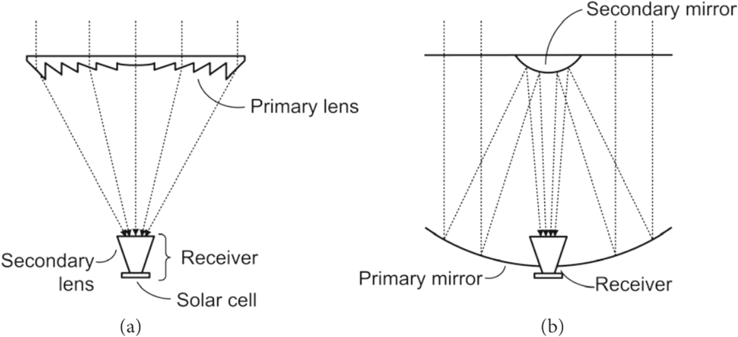
CPV optics must bend the trajectories of light rays to produce concentration on the solar cell. Most concentrators are based on refraction or reflection to collect and bend light on the solar cell. The vast majority of CPV installed capacity is based on a refractive lens as the primary optical element (POE), typically a Fresnel lens made of plastics such as PMMA or silicone-on-glass [69]. An SOE is often proposed, either refractive or reflective (figure 9). Reflection can be metallic or by total internal reflection (TIR). The integration of SOE and solar cell is known as the receiver.

Figure 9. Illustration of the two main optical architectures used in point-focus concentrators: (a) refractive or (b) reflective primary optic. Optical train often uses a final stage to increase concentration or angular tolerance, again either refractive or reflective.
Download figure:
Standard image High-resolution imageThere are other light-redirection mechanisms that have been used to concentrate light. Materials such as semiconductor quantum dots, rare earth materials and organic dyes can be dispersed in a transparent plate to create a luminescent solar concentrator (LSC). Incident light is absorbed by the dye and then re-emitted at a different spectral region, so it is not reabsorbed. The light is trapped by TIR and conducted towards the edge surfaces where it is coupled to a solar cell [70]. Since the edge area is smaller than the optical aperture, this approach allows for static concentration. However, optical efficiency of real luminescent concentrators is strongly limited by a number of loss mechanisms: reemission that escapes TIR, inadequate absorption bandwidth, re-absorption losses due to overlap of absorption and emission spectra, absorption by the matrix material (often PMMA) due to the long optical path, non-perfect fluorescence quantum yield and poor outdoor durability [71]. Still, tandem or cascaded LSC have reached a global electrical efficiency of 7.1% [72, 73].
Scattering and diffraction have also been used to produce waveguide coupling. The diffraction of gratings [74] and holograms [75] has been demonstrated to redirect light within a light pipe. However, optical efficiency for broadband sunlight is low due to the strong spectral selectivity of diffractive optics. Holographic solar concentrators have achieved 9% efficiency for 23% GaAs solar cells [76]. Scattering at the focal plane of concentrator lenses has been used for the same purpose [77].
3.2.3. Shape or symmetry of the optics
Most high-concentration systems are point-focus, i.e. an array of 3D designs produce concentrated spots on the solar cells, often the image of the light source (the Sun). There are exceptions to this rule; a 2D linear shape and single-axis tracking concentrates light 300X [78]. 3D concentrators are subject to the etendue conservation limit, as expressed above, but 2D concentrators have a much lower limit for the maximum concentration achievable:


3.2.4. Number of optical stages
Most CPV systems use one or two optical stages (POE only or POE plus SOE, respectively), but more stages are possible. The purposes of a SOE are manifold: increase the optical efficiency by collecting lost rays or better coupling light to the cell, widen the angular tolerance of the optical train for a fixed geometrical concentration, increase the concentration ratio, homogenize the light cast by the POE or protect the cell from the environment.
3.2.5. Solar tracking approach
Due to their limited angular acceptance, concentrators have to use rotation axes to point the optical system towards the Sun with the precision required. This is typically carried out using an external mechanical structure on which the CPV modules are mounted (Sun tracker). Low- to medium-concentration systems may allow the use of a single-axis (typically east-west tracking), but high-concentration systems require two high-precision rotation axes, which increases system cost significantly. Tracking structures account for more than 20% of the system cost [79]. Alternatively, integrated tracking concepts dynamically modify the optical system to steer the concentrated light towards the solar cells. Two main approaches are usually taken: beam steering or micro-tracking [80]. In beam steering, the light is redirected towards the axis of a fixed concentrator using a moving deflecting element. Systems using mirrors [81] or rotating prisms [81–83] have been proposed. Electrowetting has also been demonstrated to control a liquid prism for this purpose. On the other hand, the micro-tracking approach modifies the internal alignment between the optics and the receiver cell to track the movement of the solar angle. Either the optics or the cell can be moved to place the moving concentrated spot on the cell. Lateral displacement of the cell is a natural choice [84], but the foci of a simple aspheric lens for different incidence angles move across a curved path (Petzval curvature field), which complicates the mechanism of actuation. A radially-symmetric bi-convex freeform lens has been proposed to flatten the Petzval curvature [85]; its realization has demonstrated an optical efficiency higher than 80% for incidence angles up to 40° and a concentration ratio of 180X. Insolight has recently demonstrated this concept for pre-industrial modules, achieving peak 29% electrical efficiency. Another approach based on lateral displacement of two stages of plano-convex lenses designed using the simultaneous multiple surface (SMS) algorithm can theoretically achieve 500X with ±24° acceptance using a polar single-axis tracker [86–89]. Related to this concept, planar micro-tracking concepts use concentrator lenses to focus light on some micro coupling features that scatter or reflect light into a waveguide, which direct light towards the edges where the receiver cells are located. The couplers have to be displaced to compensate the movement of the focal spot. For this purpose, either the waveguides are laterally displaced or the coupler is made of some reactive material that varies its geometrical or optical properties when illuminated (heated) to produce appropriate redirection of the light [77, 90]. Planar micro-tracking employing a movable cell between two optical stages (a lens and a mirror) has demonstrated 30% conversion efficiency and the ability to generate 50% more energy than a 17%-efficient commercial silicon cell through side-by-side comparison [17].
3.3. Design considerations
The design of a concentrator is aimed at maximizing electrical efficiency and saving expensive or scarce materials, with the eventual goal of producing the lowest cost of generated electricity possible. However, there are a myriad of design parameters that will influence each other and are linked by fundamental trade-offs, so the design process involves taking some global decisions on the concentrator architecture a priori [91].
Typically, spot shape, geometrical concentration and cell size are chosen in the first place, and then the best optical architecture (refractive or reflective, single or two stage...) is chosen to maximize system efficiency and minimize cost. It is usual that a concentrator is designed to optimize the performance and lower the cost of generating electricity with a specific solar cell technology. Thus, the cell used determines the techno-economic constraints and relevant merit functions for the design. For instance, electrodeposition of CIGSe onto line-shaped Mo electrodes leads to line-shaped CIGSe micro solar cells [26], which then require an array of linear concentrators (2D shape with linear symmetry) to illuminate them (figure 10). Microcells have also been grown locally in a circular shape [27], which requires an array of point-focus concentrators (3D shape). Thus, the attainable concentration is much higher.

Figure 10. Illustration of (a) line-shaped and (b) island-shaped micro solar cells. Reprinted from [21], with permission from Elsevier.
Download figure:
Standard image High-resolution image
Optical design is driven by the techniques developed for non-imaging optics, where the transfer of energy has to be maximized regardless of image preservation. The most classic optical design procedure uses the edge-ray principle, where the concentrator refractive surface is designed for an extreme ray that defines the angular tolerance of the system using Fermat's principle (optical path preservation). The optical design assumes some particular wavelength, but dispersion of materials prevents most light from following this representative path. Therefore, a median wavelength has to be chosen for this design (typically ∼600 nm). However, more advanced techniques can be used such as the flow-line method or the SMS algorithm [92].
In view of the optical losses described above, there are many different requirements to optical materials. However, they can be summarized in high transparency (90% overall is a typical threshold) or reflectivity (95% of silver), proven durability (especially with regard to solar ultraviolet doses at the primary-lens stage or concentrated UV and heat at a secondary lens, which is a much more restrictive requirement) and low surface roughness to reduce scattering. Most common transparent materials are plastics (PMMA, PET, PC), PDMS, sol–gel or glass. Glass is typically used as a flat layer, but can also be shaped as a secondary lens using grinding and polishing of BK7-like materials in the case of flat surfaces (such as in a light pipe), or using molding with B270-like glass beads.
4. Conclusion and outlook
In this review article, we presented a concise overview of the current state-of-the-art in the field of Cu(In,Ga)Se2 thin-film micro-concentrator solar cells. Major achievements in the fabrication of CIGSe micro solar cells have been realized in recent years. Top-down fabrication of CIGSe micro solar cells from large-area deposited high-quality CIGSe material has led to efficiency values above 21.3% for 475X concentrated illumination, demonstrating the suitability of CIGSe for micro-concentrator PV applications. Several fabrication routes for the material-efficient and highly parallel fabrication of CIGSe micro solar cells have been shown, currently still leading to lower efficiency values. However, further research effort will certainly improve efficiencies and make these material-efficient approaches competitive. At present, the combination of a lens array with a CIGSe micro solar cell array of 625 cells on an area of 2.25 mm2 has led to an efficiency of 12.6% for a geometrical concentration factor of ∼73X. The fast development of CIGSe thin-film micro-concentrator PV will likely result in strong improvements of the technology in the near future. The main challenges at present are the development of material-efficient approaches for the fabrication of CIGSe micro solar cells with competitive performance, the development of suitable optical systems for the concentration of sunlight with a low geometrical footprint, such that the benefits of micro-concentrator PV can be fully exploited, and finally the combination of the PV and optical elements in an effective way.
Acknowledgments
We acknowledge support by the Micro-concentrator thin-film solar cells project (028922), co-funded by FCT and the ERDF through COMPETE2020. The work of C Domínguez is supported by the Spanish Ministerio de Economía y Competitividad (MINECO) and Fondo Europeo de Desarrollo Regional (FEDER) under the project MICRO-PV reference ENE2017-87825-C2-1-R.