

Abstract
Integrated electro-optic (EO) modulators are one of the building blocks of photonic integrated circuits. Here, we design and fabricate an EO Mach–Zehnder waveguide modulator on lithium niobate on insulator using photolithography assisted chemo-mechanical etching technology. We optimize the performance of multi-mode interferometer which serves as the 3 dB splitter as well as that of the inverse taper to achieve efficient fiber-waveguide coupling, resulting in a fiber-to-fiber insert loss of 7.6 dB for the fabricated device, with a half wave voltage (HWV) (Vπ) of 0.84 V and a HWV-length product (Vπ × L) of 3.4 V cm. The all-optical-lithography fabrication approach holds the promising potential for mass production of EO modulators of cost-effectiveness and low Vπ.
Export citation and abstract BibTeX RIS

Original content from this work may be used under the terms of the Creative Commons Attribution 4.0 license. Any further distribution of this work must maintain attribution to the author(s) and the title of the work, journal citation and DOI.
1. Introduction
Electro-optic (EO) modulators of low-power consumption, high bandwidth and low cost are nowadays ubiquitously used in optical information processing, optical sensing, precision measurement, etc [1–4]. Lithium niobate (LN) has excellent EO coefficient and optical transparency, which makes it as an attractive candidate to serve as the material platform for high performance EO modulators [5–8]. The traditional LN-based waveguide modulators are usually fabricated on the bulk LN crystal by ion diffusion and exchange. The relatively large mode size in the ion implanted waveguides give rise to high half-wave voltages (HWVs) and large footprints of the device, making it difficult to achieve high EO tuning efficiency and dense photonic integration [9, 10]. Recently, the advent of the thin-film LN platform (i.e. LN on insulator, LNOI) has provided the opportunity to produce LN waveguides of low loss, tight mode confinement, and small bend radius. Over the past a few years, the outstanding characteristics of the LNOI photonics have attracted much attention for constructing integrated EO modulators on LNOI [9–18]. These EO modulators are mostly fabricated using electron beam lithography (EBL) for the patterning of the mask followed by ion dry etching. The EBL allows to achieve high fabrication accuracy, whereas the production throughput is yet to be improved to meet the industrial standard [15, 19].
Meanwhile, ultra-low loss micro- and nano-photonic devices can be realized by femtosecond photolithography assisted chemo-mechanical etching (PLACE) technology [20, 21], such as the microresonator with quality up to 108 [22], and the waveguides with the loss as low as 0.027 dB cm−1 [21]. Moreover, the PLACE technology can have a competitive fabrication efficiency as well as large device footprint leveraged by high average power femtosecond laser and high-speed large-motion-range position stages, both of which are highly in demand by photonic industry [23, 24]. To showcase these, an all-optical PLACE scheme is proposed to fabricate the EO modulators on LNOI. Specifically, we characterize the performance of key components in the LNOI modulator including the multi-mode interferometer (MMI) for beam splitting and the waveguide taper for efficient waveguide-fiber interfacing. The static EO performance and the EO bandwidth (S21 parameter) are also measured. The demonstrated EO modulator features an overall fiber-to-fiber insert loss of ∼7.6 dB.
2. Device design and simulation results
The design of the EO modulator is shown in figure 1(a), in which light is coupled into LN waveguide using polarization-maintaining fiber (PMF, Corning Incorporated PM-HA13-PS-U25D) mediated by inverse taper edge couplers. In our design, the modulator is driven in a push–pull configuration, and the arm lengths of the EO modulator are chosen to be 4 cm aiming at low Vπ . The total length of the EO modulator device is 5 cm. The cross-sectional geometry of the EO modulator arms and the Cr–Au electrodes is shown in figure 1(b), the thickness of the cladding SiO2 layer on the LN waveguides is set to be 1.5 μm, and the gap between the signal and ground of the electrodes is set to be 4 μm.
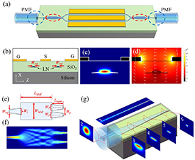
Figure 1. (a) Schematic of the presented EO modulator. (b) The cross-sectional geometry of the waveguides and the Cr–Au electrodes. (c) The simulated optical field of the TE mode. (d) The simulated electrostatic field of the arms. (e) and (f) The schematic and the simulation of the designed MMI coupler. (g) Schematic of the edge coupler. Inset 1: Finite difference time domain (FDTD) simulation of the field profile of the inverse taper. Inset 2: simulated mode field of the 5 μm PMF. Insets 3–6: simulated mode field distribution at different parts of the inverse taper.
Download figure:
Standard image High-resolution imageFigures 1(c) and (d) shows the simulated TE mode optical field and the electric field when applying a 1 V on the electrodes of the modulator arms. Two 1 × 2 MMIs are served as 3 dB beam splitters, marked with red dotted circles in figure 1(a). Figure 1(e) shows the design sketch of the MMI coupler, in which the input and output waveguides are adiabatically tapered with a length of Ltaper = 60 μm from a width of Wwg = 1 μm to Wt = 6 μm to achieve high waveguide to MMI coupling efficiency. The width and length of the MMI are designed to be WMMI = 20 μm and LMMI = 223 μm, respectively. The distance between the two waveguide arms is designed to be 10 μm for balancing the requirements on the footprint and cross talk. Figure 1(f) shows the FDTD simulation of the optimized MMI which resulting in a loss of 0.02 dB. As shown in figure 1(g), inverse taper coupler with decreasing thickness and increasing width is designed to reduce the mode mismatching between the PMF (i.e. with a mode field diameter of 5 μm) and the LN waveguide. The width and thickness of the end of the inverse is designed to be 5 μm and 50 nm to match the mode profile of the PMF. The taper was produced by covering the fabricated LN waveguide with a tape but leaving the taper area (i.e. the tail of the waveguide) open for the additional chemo-mechanical polish (CMP) process. In this case, the CMP will naturally result in an inverse taper with decreasing thickness. The simulated mode fields of the PMF and cross section at different part of the inverse taper can also be found in the insets of figure 1(g), while the inverse taper couplers are marked in blue dotted circles in figure 1(a). According to figure 1(g), the mode field size gradually increases along the inverse taper until a good match of the mode fields between the PMF and the LN waveguide can be achieved. A coupling efficiency of 1.2 dB/facet can be facilitated by the use of inverse taper as indicated in our simulation.
3. Details in device fabrication
The EO modulator is fabricated on a commercial x-cut LNOI wafer (NANOLN, Jinan Jingzheng Electronics Co., Ltd), the LN thin film with a thickness of 300 nm is bonded to a buried silica (SiO2) layer on a 500 μm thick silicon (Si) substrate. Specifically, the thickness of the SiO2 layer was chosen to be 4.7 μm to reduce the energy leakage into the Si substrate considering the expansion of the mode field near the end of the inverse taper edge coupler. The fabrication process is illustrated in figure 2. First, a 400 nm thick chromium (Cr) is deposited on the LNOI by magnetron sputtering, and then the LN waveguides are patterned by femtosecond laser direct writing and formed by CMP. The total time of femtosecond laser patterning of one 4 cm length EO modulator is approximately 5 min. More details on the PLACE fabrication process can be found in [21, 25]. By carefully controlling the parameters in the CMP, inverse tapers with gradually decreasing thickness can be formed on both sides of the EO modulator. Secondly, a cladding SiO2 layer with a thickness of 1.5 μm is deposited by PECVD, then a 10 nm thick Cr layer and a 500 nm thick Au layer is deposited successively by magnetron sputtering. Afterwards the micro-electrodes are fabricated by femtosecond laser ablation of the Cr–Au layer in a space selective manner. Finally, the inverse taper edge coupler undergoes a careful polish for smoothing the end facets and achieving a better mode field matching between the PMF and the edge coupler.

Figure 2. Illustration of the fabrication process. (a) Coating of a chromium on top of the LNOI. (b) Patterning the Cr and LN thin film using femtosecond laser space selective ablation. (c) Transferring the pattern to LN layer using CMP. (d) Removal of the residual Cr and conduction of another CMP. (e) Coating of a SiO2 layer using plasma enhanced chemical vapor deposition (PECVD). (f) Coating of the Cr–Au layer on the SiO2 cladding and formation of the electrodes by femtosecond laser ablation.
Download figure:
Standard image High-resolution image4. Results
4.1. Characterization of MMIs and inverse tapers
In the past, the propagation loss of the single mode LNOI waveguides fabricated using the same condition was measured to be 0.13 dB cm−1, and more details about the measurement can be found in [25]. To determine the loss of the MMI coupler, a cascaded MMI coupler tree as shown in its optical micrograph in figure 3(a) was fabricated together with the waveguides. The loss of individual MMI can be determined by comparing the losses incurred with increasing number of MMIs in the tree. Figure 3(b) shows the measured TE mode transmission at the wavelength of 1550 nm versus the number of MMIs normalized by the total loss in the MMI tree. The loss of the MMI is measured as ∼0.11 dB by the fitting line, which is higher than our simulation result (0.02 dB). This should be caused by the fabrication error of the MMI coupler.

Figure 3. (a) Optical micrograph of the cascaded MMI couplers configuration. (b) Measured TE mode transmission of the cascaded MMI couplers at the wavelength of 1550 nm. (c) Infrared CCD captured mode profile image at the wavelength of 1550 nm of the PMF fiber. (d) Infrared CCD captured mode profile image at the end of the edge coupler.
Download figure:
Standard image High-resolution imageWe measured the mode fields of the PMF and the edge coupler as shown in figures 3(c) and (d) respectively. The transverse size of the mode field of the PMF is close to that of the inversed taper, while the vertical size is larger than that of the inverse taper. To characterize the coupling loss, we fabricated a short straight waveguide (i.e. 5 mm length) with the inverse taper couplers at both ends. Considering the short propagation distance and the low propagation loss, it is reasonable to attribute the total loss to the coupling loss at the facets. As a result, the measured coupling loss of the fabricated inverse tapers at 1550 nm wavelength is 3.25 dB/facet, which is also higher than simulation result (1.2 dB/facet). This may also be due to the imperfection of the end facets and the fabrication error of the inverse tapers.
4.2. Characterization of LNOI-based EO modulator
To demonstrate the EO modulation performance of the fabricated device, we measured the Vπ of the modulator. Figure 4(a) shows the optical micrograph of the fabricated EO modulator. Figure 4(b) shows the zoom-in SEM image of the area indicated by the red dashed box in figure 4(a). The SEM images of the Cr–Au electrodes and the cross section of the single mode waveguide are shown in figures 4(c) and (d), respectively. The measured fiber-to-fiber insertion loss of the 4 cm length EO modulator is 7.6 dB. The static response of the modulator is measured by applying a triangle electric signal onto the modulator. As shown in figures 4(e) and (f), the Vπ is determined to be 0.84 V, with an extinction ratio of 25 dB. The HWV-length product (Vπ × L) is 3.4 V cm in this case. The relatively high Vπ × L is simply a result of the fact that the micro-electrodes are well separated from the LN waveguides by the 1.5 μm thickness SiO2 cladding layer.
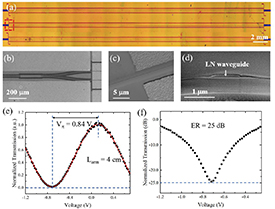
Figure 4. (a) Optical micrograph of the fabricated EO modulator. (b) The zoom-in SEM image of the area marked by the red dashed box in (a). (c) The SEM image of the fabricated Cr–Au electrodes. (d) The SEM image of the cross section of the single mode LN waveguide. (e), (f) The static EO performance of the fabricated modulator.
Download figure:
Standard image High-resolution imageWe also fabricated a 2 cm long EO modulator without the SiO2 cladding layer on the LN waveguides, therefore the electrodes can be fabricated in the same plane of the waveguides. In this case, we characterized the frequency response of the modulator device using the experimental setup illustrated in figure 5(a). An inline fiber polarization controller is used to ensure the TE mode from the laser at the input end. The output light from the modulator first passes through an erbium-doped fiber amplifier (EDFA) and then a band-pass filter (BPF) for achieving high signal to noise ratio before entering the photodiode (PD, New Focus 1014). A 6.5 GHz vector network analyzer (VNA, RIGOL RSA5065N) and a 10 GHz microwave probes (GGB model 10 A) are used for measuring the EO bandwidth (S21 parameter) of the fabricated device. The measured Vπ of the 2 cm EO modulator is 1.39 V, as shown in figure 5(b), corresponding to a Vπ × L of 2.8 V cm. The measured S21 parameter with an applied microwave frequency from direct current to 6.5 GHz is shown in figure 5(c), which has been calibrated by subtracting the radio frequency (RF) cable loss. The measurement result implies that the EO bandwidth of the fabricated modulator is greater than 6.5 GHz which is limited by the VNA bandwidth. The measured bandwidth also forces into the bandwidth evaluated as ∼34 GHz by the simulated velocity mismatch between the calculated phase index of 1.87 for the microwave and the group index of 1.98 for the optical wave considering the 2 cm length of the EO modulator. The evaluated RF loss is about 1 dB cm−1, considering the relatively narrow gap between the signal and ground of the electrodes. It should be noted that we have not carried out any optimization of the velocity matching between the optical wave and the applied microwave signal, nor the structure of the electrodes. The EO performance of the modulator device can be further improved by adopting a reasonable phase matching configuration.

Figure 5. (a) Schematic of the experimental setup for measuring the S21 parameter of the fabricated EO modulator chip. BPF, band-pass filter; EDFA, erbium doped fiber amplifier; DUT, device under test; FPC, fiber polarization controller; PD, photodiode; VNA, vector network analyzer. (b) and (c) Measured static EO performance and the S21 parameter of the fabricated 2 cm modulator.
Download figure:
Standard image High-resolution image
5. Discussion and conclusion
We have presented the primary results on an LNOI EO modulator fabricated using the PLACE technique. The technique features low propagation loss, high fabrication throughput, and large footprint. We have designed and fabricated low loss MMI as well as inverse taper using the PLACE technique, together of which has enabled low-loss EO modulators with a low Vπ of 0.84 V simply by increasing the arm length of MZI.
We consider that with the systematic investigations, the performance of MMI has approached that of theoretical prediction. The waveguide loss has almost reached the limited of absorption limited of LNOI. Therefore, to further promote the device performance, it is crucial to achieve better control on the mode profile conversion with the waveguide taper, which will be the focus of our next work.
On the EO modulation side, it is necessary to systematically optimize the phase matching between the microwave and optical field in the LNOI waveguides. The LNOI waveguide fabricated by PLACE technique is very different from the waveguide fabricated by EBL and ion dry etching in terms of the geometry and mode profile. For instance, the group index of the LNOI waveguide fabricated by PLACE is ∼1.98, which is significantly smaller than that of LNOI waveguide fabricated by EBL. However, the phase index of microwave can be easily tuned around 2 by choosing the proper combination of the materials and layer thicknesses of the cladding to achieve the satisfying phase matching between the microwave and optical wave. Last but not the least, it should be kept in mind that although an unconventional femtosecond laser writing process is involved in the PLACE fabrication technique, the other fabrication procedures including the CMP, cladding coating, microelectrodes fabrication, etc are all mature fabrication techniques employed by the photonics industry for many years. Thus we are optimistic about the reliability and sustainability of using the PLACE fabrication approaches in the future photonic integrated circuit industry.
Data availability statement
The data that support the findings of this study are available upon reasonable request from the authors.
Funding
National Key R&D Program of China (Grant No. 2019YFA0705000), National Natural Science Foundation of China (Grant Nos. 12004116, 11874154, 11734009, 11933005, 11874060, and 61991444), Shanghai Municipal Science and Technology Major Project (Grant No. 2019SHZDZX01).
Conflict of interest
The authors declare that there are no conflicts of interest related to this article.