

Abstract
A versatile van der Waals epitaxy of BiTe, a newly discovered dual TI and a predicted higher order topological insulator (HOTI) thin film on muscovite mica is demonstrated using pulsed laser deposition. Topographic, structural and XPS analyses confirm the chemical homogeneity and high crystalline quality with large-area coverage with atomically smooth surface. The magneto transport data reveals weak anti-localization and electron-electron interaction driven insulating ground state with n-type character. An elaborate thickness, temperature and magnetic field dependence of transport data indicates a transition from coupled, partially coupled and fully decoupled surface states wherein 3D electron-electron and electron-phonon scatterings play significant role in dephasing mechanism, unlike 2D electron-electron dephasing in most TIs. Also from the fitting of the resistivity upturn we found that the coulomb screening factor (F) in thicker samples turns out to be negative which indicates the presence of the electron phonon coupling in those samples.
Export citation and abstract BibTeX RIS
1. Introduction
Topological Insulators (TI) are the potential candidates for low power spintronics and quantum computing devices due to the spin-momentum locking of topological surface states (TSS) inhibiting direct backscattering [1–4]. The inherent layered structure of most TI favours van der Waals heteroepitaxy for exploiting the TSS properties in electronic devices. (Quasi) van der Waals (vdW) epitaxy of TI materials often involves the growth of TI on a 2D substrate or surface dangling bonds passivated substrates [5–7] resulting in only weakly bonded overlayer-underlayer vdW interaction with a sharp interface. Topological insulators are new class of quantum matter which exhibits a bulk insulating gap and gapless spin-momentum locked metallic surface states. In addition they emerged as a new platform for future spintronics applications owing to their fascinating properties such as suppression of back scattering, detection of Majorana fermion at the TI-superconductor interface [4] and so on. TI can be classified in two categories: strong TI having surface states (SS) at all the surfaces and weak TI having SS only at some specific orientations. Former has TSS at all its surfaces while the latter has TSS only at its side surfaces (not at the top and bottom and are being called the dark surfaces). Out of four Z2 invariants  which theoretically characterize a TI, a nontrivial ν0 index characterize a STI, whereas a WTI has ν0 having zero value and nonzero (ν1ν2ν3) indices, and consequently STI and WTI has odd and even number of Dirac surface states respectively [8]. WTI is comparatively new and has not been explored experimentally as much as STI [9–12].Theoretically it has been predicted that WTI has interlink with other new exotic topological phases such as Dirac Semimetal, Weyl Semimetal [12]. WTI can be exfoliated into 2D Quantum Spin Hall Insulator (QSHI) since WTI can be thought of being composed of 2D QSHI stacks [13].
Ever since the discovery of topological insulators,  has been studied extensively while the other members of the Bi-Te phase diagram like BiTe (Tsumoite),
  (Pilsenite) and so on are rather less studied. All the members of Bi-Te phase diagram can be represented using Bi2 bilayer (BL) and
  quintuple layer (QL) building blocks forming the homologous series
  where m and n are integers [14–20]. Since
  is a well-known 3D TI and Bi BL is predicted to be a 2D TI [21] , their combination is expected to exhibit topologically nontrivial properties [22, 23]. BiTe is the material which has a superlattice structure where one Bi BL is sandwiched between two
  QLs and recently BiTe has been reported as a Dual TI that is both WTI and Topological Crystalline Insulator (TCI) at the same time [22]. TCI is the topological phase of matter where the surface states are protected by mirror symmetry instead of time reversal symmetry [24]. Therefore, for a dual TI side surface states are protected by time reversal symmetry being a weak TI and the same on the dark surfaces by mirror symmetry being a TCI [22]. Thus, many new avenues can be explored by breaking these symmetries individually by applying strong magnetic field or structural modifications [22]. Very recently BiTe has been predicted to be a Higher Order Topological Insulator (HOTI) which means the material will be having hinge states or the corner states depending on the order and the dimensionality instead of having surface states [25, 26]. The growth of BiTe thin films on different substrates using PLD [27, 28], sputtering [29, 30], MBE [31–34], Hot-Wall epitaxy [35–37], and MOVPE [38] have been reported. However, detailed investigations on magneto transport characteristics from a topological insulator point of view and the dephasing mechanism are still lacking.
Here we report the magneto transport properties of epitaxial BiTe thin films grown on muscovite mica along with XRD, Raman, XPS, and AFM studies. 2D mica was chosen as the substrate owing to its chemically inert, highly insulating nature and most importantly, atomically smooth surface presenting pseudo-hexagonal lattice favorable for the van der Waals epitaxy [37, 39–45]. Additionally, it also serves an ideal template to obtain large area free-standing films which can be transferred to other substrates [44].Due to the bottom surface of the film and the top layer of the mica substrate, the disorder in the almost free standing film gets reduced down drastically since there is no dangling bond from the substrate affecting the film. The striking feature in transport data reveals that the dephasing mechanism in our film is 3D in nature and with the thickness large energy transfer process such as electron-phonon coupling emerges which is rarely seen in the topological insulator literatures. Now the electron phonon coupling has been studied in TI systems theoretically and investigated experimentally using ARPES [46–48]. Here, we are showing from the transport study that e-ph coupling is playing a dominant role in dephasing of electronic wave function in our samples at low temperatures. To have a comparison of the quality and the electronic transport properties of the BiTe film on mica we deposited the same film in the same condition on Si(111) also and the comparison led us to the conclusion that vdW epitaxy indeed enhanced the film quality and sets our assumption that the large energy transfer as the dephasing mechanism is consistently happening in the BiTe thin film on a firm base. This work paves the way for more advanced research on the exotic electronic transport properties of a dual TI, vdW epitaxy of TI and on the dissipation less flexible electronics [49] based on topological insulator.
2. Experimental
 thin films of five different thicknesses (10 nm, 30 nm, 45 nm, 74 nm, 125 nm) were deposited on muscovite mica substrate using pulsed laser deposition technique. The wavelength of the excimer laser was 248 nm and the pulse width was 20 ns. The energy of the laser beam on the target was fixed at 50 mJ and the frequency of the pulse was 3 Hz. The target was made by mixing ultra pure Bi powder (99.999%) and Te powder (99.999%) at a ratio of 1:1 and was annealed at 150 °C in rough vacuum (∼10−2mbar) to harden the target. Freshly cleaved mica substrate was introduced into the chamber and was evacuated to ≤3 × 10⁻⁵ mbar. BiTe film growth was optimized at 275 °C substrate temperature. Higher laser energy was found to preferentially deplete Te from the target due to its higher vapor pressure [50, 51]. Thus, a nearly congruent transfer of the target composition to the thin films was achieved with a better predeposition vacuum and lower laser fluence. As post-annealing turned out to increase the film roughness, post-annealing was avoided. Hall bar devices were readily achieved with physical masking and hence the contamination due to photoresist coating while doing optical lithography otherwise is avoided.
X-Ray Diffraction was done in a Rigaku diffractometer using Cu source (λ = 0.154 nm for Kα radiation) and working voltage 40 kV to check the phase and the orientation of our films. The pole diagram was obtained with the same system (medium resolution) where the diffraction angle (2θ) is fixed and the diffracted beam intensity is collected by varying two geometrical parameters, such as the χ angle (tilt angle from sample surface normal direction) and the ϕ rotation angle around sample surface normal direction. The diffracted intensity data is mapped into a polar plot as the sample is rotated 360° around azimuthal (ϕ) axis and tilted from 0° to 60° around the tilt (χ) axis. Atomic force microscopy (AFM) was performed in tapping mode in a BRUKER instrument to conclude the thickness and the surface topography of the films. The surface scans performed at 10 μm × 10 μm area. X-Ray photoemission spectroscopy (XPS) data was collected from Kratos Axis Ultra DLD system equipped with a monochromatic Al source (Kα − 1 486.6 eV) and beam spot size being 300 μm × 700 μm. Raman spectra was taken to confirm different characteristic vibrational modes using a Horiba LabRAM system where 532 nm wavelength laser was used.
The magneto transport measurements were done in Quantum Design PPMS 14 T with the temperature range 2 K to 300 K. Hall bar devices were mounted on the sample PUCK with the help of GE-Varnish glue for being electrically insulating but good thermally conducting. The contacts were given with copper wire and silver paint.
3. Results and discussion
BiTe belongs to  P-3m1 space group with lattice parameters a = 4.423Å and c = 24.002Å. Room temperature XRD of BiTe (125 nm) /mica heterostructure shown in figure 1(a). displays (00l) family of diffraction peaks along with substrate diffractions peaks indicating the c-axis preferential growth of BiTe. Kα, Kβ peaks of the substrate are also marked. XRD profile shows that all the sample peaks belong to
  and no other peaks are observed. Pole figure was recorded to investigate the relative in-plane orientation of
  epilayer formed on muscovite mica (0 0 1) substrate. Figure 1(b). depicts pole figure scan of 39 nm thick
  thin film around (1 0 9) reflection indicated by the inner six well-defined spots (at χ = 34.84◦) with azimuthal (ϕ) angular separation of 60◦, confirming the hexagonal symmetry present in
  layer. The outer six sharp poles with varying intensities are confirmed as the combination of (−1 3 5), (−1 −3 5), (1 −3 5), (1 3 5), (2 0 4) and (−2 0 6) peaks of monoclinic Mica substrate by considering the ϕ-shift ∼ 30° with respect to BiTe (1 0 9) reflections. From these results, the possible epitaxial relationships between the film and the substrate are established to be
  [0 1-1 1] ∥Mica [0 1 0] and
  [1 1-2 0] ∥Mica [1 0 0]. Despite large lattice mismatch (15%), this kind of incommensurate and relaxed epitaxial hetero-interface is mainly attributed to van der Waals epitaxy mechanism leading to nearly strain-free BiTe film grown on mica.
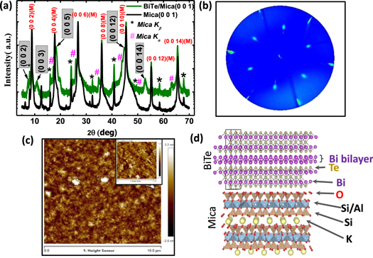
Figure 1. (a) XRD scan of  film on mica(001) and of bare mica, (b) Pole figure (log plot) of
  (1 0 9), (c) AFM image of the surface (10 μm × 10 μm area) topography of the BiTe film on Mica (Inset is 1 μm × 1 μm area scan), (d) Schematic illustration of
  /mica heterostructure via the van der Waals heteroepitaxy.
Download figure:
Standard image High-resolution imageAFM image figure 1(c) of a representative 125 nm film reveals smooth surface. There are no triangular or pyramidal or spiral growth features unlike most of the previous reports [31, 40, 41, 52, 53]. Rather the growth is continuous on mica and consequently the existence of terraces, valleys, gaps are absent [54]. The rms roughness of all the films (∼0.5nm) over scan area of 10 μm X 10 μm is comparable to the films grown by MBE implying the layer-by-layer high quality growth. This is attributed to the nature of van der Waals epitaxy (2D material on 2D substrate) which relieves the lattice matching conditions between the overlayer and substrate. That is why despite having lattice mismatch as high as 15 % the film topography is smooth. The 10 nm film is showing steps of around 0.1 nm which is absent in the other films (figure S1(a) available online at stacks.iop.org/MRX/6/126321/mmedia). This is probably because of the low thickness of the film. The inset of figure 1(c) shows a zoomed in scan of 1 μm2 area where the aforementioned statements can be verified. Figure 1(d) shows the schematic of van der Waals epitaxy of BiTe on mica. The hexagonal unit cell of BiTe is composed of a 12 atomic layers in the sequence (Te–Bi–Te–Bi–Te)-(Bi-Bi)-(Te–Bi–Te–Bi–Te)- with two mirrored hextuple layers of Te1–Bi1–Te2–Bi2–Te3–Bi3 on mica. Thus in a unit cell of BiTe, the middle Bi–Bi layer has weak covalent bond in between, whereas between 2 consecutive BiTe unit cell, that is between Te–Te layer there exist very weak vdW force. It is suggested that bonding between  QL and Bi BL stack is stronger than
  QL stacks.
Figure 2(a) shows the thickness dependent Raman spectra of BiTe/mica thin films along with bulk BiTe single crystal. The Raman peak positions at 59 cm−1 ( ), 90 cm−1(E1g), 101 cm−1(E2g), 118 cm−1 (A1g), 128 cm−1 correspond to degenerate in-plane vibrations of E symmetry and non-degenerate out-of-plane vibration of A symmetry. The Raman spectra is well described by the convolution of five Lorentzian line shapes as shown in figure 2(a). corresponding to different Raman active modes. The number of obtained peaks and their positions are consistent with earlier reports [15, 20, 27, 38], while no significant shift in peak positions of all the raman modes was observed with thickness ranging from ultrathin film to the bulk single crystal. This demonstrates that the BiTe epilayer has uniform strain and composition and supports the conjecture of a true vdW epitaxy. FWHM in figure 2(c). of 101cm−1(E2g), 118 cm−1 (A1g) tends to increase for lower thickness due to decrease in phonon lifetimes of interlayer modes [15] while the FWHM of 59cm−1 (
 ) and 90 cm−1(E1g) peaks do not show any significant trend. Figure 2(d). shows that the intensity ratios decrease as the thickness increases from the ultrathin films range to bulk. It is reasonable to assume that the out-of-plane vibrations compared to the in-plane vibrations will be less constrained in an ultrathin film than in bulk.

Figure 2. (a) Raman spectra of the films of different thicknesses and of a bulk single crystal, (b) Peak positions, (c) FWHM of different peaks, and (d) Different intensity ratios as a function of film thickness. The subscripts in the figure denotes the peak positions.
Download figure:
Standard image High-resolution imageXPS survey scan figure 3(a) on the 45 nm film indicates that all the major peaks are appearing from different Bi and Te orbitals. Carbon and oxygen peaks are there as usual and are relatively small [55]. The chemical states of Bismuth and Tellurium were obtained from the high resolution scan of the Bi 4f and Te 3d multiplets as shown in figures 3(b) and (c), respectively. These peaks were fitted with the Lorentzian function fits and the peak positions are Bi 4f7/2(157.5eV, 159.0 eV), Bi 4f5/2 (163.0 eV, 164.4 eV) and Te 3d5/2 (572.2 eV, 576.0 eV), Te 3d3/2 (582.5 eV, 586.3 eV), and their relative intensities are consistent with the previous reports [5, 56]. The low energy peaks in Bi 4f multiplets corresponds to Bi BL and display same intensity as core level of  QL [57, 58], in agreement with two different chemical states of Bi in BiTe. Each of these spin-orbit split doublets show a peak split of ∼145meV. The high energy peaks of Te 3d multiplets correspond to oxidized Te. The surface chemical stoichiometry is determined from the ratio of their areas turns out to be approximately 1. Thus, XPS data along with diffraction and topology results confirm the superstructure nature of BiTe. Similar signatures were observed even in polycrystalline BiTe thin film grown on Si(100) by MBE [57].
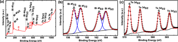
Figure 3. XPS (a) survey scan, (b), (c) High Resolution fixed scan of Bi 4f and Te 3d.
Download figure:
Standard image High-resolution imageResistance as a function of temperature from 2 K to 300 K of all the films in figure 4(a) depicts the metallic behavior which means that the Fermi level remains in the conduction band. The value of the Residual resistivity ratio,  =
= (∼1.4) characteristic of degenerate semiconductor or poor metal was observed. Even bulk polycrystalline BiTe system had exhibited a similar value compared to other members of the phase diagram which was assigned to the introduction of Bi BL in the unit cell [18]. For T < 10 K, the resistance of the films presents an upturn with logarithmic temperature dependence which can be attributed to disorder induced electron-electron interaction (EEI). The EEI correction to residual resistance in a quasi-2D limit is given by [59]

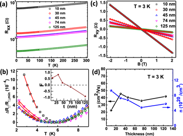
Figure 4. (a) Temperature dependent longitudinal resistance for different BiTe films, (b) Zoomed in image of the upturn in figures 4(a), (c) Hall resistance of different films at T = 3 K, (D) Hall mobility and carrier concentration as a function of thickness at T = 3 K.
Download figure:
Standard image High-resolution image
 is the sheet resistance, h is Planck's constant, F is the coulomb screening factor averaged over the Fermi surface and T0 is a reference temperature.(Here T0 is taken to be Tmin,the temperature corresponding to minimum resistance.) Tmin remains thicknees independent unlike ∼1/d dependence reported for bismuth telluro-sulfide [37]. Figure 4(b) displays the fits based on equation (1) and the extracted values of F for various thicknesses is shown in the inset. It is noteworthy that the coulomb screening factor F changes sign from positive to negative as the thickness increases. Samples from different batch with different thicknesses also matching with the trend (figures S1(b), (c)). However, the original theory by Altshular does not predict the negative value of F [59]. Negative values of F has been observed in TI materials wherein it was ascribed to the strong inherent spin–orbit coupling of the material [60]. However, Wu et al demonstrated empirically that F can take negative value if there is appreciable amount of electron-phonon coupling present in the sample [61]. They observed that with the introduction of spin–orbit coupling in TiAl alloys by diluting with heavy Au atoms, F became more negative. Thus, we believe that electron-phonon coupling with strong spin–orbit coupling gives rise to the negative F value. However, detailed theoretical study is needed to affirm whether such origin applies to TI systems or not [60]. On the other hand, the Weak Anti-localisation (WAL) correction to residual resistance is given by [62]

where α is number of coherent transport channels and β the dephasing index ( , details in the next section) obtained from magnetotransport data does not describe the data well (figure S1(d)). Hall effect measurements were performed on all the films at different temperatures from 2 K to 12 K up to 14 T to extract the carrier concentration and the mobility of our film. It has been observed that there is no non-linearity of the Hall data up to 14 T which reveals that there is only one type of carrier in our system and from the negative slope of the linear data we conclude that it is electron. Hall resistance as a function of magnetic field(up to ± 2 T) measured at 3 K for various thicknesses are plotted in figure 4(c). 14 T Hall data can be found in (figure S1(e)). Mobility (μ) comes out to be around 30 to 40 cm2/Vs for all the films and the carrier concentration (n) is ∼9 × 1020 cm−3 (figure 4(d)). For MBE grown
  and BiTe on lattice matched BaF2(111) substrate, the carrier concentration of BiTe was two orders of magnitude larger than
  implying that Bi-bilayers acts as electron donors [15] pushing the fermi level deep inside the conduction band while mobility falls off drastically by an order of magnitude ascribed to high degree of disorder corroborated by simulations of diffraction data. Disorder arises due to asynchronous incorporation of Bi bilayers across the surface during growth resulting in high density of domain boundaries in lateral direction [16]. The usual behavior of carrier concentration and mobility that increases and decreases respectively with temperature can be seen in our samples (figure S1(f)). It is noteworthy that the carrier concentration is reducing down with the increasing thickness (figure 4(d)), though no such trend follows for mobility.
Magnetoresistance measurements were performed up to 14 T with magnetic field applied perpendicular to the sample plane at various temperatures (figure S3(a)). The low-field magnetoresistance displays a sharp cusp (figure 5(a)) characterising weak anti-localization (WAL) effect which is a consequence of quantum destructive interference between two time reversed paths of electrons. As the field increases the MR becomes normal classical parabolic type as the electrons gain Aharonov–Bohm phase which eventually destroys the interference and in turn the WAL. The parabolic MR can be explained by the classical Drude model. The sharpness of characteristic WAL cusp also gets suppressed with increasing temperature (figure 5(b)). The low-field transverse magnetoresistance,  curves for various thicknesses at 2 K are shown in figure 5(a). It is to be noticed that the sharpness and magnitude of positive MR due to the WAL effect decreases with the film thickness. This is due the suppression of quantum interference effects in higher dimensionality that is when the thickness approaches from the thin limit to the bulk. The WAL effect can be analyzed using the reduced Hikami-Larkin-Nagaoka (HLN) formula for a system with very high spin–orbit coupling [63]:

where  is the sheet conductivity, α, the prefactor symbolizes the number of spin-orbit coupled coherent transport channels, lϕ, the phase coherence length signifies the length over which an electron can move without losing the phase of its eigenstate and ψ(x) is the diagamma function. In general, for 2D surface states in 3D TI, α ∼ 0.5 correponds to single spin-orbit coupled coherent surface channel while α ∼ 1 imply independent decoupled topological transport channels. Figure 5(b) depicts the low-field (upto 0.3 T) magnetoconductance data,
  (B), along with HLN fits (solid lines) for a representative BiTe thin film (30 nm) at various temperatures. The HLN fittings upto 0.3T for other films is shown in the (figure S2). The fitting for higher magnetic field upto 2T can be described by including additional B2 term to HLN equation (figures S3(b)–(f)) [64]. As it can be noticed that the quantum effect gets destroyed due to the randomisation of phase at higher temperature. The temperature dependence of extracted lϕ and α from HLN fits for various thicknesses are shown in figures 5(c) and (d), respectively. It can be seen from figure 5(c) that
  and exhibits a weak temperature dependence.
  for thinner samples (t ≤ 30 nm) indicates single coherent channel for electrically coupled two topological surface states. For thicker films,
  signifies that the surface states are completely decoupled generating two spin orbit coupled coherent channels. The gradual change of α from 0.5 to 1 with thickness indicates a transition from coupled, partially decoupled to fully decoupled topological surface states [65, 66]. The phase coherence length, lϕ for all thin films in figure 5(d) decreases monotonically with temperature and follows a power law,
  . The exponent β is predicted to have values 0.33, 0.50 and 0.75 corresponding to dephasing mechanism due to electron- electron scattering in 1D, 2D and 3D, respectively, while β ≥ 1 corresponds to the onset of electron-phonon coupling in 3D when large energy transfer scattering takes place [67]. It is clearly seen from figure 5(d) that β ∼ 0.75 for t ≤ 45nm and β ∼ 1 for thicker films highlighting 3D electron-electron scattreing and electron-phonon scattering as the major dephasing mechanism in our samples. This observation is in stark contrast with Nyquist 2D electron-electron dephasing mechanism reported for most of the TI materials where β ∼ 0.5. It is noteworthy that the fitting in figure 4(b) yielding negative F value also supports the presence of electron phonon coupling in those two thicker samples (74 nm and 125 nm). The Ioffe Regel value which is
  where kF is the fermi momentum, and the mean free path,
  .
.  implies that the transport is in weak disorder limit [64]. As the phase coherence length is larger than thickness (lϕ > t) for all the films at low temperatures, the dephasing should happen in 2D limit. But we observe the 3D large energy trasfer mechanism taking part in dephasing. Now, large energy transfer assisted dephasing (Elctron-phonon coupling) has been observed in TI material rarely [65, 68]. They have shown that in the 'clean limit' the large energy transfer processes dominates. Thus here we can conclude that our samples are in the clean limit or in the low disordered regime which is in accordance with the Ioffe Regel criterion. Moreover, the samples on the mica substrate are grown with van der Waal epitaxy which again lessen the substrate contribution in degrading the film quality.Therefore, 3D electron-electron and electron-phonon scatterings contribute to dephasing mechanism in our samples wherein the former dominates for lower thickness regime and the latter takes over as the deviation from the 2D limit to 3D limit is approached. It is to be noted that all these observations indicates that the large scale energy transfer prevails in the BiTe films unlike small energy transfer in most of the previous reports. Whether the unusual larger value of dephasing index β is a characteristic signature of a dual TI and a predicted to be HOTI like BiTe or not, needs to be investigated further on similar systems, if any.
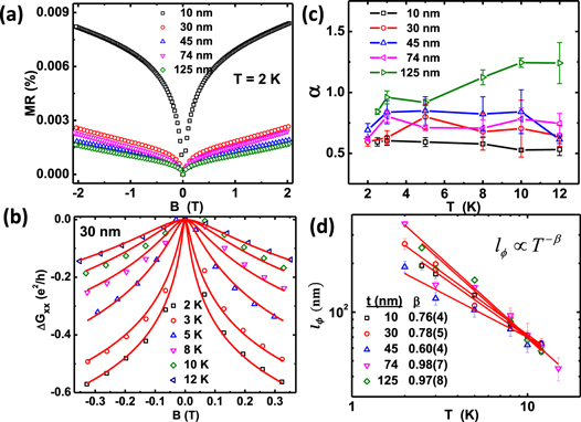
Figure 5. (a) Normalized magnetoresistance curve for different thicknesses at T = 2 K, (b)Low-field magnetoconductance data (symbols) along with HLN fit (solid red lines) for 30 nm BiTe thin film at various temperatures. Temperature dependence of extracted (c) α, the prefactor and (d) the phase coherence length (lϕ) versus Temperatrure for different thickness. Lower inset shows β for different thickness. Solid straight lines indicate the fitting.
Download figure:
Standard image High-resolution imageComparison with BiTe thin film deposited on Si(111):
High quality BiTe thin film (85 nm) was deposited on silicon (111) substrate keeping all the growth parameters constant while growing on mica to have a direct comparison of the quality and the transport properties. XRD confirms the phase and the (00l) orientation of the BiTe film on the Si(111) though unlike BiTe on mica, the appearance of an intense and non-oriented peak (104) indicates the polycrystalline nature (figure 6(a)). This is also corroborated by the phi scan performed around (109) peak of BiTe on Si(111) where a very broad peak with noisy background is seen. AFM image shows the granule nature of the film in sharp contrast to the AFM topography of the film on mica being continuous and showing no granularity and thereby increasing the rms roughness around 10 nm which is almost two orders higher than that on mica (figures 6(b), (c)). It should be noted that BiTe/Si(111) actually involves quasi-van der Waals epitaxy (2D/3D) where in the dangling bonds on the surface of the Si(111) are involved making the topography rough whereas BiTe/mica is purely van der Waals epitaxy (2D/2D) which does not involve any dangling bonds but rather weak van der Waals interaction between the over layer-substrate. Raman peak positions match with those from the films grown on mica and the BiTe single crystal (figure 6(d), single crystal raman data is in figure 2(a)). In this figure we have reused the XRD, AFM and the raman data of BiTe/mica to have a direct comparison.
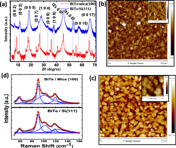
Figure 6. (a) Stack of XRD images of BiTe / Si (111) and BiTe / Mica(001) (only BiTe peaks are indexed here, no mica peak is indexed), (b), (c) AFM image (10 μm × 10 μm area) of the topography of BiTe/Si(111) and BiTe/Mica (001) respectively, (d) Stack of Raman shifts of BiTe/Mica (001) and BiTe/Si(111). (For comparison BiTe/Mica images have been reproduced).
Download figure:
Standard image High-resolution image
Figure 7. (a) Hall Data for BiTe (85nm)/Si(111), (b) longitudinal resistance versus Temperature, (c) Magnetoconductance data at different temperature, (d) α, the prefactor and (e) the phase coherence length (lϕ) versus temperature. Straight lines indicate the fitting.
Download figure:
Standard image High-resolution image
Resistance versus temperature curve shows metallic nature and the upturn shows up at around 12 K (figure 7(b)). The main difference is that around 150 K the resistance turns down which is because at higher temperature the silicon substrate, being a good semiconductor starts contributing to the film conductance whereas this downturn is absent in the insulating mica substrate. Linear Hall data yields the electron concentration to be 2 × 1020 cm−3 and mobility (10 cm2 Vs−1) is less than those on the films on mica due to lot of grain boundaries owing to the granule nature of the film (figure 7(a)). The carrier mobility of BiTe on mica is higher by a factor of 3 compared to that on Si(111) substrate, which can be attributed to the superior quality and the reduced defect density in the BiTe films grown by van der Waals epitaxy. The disorder defining Ioffe-Regel parameter  which is almost one order less than the films on mica also implies that the BiTe / Si(111) is more disordered than the films grown on mica. In the same manner as BiTe/Mica the WAL has been analysed with the HLN equation (figure 7(c)). α takes value from 0.9 to 1.4 with the increasing temperature indicating that the surface states are completely decoupled irrespective of temperature (figure 7(d)). lϕ versus T exponent (0.78) supports the large energy transfer process (3D electron-electron coupling) even also in the film grown on Si(111) (figure 7(d)) as the dephasing mechanism which is in good agreement with films on mica. This confirms robustness of the dephasing mechanism in dual TI BiTe involving the large energy transfer processes (3D electron-electron scattering, electron-phonon scattering) irrespective of the substrate used. The following table shows the comparison of the various parameters for the film on both the substrates.
| Substrate | t | Rq | μ | n |

|
α | Lϕ | β |
|---|---|---|---|---|---|---|---|---|
| (nm) | (nm) | (cm2 Vs−1) | (1020 cm−3) | (nm) | (Lϕ ∼  ) ) |
|||
| Mica(001) | 74 | 0.5 | 35 | 5 | 14 | 0.8 | 350 | 0.98 |
| Si(111) | 85 | 10 | 10 | 2 | 2 | 0.9 | 275 | 0.78 |
4. Conclusion
In summary, atomically smooth thin films of the newly discovered dual topolological insualator BiTe, predicted to be a higher order topological insualtor (HOTI) due to its non vanishing mirror chern number, has been grown on muscovite mica via van der Waals heteroepitaxy. The phase purity and the epitaxial relation between mica and BiTe thin film were established by the XRD and the pole figure. RMS roughness from AFM measurements were found to be around 0.5 nm which proves the films are atomically smooth. XPS study proves that the Bismuth is present in the sample in two different environments, one in Bismuth bilayer and the another one in the  quintuple layer as BiTe consists of one Bi bilayer sandwiched between two
  quintuple layer. The low energy peaks of the Bi 4f multiplets are from the Bi bilayer and the higher energy peaks are from the Bi in the quintuple layer. The electron concentration estimated from linear Hall data comes out to be ∼9 × 1020 cm−3. This large carrier concentration and the metallic resistance versus temperature curve indicate that the Fermi level is deep inside the conduction band. The low temperature resistivity upturn is well described by the electron-electron interaction correction to the residual resistance in quasi-2D limit. From this fitting we extracted the value of the Coulomb scattering factor F. The unusual transition of F from positive to negative value with increasing thickness signifies the emergence of electron-phonon coupling in thicker samples. The low-field magnetoresistance displays a sharp cusp characterising weak anti-localization (WAL) effect which is the consequence of quantum destructive interference between two time reversed paths of electrons. The fitting of these low field magnetoresistance data at various temperatures is done using HLN equation. The prefactor α in HLN equation transits from 0.5 to 1 in thicker samples which denotes the decoupling of the surface states at the higher thickesses. Another fitting parameter in HLN equation, the phase coherence length, lϕ for all thin films decreases monotonically with temperature and follows a power law,
  . The dephasing index β takes value ∼1 which again highlights the presence of electron-phonon coupling in thicker films. Now it is intriguing why high energy transfer processes (e-ph coupling or 3D e-e coupling) is showing up consistently in this predicted HOTI material and naturally it attracts more advanced research.
When the same system is grown on a different substrate Si(111) then both the disorder and the AFM roughness change. There is no epitaxial relation observed in this case. The AFM roughness almost increases 20 times and the Ioffe-Regel value  falls down from 14 to 2 when grown on Si. Naturally lϕ also decreases from 375 nm to 275 nm. These all yield a clear picture of van der Waals epitaxy that is 2D material grown on 2D substrate. Since mica is a good exfoliable 2D material there is no dangling bond and this improves the film quality minimising the disorder and make it atomically smooth. Magnetotransport data shows that the surface states are decoupled and from
  curve it is evident that the large energy transfer assisted dephasing process(3D electron-electron coupling) still prevails in the film on Si.
Our magnetotransport study basically probes the parallel combination of the surface states and the bulk of BiTe, a predicted HOTI. Thus our experiments immediately call for the magnetotransport study of the side surfaces where the contact probes can probe the edge states and show the quantized Hall effect in 3D shedding light on Higher Order Topological Insulator [69]. In addition, large area, high crystalline TI on flexible mica will open up more extensive and advanced research for future flexible and dissipation less spintronics applications.
Acknowledgments
We thank Bhawana Mali, Anomitra Sil, Amrit Raj, Shwetha Bhat and Arun M Chowdhury for discussion and their help. DM and SM thank MHRD, Govt. of India. Y Bitla acknowledges the financial support from the UGC under Dr. D S Kothari postdoctoral fellowship scheme F.4-2/2006 (BSR)/PH/16-17/0077. PSAK acknowledges Nanomission, DST, India for financial support.