

Abstract
ZnO nanostructured films were prepared by a chemical bath deposition method on glass substrates without any assistance of either microwave or high pressure autoclaves. The effect of solute concentration on the pure wurtzite ZnO nanostructure morphologies is studied. The control of the solute concentration helps to control the nanostructure to form nano-needles, and -rods. X-ray diffraction (XRD) studies revealed highly c-axis oriented thin films. Scanning electron microscopy (SEM) confirms the modification of the nanostructure dependent on the concentration. Transmission electron microscopy (TEM) results show the single crystalline electron diffraction pattern, indicating high quality nano-material. UV–vis results show the variation in the band gap from 3.20 eV to 3.14 eV with increasing concentration as the nanostructures change from needle- to rod-like. Photoluminescence (PL) data indicate the existence of defects in the nanomaterials emitting light in the yellow–green region, with broad UV and visible spectra. A sharp and strong peak is observed at ∼438 cm−1 by Raman spectroscopy, assigned to the  optical mode of ZnO, the characteristic peak for the highly-crystalline wurtzite hexagonal phase. The solute concentration significantly affects the formation of defect states in the nanostructured films, and as a result, it alters the structural and optical properties. Current–voltage characteristics alter with the measurement environment, indicating potential sensor applications.
Export citation and abstract BibTeX RIS
1. Introduction
Over the past few decades, extensive studies on zinc oxide (ZnO) have been carried out for its applications in different electro-optical industries and technologies, such as spintronics devices [1], light emitting [2] and laser diodes [3] surface acoustic wave devices [4], and transparent electrodes for photovoltaic (solar) cells [5] and field emission displays [6]. For the progress of ZnO-based optoelectronic devices, it is indispensable to grow high-quality ZnO thin films with both n-type and p-type electrical conductivity. As-grown ZnO is a II-VI transparent n-type metal oxide semiconductor with a wide direct band gap (3.37 eV) and a large exciton binding energy of 60 meV at room temperature [7, 8], which makes ZnO an attractive material for an extraordinarily widespread range of potential opto-electronic applications such as UV lasers [9], thin film transistors [10], UV detectors [7], piezoelectric devices [11], gas sensors [12], and also biomedical applications such as antibacterial and antifungal agents [13]. In addition to its UV excitonic emission peak, ZnO usually shows visible luminescence at varied emission wavelengths owing to intrinsic or extrinsic defects [14]. However, for these applications and generating well-ordered defects, it is crucial to control the shape, size and crystallinity of ZnO nanostructures, since the physical and chemical properties are meticulously dependent on them. In the past few years, researchers have successfully synthesized diverse types of ZnO nanostructures like nano-plates [15], nano-tubes [16], nano-flowers [17], nano-rods and nano-belts [18, 19]. Among these nanostructures, preferentially aligned vertical and dense nano-rods on a desired substrate can potentially deliver a striking solution to achieve excellent properties for applications such as energy harvesting devices, field emission displays, and light emitting diodes. The use of nanoscale devices and systems is desirable as scientific society is facing a wide range of challenges to accomplish the requisite. There are several methods to achieve controlled ZnO nanostructures, such as chemical bath deposition [15], chemical vapor deposition [20], electrodeposition [21], electrospinning [22], precipitation methods [23], laser assisted flow deposition [24] and hydrothermal techniques [25–28]. Among all of these different aforementioned methods, the chemical bath deposition method is simple and economical, with external conditions such as the pH value, reaction temperature, reaction time, and solution concentration are the only critical parameters that will affect the reaction rate and the morphology of ZnO. In the present investigation, we have utilized the chemical bath deposition method to grow highly oriented ZnO films and have studied the effect of solute concentration on the structural, optical and electrical properties. By controlling the solute concentration, the morphology has been controlled in the form of needles and rods, and characterization has been performed by different techniques as discussed in this report. In addition, we explore the possibility of using this material in sensing applications by measuring current–voltage characteristics in different environments like air, ethanol and acetone.
2. Experimental techniques
2.1. Synthesis process
Concentration dependent ZnO nanostructure films on glass substrates were synthesized by a simple and economical chemical bath deposition process in the desired scale with different morphologies like needles and rods. Aqueous solutions of (Zn(NO3)2.6H2O) salt (50–250 mM in intervals of 50 mM, Alfa Aesar Chemicals) made by adding the appropriate quantity of double distilled (DD) water were used as starting materials. After complete dissolution of the solute in DD water, ammonia was added dropwise and the mixture was maintained at pH ∼ 12. Glass substrates were used as they are cheap and suitable for many optical devices. Well cleaned glass substrates were kept vertically in the reaction solution. To understand the growth mechanism more clearly, the reaction temperature (120 °C) and time (∼90 min) were kept constant. After completion of the reaction time, the coated films were taken out of the solution and rinsed carefully in distilled water several times to remove excess ammonia from the substrate, followed by annealing in air at 300 °C for 2 h to get pure phase ZnO nanostructures.
2.2. Experimental details
The phase formation and surface morphology of the ZnO films were characterized by x-ray diffraction (XRD, Bruker D8 Advance x-ray diffractometer) with Cu-Kα radiation (λ = 1.54 Å) and field emission scanning electron microscopy (FESEM, Supra 55 Zeiss), respectively. Additional structure analysis of distinct nanostructures was carried out using transmission electron microscopy (TEM). TEM images were taken by HRTEM, JEOL JEM 2100 and JEOL 3010 instruments with a UHR pole piece with selective area electronic diffraction (SAED). Optical band gaps were determined using a diffuse reflectance spectrometer (Agilent Cary-60 UV–vis). Room temperature photoluminescence (PL) spectra of ZnO films were determined using a Dongwoo Optron spectrophotometer. The excitation wavelength was fixed at 325 nm and emission spectra were scanned from 350 to 850 nm. Micro Raman scattering of the samples was recorded using a Labram-HR 800 spectrometer equipped with excitation radiation at a 488 nm wavelength by an argon ion laser at a spectral resolution of about 1 cm−1. The I–V characteristics of ZnO in the presence of different atmospheres were measured by using a programmable Keithley source meter 2401.
3. Results and discussion
XRD measurements were accomplished to examine the crystal structure and phase purity of ZnO nano-needle and -rod arrays. Figure 1 shows the XRD patterns of the ZnO nanostructures on glass substrates with different concentrations, (a) 50 mM, (b) 100 mM, (c) 150 mM, (d) 200 mM, and (e) 250 mM deposited at constant temperature and time (120 °C and 90 min).
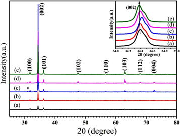
Figure 1. XRD patterns of ZnO nanostructures synthesized at different concentrations, (a) 50 mM, (b) 100 mM, (c) 150 mM, (d) 200 mM and (e) 250 mM (at deposition temperature 120 °C).
Download figure:
Standard image High-resolution imageAll the major peaks in the range 2θ ∼ 25°–80° of all of the films can be indexed to hexagonal phase wurtzite ZnO (space group P63mc), which are in agreement with JCPDS card number 80-0075, suggesting that the films are phase pure. However, a very low intensity peak near 2θ = 31.03° is observed for Zn(OH)2. It is evidenced from figure 1 that all films show strong directional growth along (002), which is unusual compared to other ZnO nanostructures [29, 30]. Figure 1 shows the negligible variation in peak position with the variation in concentration of the ZnO film; this indicates that the lattice parameters change insignificantly with changing concentration of ZnO.
Rietveld refinement (figure 2(a)) was performed using 'Fullprof' software and the values of the refined lattice parameters obtained from Rietveld fitting are shown in figure2(b). Figure2(b) shows the variation of lattice parameters as a function of concentration. The concentration shows a negligibly small effect on the lattice parameters. There might be probable reasons for the nonsystematic change in lattice parameter with concentration, due to internal compressive micro strain [31]. For size determination and to examine the effect of strain developed in the nanostructures grown on the glass substrates, the nanostructures were analyzed using the Debye Scherrer formula and a Williamson–Hall [32] plot using the uniform deformation model (UDM) (table 1). These are expressed as:

and

where D = crystalline size, K = shape factor (0.9), λ = wavelength of Cukα radiation and βD is the full width at half maximum of the corresponding peak, and  is the induced strain value.
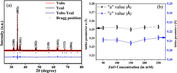
Figure 2. (a) Rietveld refinement of ZnO deposited with a concentration of 250 mM. (b) The lattice parameter variation in ZnO with different concentrations.
Download figure:
Standard image High-resolution imageTable 1.
The values of crystalline size and strain ( ) for the ZnO nanostructures grown at different concentrations obtained by Debye Scherrer's method and the Williamson–Hall method.
| Debye Scherrer's method | Williamson–Hall method Uniform Deformation Model (UDM) | ||
|---|---|---|---|
| Sample | D (nm) | D (nm) | Strain () × 10−3 |
| 50 mM | 45.715 | 46.321 | 1.92 |
| 100 mM | 46.205 | 46.986 | 2.40 |
| 150 mM | 47.259 | 48.171 | 2.69 |
| 200 mM | 48.361 | 49.356 | 2.80 |
| 250 mM | 49.500 | 50.608 | 2.97 |
All of the parameters obtained by using Debye Scherrer's and Williamson–Hall formulae are listed in table 1. From table 1 it can be seen that the strain is dependent on the crystallite size of the nanostructures and the higher the crystallite size, the higher is the strain and vice versa.
The variation of the surface morphology with solute concentration for the deposition of ZnO nanostructured films was studied by FESEM and is represented in figure 3. It shows that the film surface consists of nano-needles, tapered nano-rods and nano-rod-like microstructures with average length of 3 μm to 7 μm and average diameter of 100 nm to 600 nm. All films are composed of nano-needle- or nano-rod-like structures. With increase in the concentration, an increase in the diameter of the nano-needles/rods was found (∼150 nm, ∼200 nm, ∼450 nm, ∼600 nm and ∼650 nm for 50 mM, 100 mM, 150 mM, 200 mM and 250 mM, respectively). Higher concentration produces a micro-sized diameter with densely packed c-axis aligned ZnO rods, as shown in figure3(e). ZnO films deposited at lower concentration (50 mM) show tower (needle) shape nano-rods. As the solute concentration of ZnO increased, due to the high nucleation growth, nano-needles/rods start the stacking of flat tips, i.e. splitting of bigger rods into smaller rods, which is very common in ZnO [27]. With further increase in the concentration, the diameter of the nano-rods increases to give a flat tip-like nano-rod with larger diameter. The screw dislocation nucleation mechanism is one of the responsible mechanisms for nano-needles and rods, as reported in [28, 33], as we can rule out the layer by layer deposition mechanism [28]. Figure 4 shows a schematic of the transformation of nano-needes to nano-rods with variation in concentration during the synthesis of ZnO films. It is clear from this schematic and the FESEM images that lower concentration results in needles and higher concentration results in rods.
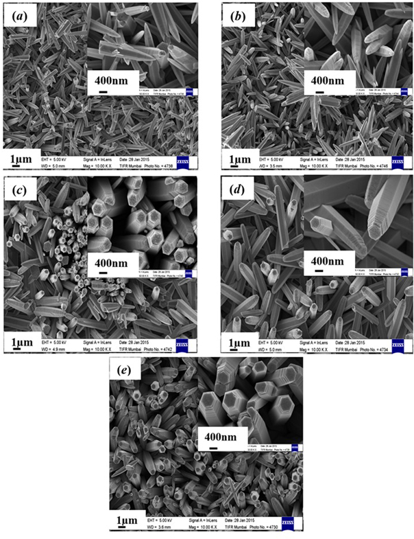
Figure 3. 10 KX FESEM images of ZnO deposited on glass substrates at different concentrations of (a) 50 mM, (b) 100 mM, (c) 150 mM, (d) 200 mM and (e) 250 mM. (Inset figure shows images at 50 KX.)
Download figure:
Standard image High-resolution image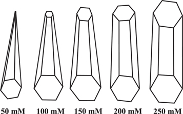
Figure 4. Schematic diagram representing the effect of solution concentration on the growth mechanism of the ZnO nanostructures.
Download figure:
Standard image High-resolution imageThe size and morphology of the ZnO nanostructures is analyzed by TEM and is represented in figure 5. Figure 5 (a) shows a TEM image of one of the ZnO nano-rods synthesized (100 mM) by the chemical bath deposition method. It shows a ZnO nano-rod with a diameter around ∼200 nm. Also, the corresponding SAED pattern (figure 5 (b)) confirms that the nano-rod has a single-crystalline wurtzite structure growing along the c-axis. XRD and TEM confirm that the present employed method results in nanomaterials with c-axis orientation, irrespective of the concentration, which is very useful for opto-electronic device fabrication.
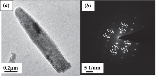
Figure 5. (a) Transmission electron microscopy (TEM) image of a single ZnO nano-rod (b) Selected area electronic diffraction (SAED) pattern of the nano-rod structure. The planes from which the electron beam was diffracted to generate the diffraction pattern are indexed in the diffractogram.
Download figure:
Standard image High-resolution imageRoom temperature UV–vis spectroscopy (in the range 300 to 800 nm) was used to obtain the intrinsic optical properties (band gap) of the ZnO nanostructures synthesized at different concentrations. Figure 6 shows the UV-visible spectra of ZnO in the range 380 nm to 425 nm. It is noticeable that the band gap varies from 3.20 eV to 3.14 eV as the concentration increases, which is due to the change in morphology of ZnO nanostructures from nano-needles to nano-rods. This result clearly indicates that the optical properties like the band gap of ZnO strongly depend on the morphology of the nanostructures. The band gap was determined using the Kubelka–Munk method [34].
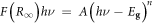
where F(R∞) is the Kubelka–Munk function, A is a constant, Eg is the band gap value and n is a unitless parameter with a value of 2 or ½ for indirect or direct band gap semiconductors, respectively [35].
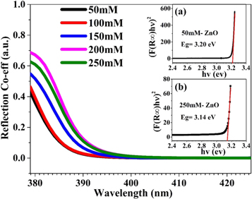
Figure 6. Room temperature UV–vis reflection spectra measured on ZnO nanostructure films deposited on glass substrates at different concentrations. (Inset figures (a) and (b) show extrapolation lines for 50 mM and 250 mM.)
Download figure:
Standard image High-resolution imageAs typical examples, the Tauc plots for the ZnO 50 mM and 250 mM samples are shown in the insets figures 6(a) and (b). From the insets, it is very clearly seen that the band gap is high (∼3.20 eV) at the 50 mM concentration and smaller (∼3.14 eV) at the higher concentration of 250 mM. Figure 7 shows the variation in band gap values calculated using the Kubelka–Munk method. It is clearly reflected that with increasing solute concentration of ZnO, the near band edge (NBE) peak position shifts to the lower energy side.
Figure 7. Effect of concentration on the band gap of ZnO nanostructures.
Download figure:
Standard image High-resolution imagePL spectroscopy is an effective method to investigate the presence of defects in semiconductors. The PL spectrum of the ZnO nanostructure depended on the preparation conditions (deposition time and temperature, concentration, etc). Figure 8 displays the room temperature PL of ZnO nanostructures synthesized at different concentrations with an excitation wavelength of 325 nm. It is evident from figure 8 that all films contain two main peak regions, one peak belongs to the UV region and another one fits to broad green–yellow emission in the visible luminescence (VL) region. This indicates that as we increase the concentration, the intensity of the VL region increases then decreases. This indicates that with increasing concentration, there is an increase in defect levels up to 200 mM and then a decrease.
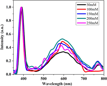
Figure 8. Room temperature normalized PL spectra of ZnO deposited at different concentrations.
Download figure:
Standard image High-resolution imageFigure 9 demonstrates the room temperature PL spectra and fitting curves of ZnO (200 mM) spread over a broad range from 350 to 800 nm (3.2 eV to 1.60 eV) measured by exciting with an energy of 325 nm. The typical wide emission spectrum of the ZnO nanostructures extending from NBE emission to red emission can be fitted by 12 well-resolved peaks. In ZnO nanostructures, the existence of defects is very well known, and defects including zinc vacancies (VZn), zinc interstitials (Znin), oxygen interstitials (Oin), oxygen vacancies (VO), and antisite oxygen have been reported previously. From the PL spectrum, a very strong band edge (ultraviolet at 387 nm) is observed resulting from the NBE emission of the wide band gap ZnO, while in addition to the UV excitonic emission peak, ZnO commonly exhibits visible luminescence at different emission wavelengths due to intrinsic or extrinsic defects [27]. We observed violet emission at 401 nm, which is believed to result from zinc vacancies (VZn) [36]. There is blue emission at 440 nm and 489 nm, which arises from the transition between the conduction band and zinc vacancies or zinc interstitials to zinc vacancies. However, the origin of these emission bands is not very clear.
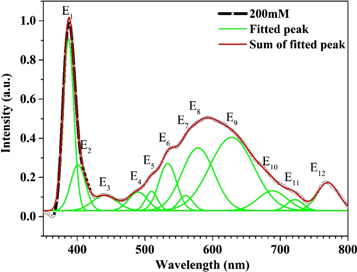
Figure 9. Room temperature PL spectra (black dots), Gaussian fitting curves (green) and summation of Gaussian curves (red line) of ZnO film grown at 200 mM concentration.
Download figure:
Standard image High-resolution imageWe also see another controversial issue is related to green emission, whose origin is unknown, at 509 nm, 533 nm, and 560 nm. These emission bands are either related to oxygen deficiency, i.e. from the conduction band to oxygen vacancies or zinc vacancies that are not distinguishable. The yellow emission at ∼578 nm is weak and wider, and is associated with an excess of oxygen [37] and arises from the transition from the conduction band to oxygen interstitials. Finally, small red emission bands around 628 nm, 688 nm, 721 nm and 769 nm are observed. The origin of the red emission is divided into two parts; first the red emission ranging from 620 nm to 690 nm can be attributed to oxygen interstitials, while that in the range 690 nm to 750 nm can be attributed to oxygen vacancies. In our case, the progressive change in yellow light emission intensity relative to UV emission suggests that there is a greater fraction of oxygen interstitials in these nano-rods. The intensity of this peak varies with the crystallinity of the ZnO nanostructures, as predicted. Hence, the PL of the ZnO microstructures can be prudently employed by changing their morphologies. All the peaks present and the possible defects causing the PL are summarized in table 2. These emission peaks in the visible region enable the thin films for application as laser diodes and light emitting diodes. The PL spectra are strongly dependent on the crystalline nature of the films.
Table 2. PL peak positions and respective defects assigned in ZnO nanostructures.
| Peak | Wavelength (nm) | Proposed deep level transition (color emission) |
|---|---|---|
| E1 | 387 | Near band edge emission [27] |
| E2 | 401 | Related to VZn(violet emission) [36] |
| E3, E4 | 440, 489 | CB to VZn or Znin to VZn (blue emission) [21, 37] |
| E5, E6, E7 | 509, 533, 560 | CB to VO or to VZn(green emission) [38, 39] |
| E8 | 578 | CB to Oi (yellow emission) [40–42] |
| E9, E10, E11, E12 | 628, 688, 721, 769 | due to lattice disorder along c-axis, (Zni defect) (red emission) [43] |
The wurtzite-type structure of ZnO indicates a basic unit of four atoms per unit cell with space group  Due to the four atoms in the unit cell, ZnO has a total of 12 phonon modes, with 3 acoustic modes (one LA, two TA) and 9 optical phonons (three LO, six TO). At the Γ-point of the Brillouin zone, the irreducible representation of the optical phonon is: Γ = A1 + 2B1 + E1 + 2E2 [44, 45], whereas the E modes are double fold degenerate, namely E2 (high) and E2 (low) related to the motion of oxygen and the Zn sub-lattice, respectively [44]. A1 and E1 are IR and Raman-active, E2 non-polar branches and only Raman-active while B1 modes are silent (inactive mode), i.e. both IR and Raman inactive. Figure 10 shows the room temperature Raman spectra of ZnO for optical properties investigation and the peak positions appearing in all samples in Raman are summarized in table 3. Figure 10 indicates seven peaks, sharp and intense peaks detected at 98.6 cm−1 (P1) and 438.5 cm−1(P6) are assigned to
  (low frequency) and
  (high frequency) and are related to the signal of Zn and the oxygen sub-lattice, respectively. A strong
  optical mode indicates a characteristic Raman active peak for the hexagonal wurtzite phase of ZnO and good crystallinity [46]. A small peak due to the multi-phonon process is detected at 332.4 cm−1(P3), and is assigned to
  -
- and recognized as a second order vibration mode arising from the zone boundary phonon. An additional low intensity peak is perceived at 382.8 cm−1 (P4) and allocated to the A1(TO) mode. In addition, there are two small peaks at around 411.1 cm−1 (P5) and 581.2 cm−1 (P7) assigned to E1(TO) and E1(LO), respectively [47, 48]. This E1(LO) mode is related to the existence of defects corresponding to interstitial Zn, oxygen vacancies, or their complex and indicates that the prepared ZnO nano-rods have good optical features. We also observed secondary mode vibration at 150 cm−1 and assigned it as a 2
 mode[49]. There are no obvious change in the Raman peaks except for a shift in E1(LO).
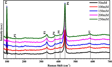
Figure 10. Room temperature Raman spectra of ZnO films ranging from wave number 80 cm−1 to 700 cm−1.
Download figure:
Standard image High-resolution imageTable 3. Summary of the phonon mode frequencies (in units of cm−1) of wurtzite ZnO films deposited at different concentrations.
| Positions of the vibrations bands (cm−1) | ||||||
|---|---|---|---|---|---|---|
| Peak no. | ZnO (50 mM) | ZnO (100 mM) | ZnO (150 mM) | ZnO (200 mM) | ZnO (250 mM) | Assignment |
| 1 | 98.64 | 99.17 | 99.37 | 99.37 | 99.37 | E2(low) |
| 2 | 150.38 | 151.62 | 150.38 | 151.62 | 151.62 | 2E2(low) |
| 3 | 332.49 | 333.59 | 332.59 | 333.44 | 333.59 | E2(high)-E2(low) |
| 4 | 382.81 | 380.42 | 380.97 | 380.97 | 382.21 | A1(TO) |
| 5 | 411.28 | 411.28 | 411.32 | 412.52 | 411.97 | E1(TO) |
| 6 | 438.57 | 438.28 | 438.57 | 438.42 | 438.71 | E2(high) |
| 7 | 581.26 | 581.26 | 580.02 | 584.84 | 587.32 | E1(LO) |
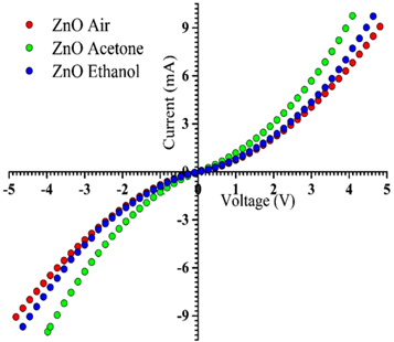
Figure 11 depicts the current–voltage (I–V) characteristics for ZnO in air, acetone and ethanol atmosphere. The I–V features appear to be symmetric with respect to the bias. Consistent and accurate results could only be obtained with a combination of Ohm's law for low voltages, as Ohm's law is generally valid for the low-voltage intrinsic regime of a low-conductivity material [50]. The entire I-V characteristics reveal good rectification behavior of the Schottky diodes. Figure 11 shows the room temperature I–V characteristics of ZnO nano-rods under different environmental conditions i.e. in the presence of air, acetone and ethanol. ZnO films show a nearly linear graph and follow Ohm's law for low voltage under all conditions.
Figure 11. Current–voltage characteristics of ZnO in air, ethanol and acetone atmosphere at room temperature.
Download figure:
Standard image High-resolution image
Metal oxide semiconductors are good gas sensors, which work on the principle of a change in electrical conductivity due to the chemisorption of the tested gas on the surface of the sensors [51]. In the case of n-type ZnO based sensors, they use a change in electrical conductivity for detecting gases. When the ZnO nano-rods are exposed to air, oxygen molecules absorb on the surface of the nano-rods because of oxygen deficiency in the zinc oxide nano-rods and form oxygen ions such as O2−, O2−or O− ions by capturing an electron from the conduction band, which results in an increase of resistance [52]. When the ZnO nano-rods are exposed to other atmospheres, i.e. ethanol or acetone atmosphere, these gases are adsorbed on the surface of the ZnO nano-rods, they capture the oxygen ions from the surface of the nano-rods and form a by-product which gives free electrons to the conduction band [52, 53]. As a result, there is an increase in free electrons in the conduction band which increases the electrical conductivity. Figure 11 shows a considerable change in current when the ZnO film is exposed to ethanol and acetone environments at room temperature. In the case of acetone, the current is greater as compared to ethanol because acetone is easily converted into vapor at room temperature and hence is easily detected by sensor. The current under reverse bias and forward bias is higher in the cases of acetone and ethanol atmospheres as compared to air, indicating the increase in carrier concentration by changing the atmosphere. From this, we conclude that ZnO nano-rods are a good sensor for detection of acetone and ethanol at room temperature.
4. Conclusion
A simple technique for the well-ordered growth of ZnO nano-needles and nano-rods on glass substrates by controlling merely the concentration of ZnO is established. XRD studies indicate that the films are preferentially c-axis oriented. Rietveld refinement confirms alteration of the lattice constant with increasing concentration. The SEM images clearly indicate the change in the ZnO morphology with different concentration with lower deposition temperature (120 °C) and time (90 min): needle flowers at 50 mM and 100 mM, and rod-flowers at (150 mM to 250 mM). Depending on the morphology, which affects the optical properties, naturally the band gap was found to vary. The lower the concentration, the higher the band gap and vice versa. PL data indicate that the intensities and defect levels change with concentration. The presence of defects formed in extremely non-stable conditions had a substantial influence on the luminescence of ZnO. We verified a superior control not only of the morphology, but also the defect levels for nano-rods by controlling the concentration. Such sample defect level alterations will significantly assist the application of ZnO nano-needles/rods in light emission, opto-electronic devices, biological classification, display devices, etc. The I–V characteristics vary with measurement environment, indicating potential sensor applications.
Acknowledgments
This work was supported by the Department of Science and Technology, India by the award of a prestigious 'Ramanujan Fellowship' (SR/S2/RJN-121/2012) to PMS. PMS is thankful to Prof Pradeep Mathur, Director, IIT Indore, for encouraging the research and providing the necessary facilities. We are thankful to Prof Vasant Sathe, IUC-DAE Consortium for Scientific Research, Indore for his help in Raman measurements of the samples. We are also thankful to Dr T Pradeep (DST Nanoscience unit) for TEM measurements. The help received for PL measurements from Dr Vipul Singh is also acknowledged.