
Abstract
Understanding the excitonic nature of excited states in two-dimensional (2D) transition-metal dichalcogenides (TMDCs) is of key importance to make use of their optical and charge transport properties in optoelectronic applications. We contribute to this by the direct experimental determination of the exciton binding energy (Eb,exc) of monolayer MoS2 and WSe2 on two fundamentally different substrates, i.e. the insulator sapphire and the metal gold. By combining angle-resolved direct and inverse photoelectron spectroscopy we measure the electronic band gap (Eg), and by reflectance measurements the optical excitonic band gap (Eexc). The difference of these two energies is Eb,exc. The values of Eg and Eb,exc are 2.11 eV and 240 meV for MoS2 on sapphire, and 1.89 eV and 240 meV for WSe2 on sapphire. On Au Eb,exc is decreased to 90 meV and 140 meV for MoS2 and WSe2, respectively. The significant Eb,exc reduction is primarily due to a reduction of Eg resulting from enhanced screening by the metal, while Eexc is barely decreased for the metal support. Energy level diagrams determined at the K-point of the 2D TMDCs Brillouin zone show that MoS2 has more p-type character on Au as compared to sapphire, while WSe2 appears close to intrinsic on both. These results demonstrate that the impact of the dielectric environment of 2D TMDCs is more pronounced for individual charge carriers than for a correlated electron–hole pair, i.e. the exciton. A proper dielectric surrounding design for such 2D semiconductors can therefore be used to facilitate superior optoelectronic device function.
Export citation and abstract BibTeX RIS

Original content from this work may be used under the terms of the Creative Commons Attribution 3.0 licence. Any further distribution of this work must maintain attribution to the author(s) and the title of the work, journal citation and DOI.
Two-dimensional transition-metal dichalcogenides (2D TMDCs) are attractive candidates for next-generation optoelectronic devices due to their unique electronic and optical properties that originate from their low dimensionality and high-symmetry structure [1, 2]. When going from the bulk to a monolayer, 2D TMDCs like MoS2, MoSe2, WS2, and WSe2 exhibit a transition from an indirect to a direct energy gap semiconductor at the K-point of the Brillouin zone (BZ), rendering the electronic properties at this point of reciprocal space particularly relevant for electronic and optical processes. However, some studies reported that the WSe2 monolayer might actually be an indirect band gap semiconductor with its conduction band minimum (CBM) located at the Q-point (see figure 1), albeit this state is almost degenerate with that at the K-point [3, 4]. In addition, in these 2D TMDCs, Coulomb interactions between charges play a prominent role because of spatial confinement and moderate electrostatic screening [5–7]. This leads to the emergence of strongly bound excited state quasiparticles, i.e. excitons [5, 8–12], trions [13–15], and biexcitons [16], which can also be observed at room temperature. The excitonic nature of these excited states is therefore very important for the function of TMDCs based devices, such as light emitting diodes, field effect transistors, optical sensors and photovoltaic cells [17–21].

Figure 1. (a) BZ scheme of a single crystalline 2H-TMDC showing the high symmetry points (Red = K, Blue = M and Green = Q point). (b) BZ scheme of an azimuthally disordered 2H-TMDC. The high symmetry points form concentric circles centered around Γ. (c) ARPES (from angle-resolved time-of-flight spectroscopy) spectrum of an azimuthally disordered MoS2 monolayer on sapphire together with density functional theory calculation results along Γ–M (blue dashed lines) and Γ–K (red dashed lines). (d) Kx–Ky isoenergy (2.5 eV, violet dashed line in figure (c)) surface from the ARPES spectrum revealing the circular structure due to the azimuthal disorder.
Download figure:
Standard image High-resolution imageTo employ 2D TMDCs in optoelectronic devices, understanding the fundamental physical properties of these quasiparticles is necessary. In this regard, one key parameter is the exciton binding energy (Eb,exc) [22]. It is the energy difference between the lowest-energy optical absorption, i.e. that of the fundamental exciton (Eexc), and the electronic energy gap (Eg). While in many bulk semiconductors with high dielectric constant Eb,exc values are exceedingly small and barely noticeable at room temperature [23–26], the reduced screening in 2D TMDCs leads to sizable differences of the fundamental optical gap, i.e. the energy of a correlated electron–hole pair, and the electronic gap, i.e. the energy difference of individual electrons and holes at the band edges [3, 27]. There are reports on the determination of Eg in 2D TMDCs by scanning tunneling microscopy (STM) and photoluminescence (PL) spectroscopy [28–30]. With STM, a conductive substrate is required and only the minimum energy gap (i.e. either direct or indirect) can be measured in a straightforward manner, and several assumptions are needed to estimate Eg from PL measurements as discussed below. Here, we present a direct experimental determination of Eb,exc for 2D TMDCs supported on insulator and metal substrates, by comparing Eexc with Eg measured at different k-points using angle resolved direct and inverse photoelectron spectroscopy, which has not yet been reported.
There are reports on Eb,exc values of 2D TMDCs, but they rely on assumptions or approximations, so that higher reliability of these values is still needed. For instance, a hydrogenic Rydberg model has been used to interpret optical measurements and to evaluate Eb,exc in 2D TMDCs. In that model,  is determined using the following equation [13, 31–33]:
where  is the effective reduced mass of the hole and electron,
  is effective dielectric constant, Eg is the electronic energy gap, and
  is the nth transition energy of the exciton. Here, a
  has to be assumed by fitting to the higher order transitions, and cannot be directly measured. In addition, µ, often taken from theoretical calculations, is not a materials constant as it can be affected by environment-dependent polarization and other parameters, such as contact-induced charge transfer and lattice strain [28, 34–38]. Despite the technological relevance, such attempts to estimate Eb,exc have not been done for TMDCs supported by metal substrates, where charge transfer could additionally modify the effective dielectric constant [39]. Another attempt to determine Eg comprised measuring potassium intercalated bulk MoS2 as a model of a quasi-monolayer [40, 41]. While in this approach valence and conduction (due to filling by electrons from potassium) bands can be observed by direct photoemission, the intercalation could induce strong local electric fields (Stark effect) [42], in addition to the band gap renormalization [39, 43] caused by occupation of the conduction band states [44].
Consequently, here we pursue a direct determination of Eb,exc that explicitly includes the influence of the dielectric environment by comparing Eg and Eexc. Eexc is readily measured by absorption spectroscopy. Eg is obtained from direct and inverse photoelectron spectroscopy, which gives the energy required to create a (photo-) electron and a (photo-) hole, respectively, including the individual electron and hole screening effect. Both methods are applied in an angle-resolved manner to ensure assessing the actual minima and maxima in the band structure. We chose MoS2 and WSe2 monolayers, as they are representative 2D TMDCs having n-type and ambipolar character, and they have already been widely studied. To investigate the impact of the supporting substrate dielectric properties, we choose sapphire and Au. Sapphire is a good insulator with a finite dielectric constant ( ~ 11.5) and Au is a conductor with an infinite static dielectric constant. This contributes important application relevant aspects to our results, as the former can be used as gate dielectric in a field-effect transistor, and the latter as electrode material in numerous device types. We determine Eb,exc for both TMDCs to be 240 meV on sapphire, and it is more than 100 meV smaller when Au is used as substrate, and we derive the complete energy level alignment of MoS2 and WSe2 monolayers on sapphire and Au, respectively.
Since our MoS2 and WSe2 monolayer samples on both substrates comprise azimuthally disordered grains, we first explain that the unique band structure of the TMDCs still allows retrieving reliable band structure data with angle-resolved photoelectron spectroscopy (ARPES). Figure 1(a) displays the hexagonal BZ of a single crystalline 2H-TMDC together with the corresponding high-symmetry points. For comparison, the BZ scheme of an azimuthally disordered TMDC layer is shown in figure 1(b), demonstrating that the high-symmetry points form concentric circles centered around Γ. This scheme shows that all azimuthal directions going through Γ are equivalent and go simultaneously through Q, M and K. Commonly, azimuthally disordered (or in-plane polycrystalline) samples do not provide any dispersive features in photoemission spectra due to direction-averaging. However, provided that the individual grains are sufficiently large to exhibit individually the proper band structure, the specificity of the band structure of TMDCs and other layered materials (such as graphite) makes the average dispersion in the radial direction strongly dominated by sharp 1D dispersive states due to Van Hove singularities along the high symmetry Γ–M and Γ–Q–K directions. It was shown that this particular feature enables ARPES studies even with azimuthally disordered samples [45]. Therefore, all the ARPES and angle-resolved inverse photoelectron spectra (ARIPES) spectra presented below mainly include dispersive features in the Γ–M and Γ–Q–K directions. This is clearly visible in figure 1(c), where the ARPES spectrum of an azimuthally disordered (see figure 1(d)) MoS2 monolayer on sapphire exhibits sharp dispersive features corresponding to the band structure as calculated along the high-symmetry directions (Γ–M and Γ–Q–K). In addition, the linewidth of these features is comparable to previous ARPES reports, which demonstrate the high homogeneity of the studied sample in terms of surface potential [46, 47].
Having established that the main dispersive features can be observed for our samples, we first turn to monolayer MoS2 supported by sapphire, the respective ARPES and ARIPES spectra are shown in figures 2(a) and (b). For all ARPES spectra displayed in this work, the He Ιβ satellite was removed to enable reliable onset determination, and the spectra are shown normalized to the first peak for better visibility of energy shift trends. Similarly, ARIPES spectra were deconvoluted to obtain accurate onset values, as detailed in the Experiment Section of the supporting information (SI). As noted above, the ARPES and ARIPES allow us following the band dispersion along the Γ–M and Γ–K directions simultaneously. By sampling the dispersion beyond the first BZ, the positions of Γ (at 0 Å−1), M (1.10 ± 0.08 Å−1), and K (1.24 ± 0.08 Å−1) were determined, and they agree with previous results [36]. From the ARPES and ARIPES spectra at Γ, the respective valence band maximum (VBMΓ) and conduction band minimum (CBMΓ) are found at 1.78 eV binding energy (BE) and −0.50 eV BE, respectively, resulting in an electronic gap at the Γ-point (Eg,Γ) of 2.28 eV (Eg = |VBM| + |CBM|). When increasing the sampled electron momentum parallel to the surface (k||) up to 0.65 Å−1, the ARPES spectra exhibit a gradual spectral shift of the VBM towards higher BE. For higher k|| values, VBM shifts back to lower BE until the K-point is reached. The CBM observed in the ARIPES spectra shifts monotonically toward the Fermi level when going from Γ to M and K. The trend in the spectral evolution, indicated by the arrows in figures 2(a) and (b), reveals a band dispersion matching well with previously reported experimental (ARPES only) and theoretical (both cases) results [3, 36, 38, 48]. The top spectra in figures 2(a) and (b) show the band energies at the K-point (1.24 Å−1), from which VBMK, CBMK, and the electronic gap at the K-point (Eg,K) of MoS2/sapphire were determined to be 1.76 eV BE, −0.35 eV BE, and 2.11 eV, respectively. Notably, this is experimental evidence that a direct band gap occurs at the K-point.

Figure 2. (a) ARPES and (b) ARIPES spectra of MoS2 on sapphire. (c) ARPES and (d) ARIPES spectra of WSe2 on sapphire. Both spectra are measured with varying polar angle. The arrows are guides for the band dispersion.
Download figure:
Standard image High-resolution imageThe WSe2/sapphire band dispersion along the Γ–M and Γ–K directions, again given as a function of k||, is displayed in figures 2(c) and (d). The bottom spectra at Γ reveal the VBMΓ and CBMΓ at 1.25 eV BE and −1.15 eV BE, respectively. Accordingly, Eg,Γ for WSe2/sapphire is determined to be 2.40 eV. Due to the same structure (twofold hexagonal symmetry), the evolution of the WSe2/sapphire bands as a function of k|| in the ARPES and ARIPES spectra is similar to that of MoS2/sapphire in figures 2(a) and (b). Nonetheless, important differences are observed: (i) MoS2 appeared as strong n-type semiconductor [49, 50] while WSe2/sapphire displays more ambipolar character [51] and (ii) as a result of strong valence spin–orbit splitting, the full width at half-maximum of the WSe2/sapphire valence band features at the K-point is broader than that of MoS2/sapphire, in agreement with previous results [3]. The VBMK, CBMK, and Eg,K key values for WSe2/sapphire were determined to be 0.99 eV BE, −0.90 eV BE, and 1.89 eV, respectively.
To quantify the influence of a metallic medium, such as a metal contact, on Eb,exc, we investigated MoS2 and WSe2 monolayers on polycrystalline Au substrates. In analogy to the results shown for the TMDCs on sapphire above, figures 3(a) and (b) show the ARPES and ARIPES spectra of MoS2/Au along the Γ–M and Γ–K directions, simultaneously. From the bottom spectra, VBMΓ and CBMΓ are determined to be 1.36 eV BE and −0.90 eV BE, respectively, resulting in an Eg,Γ of 2.26 eV. Similarly, at the K-point, VBMK and CBMK, were determined to be 1.30 eV BE and −0.60 eV BE, respectively, resulting in Eg,K of 1.90 eV. Note that MoS2 appears more p-type on Au as compared to sapphire. This could be due to the coupling to the metal and the different effective work function of Au compared to sapphire, as a strong chemical interaction can be ruled out from the absence of chemically shifted core levels (see figure S3 in SI). Given that the Fermi level is found far from both conduction and valence band edges eventual charge transfer due to Fermi level pinning should be minimal. Importantly, we observe that Eg,K for MoS2/Au is decreased by 0.21 eV compared to MoS2/sapphire. Most of this difference is expected to originate from a more efficient screening of the electron/hole final states by the metal electrons. In addition, as is discussed further below, a change in charge carrier density due to charge transfer between MoS2 and Au can result in band gap renormalization [28, 35, 52] and in differently screened ARPES and ARIPES final states [53].

Figure 3. (a) ARPES and (b) ARIPES spectra of MoS2 on Au. (c) ARPES and (d) ARIPES spectra of WSe2 on Au. Both spectra are measured with varying polar angle. The arrows are guides for the band dispersion.
Download figure:
Standard image High-resolution imageFigures 3(c) and (d) show the ARPES and ARIPES spectra of WSe2/Au along the Γ–M and Γ–K directions. The VBMΓ, CBMΓ, VBMK, and CBMK of WSe2/Au are found at 1.20 eV BE, −0.90 eV BE, 1.00 eV BE, and −0.75 eV BE, respectively. Accordingly, the electronic gaps Eg,Γ and Eg,K of WSe2/Au are 2.10 eV and 1.75 eV, respectively. Unlike the case of MoS2, the WSe2/Au VBMK is shifted by a negligible amount (0.01 eV) due to contact with Au, while CBMK WSe2/Au (−0.75 eV BE) is reduced by 0.15 eV as compared to WSe2/sapphire (−0.90 eV BE). This can be interpreted as the WSe2/Au appearing more n-type compared to WSe2/sapphire. In addition, these results show a decrease of Eg,K by 0.14 eV on Au. This value is lower as compared to the change of Eg,K (0.21 eV) determined for MoS2 on sapphire versus Au. As the screening of ARPES and ARIPES final states for MoS2 and WSe2 by the metal electrons is expected to be the same, the different electronic gap reduction for the two TMDCs must have other origins. While we have no direct evidence for pronounced charge transfer between Au and the two TMDC monolayers, small charge exchange could yet invoke band gap renormalization [52]. In addition, all Eg values of this study decreased notably—depending on the change of dielectric environment - except for Eg,Γ in MoS2. This phenomenon likely originates from hybridization between the VBM of MoS2 and Au at the Γ point. This was shown by Bruix et al who reported in a theory study that the interaction with a metallic support strongly distorts the VBM at the Γ point and reduces the Eg,K with respect to a free-standing layer, in very good agreement with our experimental results [52].
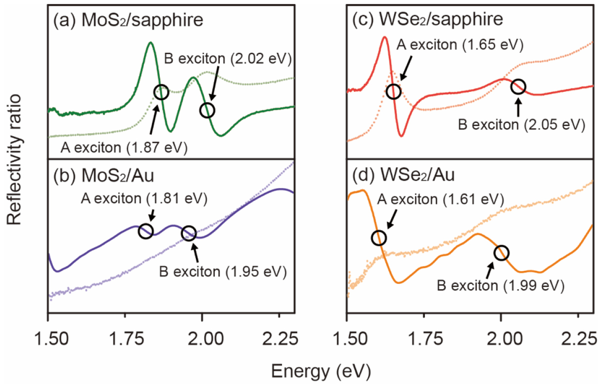
To obtain Eb,exc, we also need to know the fundamental exciton transition energy of the TMDCs on the metallic and dielectric supports. At room temperature, the absorptive optical response close to the band edges in TMDCs is known to be strongly dominated by excitons, with only a faint contribution due to trions at slightly lower energies than the main exciton transition [54]. In particular, MoS2 and WSe2 exhibit two prominent excitonic features, termed A and B excitons, which stem from transitions at the K-point. The energy difference between A and B is caused by valence band splitting due to spin–orbit coupling [19]. In the following, we focus on the energy range of these A and B resonances and do not consider higher excitations. To obtain the excitonic transition energies, Eexc, we performed reflectance measurements as shown in figure 4, which displays measured data (dashed lines) and their first derivative (solid lines) to clearly identify the transition energies, particularly on Au, where the features are less pronounced. In figures 4(a) and (c), MoS2 and WSe2 on sapphire show the known excitonic transitions due to the strong light–matter interaction associated with van Hove singularities of their density of states [55]. The respective peak maxima yield 1.87 eV and 2.02 eV for MoS2, and 1.65 eV and 2.05 eV for WSe2 of the A and B excitons, respectively. These values of Eexc are in agreement with earlier results obtained for these TMDCs on insulators, such as sapphire, fused silica, and quartz [32, 56, 57]. Additionally performed PL measurements showed a peak maximum at the reported literature values corresponding to the exciton transition in these TMDCs (see SI) [58, 59].

Figure 4. Measured reflectance spectra (dashed lines) and the first derivative of the reflectance spectra (solid lines) [ ] of (a) MoS2 on sapphire, (b) MoS2 on Au, (c) WSe2 on sapphire and (d) WSe2 on Au. The circles denote the energy position of the A and B exciton.
Download figure:
Standard image High-resolution imageThe reflectance spectra of MoS2 and WSe2 monolayers on Au show less pronounced excitonic peaks due to the strong background, as evident from figures 4(b) and (d). The proximity of the metal, and possibly a small charge transfer as noted above, substantially influence the optical signature. Yet remarkably, the exciton energies barely change, also in agreement with the result of Mertens et al [60]. Accordingly, the transition energies of the A and B excitons, respectively, are determined to be 1.81 eV and 1.95 eV for MoS2/Au, and 1.61 eV and 1.99 eV for WSe2/Au.
The most important parameters obtained in this study and the energy level diagrams at the K-point, including the sample work function, are summarized in figure 5 (further details are contained in the SI). On sapphire, the directly determined Eb,exc amounts to 240 meV for both MoS2 and WSe2, while on Au it is strongly reduced to be 90 meV for MoS2 and 150 meV for WSe2, respectively. This observed reduction of Eb,exc is in line with previously suggested models [20, 30, 61]. Notably, theoretical calculations of Eb,exc for MoS2 and WSe2 predicted values of 540 meV–770 meV and 740 meV, respectively [3, 62], which is more than ca. 300 meV higher than determined in the present study. This difference is due to the fact that the calculations did not include any dielectric medium in proximity to the TMDCs, although this is predominantly the case in device structures. In addition, combined experimental and theoretical studies also demonstrated negligible change in exciton binding energy under strain [62, 63] This implies that strong changes in the band structure (and most specifically change of Eg) due to strain should lead to the same changes in Eexc. As this is not observed, we can rule out the effect of strain in the observed changes in Eg and in Eb,exc reduction as determined in the present study. In other previous studies, optical measurements for MoS2 and WSe2 supported on insulator substrates were analyzed using the hydrogenic Rydberg model, which gave indirect estimations of Eb,exc with values in the range of 280 meV–440 meV (MoS2) and 240 meV–370 meV (WSe2), in fair agreement with our values from a direct determination [32, 64–66]. Unfortunately, Eb,exc values derived with this model for these two TMDCs on metal substrates are not available and preclude further comparison.

Figure 5. Energy level diagram of MoS2/sapphire, MoS2/Au, WSe2/sapphire, and WSe2/Au. All values are given at the K-point.
Download figure:
Standard image High-resolution image
Regarding the energy levels, MoS2 on sapphire exhibits apparent n-type character and a high ionization energy (IE) of 6.26 eV, which agrees with the results from Berg et al [38]. The IE of MoS2/Au, WSe2/sapphire, and WSe2/Au are found be 6.20 eV, 5.09 eV, and 5.40 eV, respectively. However, the IE values should be used with care, as the TMDCs monolayers did not cover the substrates completely, and the work function (used to determine IE) is an area-average. We suggest considering an error margin of up to 0.5 eV. From the energy level diagrams in figure 5 we can see that substantial energy barriers for the injection of both electrons and holes from Au into MoS2 and WSe2 exist, highlighting the need to engineer ways for improved carrier injection from such electrodes. Until now, several 2D TMDCs energy level diagrams derived from photoemission are available, however only from measurements at the Γ point [67–69]. As the actual VBM and CBM minima of the two materials investigated here occur at the K-point, such level diagrams over-estimate injection barriers. Consequently, the diagrams of figure 5 based on ARPES and ARIPES measurements at the K-point are more relevant for understanding the characteristics of TMDCs-based devices.
To summarize, we directly determined Eb,exc from Eg and Eexc measurements for MoS2 and WSe2 monolayers on sapphire and Au substrates. With ARPES and ARIPES measurements, we provide experimental evidence that the K-point features the minimum and direct band gap. The evaluated Eg and Eb,exc values are 2.11 eV and 240 meV for MoS2/sapphire and 1.89 eV and 240 meV for WSe2/sapphire, respectively. Owing to improved dielectric screening and possibly a small charge transfer when placing the monolayers on Au, a significant decrease in Eg by 0.21 eV and 0.14 eV was measured for MoS2 and WSe2, respectively. Notably, the exciton energy is barely affected by the metal substrate in comparison to the insulating sapphire. Consequently, on Au we observe a huge reduction of Eb,exc for MoS2 and WSe2 by 150 meV and 100 meV, respectively. As a result, Eb,exc determined to be 90 meV for MoS2 on Au and 140 meV for WSe2 on Au, respectively. Accordingly, the present results serve as a benchmark in order to evaluate models to derive the exciton binding energies in alternative ways, e.g. the hydrogenic Rydberg model and its extensions, particularly for the case of coupling TMDCs with metallic substrates. In terms of energy levels, MoS2/Au shows a more p-type character as compared to the apparent n-type one on sapphire. In contrast, WSe2 appears almost intrinsic on both substrates. The present results help to rationalize the excitonic properties of 2D TMDCs in different dielectric environments and will be useful for designing optoelectronic devices based on this class of intriguing materials.
Acknowledgment
This work was supported by the DFG (SFB951 and AM 419/1-1).
Author contributions
SP wrote the manuscript; collected and analyzed all of the data presented in this manuscript under the supervision of EJLK and NK; NM and SB performed and analyzed the optical experiments. SP and TS performed ARPES, ARIPES experiments and DFT calculations. PA revised the manuscript. AH, AA and LL prepared the TMDC samples for measurement. All authors participated in the discussion and interpretation of the results and commented on the manuscript.
Notes
The authors declare no competing financial interest.