Abstract
The evolution of grapheneʼs electrical transport properties due to processing with the polymer polymethyl methacrylate (PMMA) and heat are examined in this study. The use of stencil (shadow mask) lithography enables fabrication of graphene devices without the usage of polymers, chemicals or heat, allowing us to measure the evolution of the electrical transport properties during individual processing steps from the initial as-exfoliated to the PMMA-processed graphene. Heating generally promotes the conformation of graphene to SiO2 and is found to play a major role for the electrical properties of graphene while PMMA residues are found to be surprisingly benign. In accordance with this picture, graphene devices with initially high carrier mobility tend to suffer a decrease in carrier mobility, while in contrast an improvement is observed for low carrier mobility devices. We explain this by noting that flakes conforming poorly to the substrate will have a higher carrier mobility which will however be reduced as heat treatment enhance the conformation. We finally show the electrical properties of graphene to be reversible upon heat treatments in air up to 200 °C.
Export citation and abstract BibTeX RIS

Content from this work may be used under the terms of the Creative Commons Attribution 3.0 licence. Any further distribution of this work must maintain attribution to the author(s) and the title of the work, journal citation and DOI.
1. Introduction
Grapheneʼs electronic characteristics play an important role for a variety of applications such as transistors and integrated electronic circuits [1–3], sensors [4, 5] and large-area transparent electrodes [6]. Graphene is commonly produced either by mechanical exfoliation from graphite or by chemical vapour deposition (CVD). In particular, CVD graphene is a promising route towards production of high quality graphene for electronic applications. The graphene is typically grown on a catalyst substrate, from which it is transferred to an insulating substrate and patterned by lithographic means. Polymethyl methacrylate (PMMA) is used for the majority of published transfer techniques [7–9] and electron-beam lithography (EBL) patterning processes such as the fabrication of electrodes [10, 11], and nanopatterning of the graphene to manipulate the electronic properties [12–14].
On the one hand, PMMA is cheap, versatile, has good mechanical properties and is an excellent high-resolution electron-beam resist. On the other hand PMMA invariably leaves residues on graphene after having been in direct contact. This is considered to be a serious problem for device fabrication, as PMMA residues are notoriously difficult to remove [15, 16]. In addition, processing with PMMA typically implies temperature annealing steps in controlled atmospheres and/or baking in air [17–19]. As graphene can be viewed as a material consisting entirely of surface atoms, any one of such individual processing steps could considerably affect the electrical performance of graphene devices. In order to study this systematically, it is important to fabricate devices in a way that preserves the electrical properties of the initial as-exfoliated graphene as much as possible. To do so, electrical contacts can be fabricated by the use of mechanical shadow masks (stencil masks) [20], where contact with polymers, chemicals and heat is avoided entirely and the graphene channel is therefore left in a pristine state. We emphasize that the impact of PMMA processing on the electrical characteristics of graphene cannot be assessed with devices contacted by any conventional lithographic techniques, as such devices are already altered by the contacting processing steps.
Here we deposit metallic contacts to micromechanically exfoliated graphene flakes using the cross-bars in commercially available TEM grids as a shadow mask [21–24]. We use this clean device fabrication approach to systematically test the effect of typical PMMA related processing steps on the electrical properties of graphene. We measure the electrical properties of the devices after each individual processing step, thus evaluating the evolution from the initial as-exfoliated graphene to the PMMA processed graphene. We find that heat processes are mostly responsible for the degradation of the electrical performance of graphene devices rather than PMMA residues.
2. Methods
Stencil devices were fabricated on highly doped (1–2  ) silicon wafers with a 300 nm silicon dioxide layer. The oxide was plasma-cleaned prior to the mechanical exfoliation of graphene to avoid trapping of organic residues below the graphene. The plasma clean was performed with a power of 400 W and a gas flow of 200 sccm O2 and 50 sccm N2. The graphene was subsequently located and identified by optical contrast [25] and Raman spectroscopy [26]. Stencil contacts were fabricated with a TEM grid based shadow mask aligned to the graphene flake under an optical microscope. E-beam evaporation of a 50 nm thick gold layer was used to define the source and drain electrodes. A schematic drawing of the device fabrication is seen in figure 1 along with an optical image of a typical stencil device.
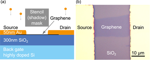
Figure 1. (a) Schematic drawing of the graphene stencil device fabrication. (b) Optical image of a graphene stencil device (the contrast of the image has been enhanced).
Download figure:
Standard image High-resolution imageDevices were electrically characterized in a controlled atmosphere stage (Linkam LTS600P) equipped with electrical feedthroughs and a built-in heating element. The source–drain resistance was measured as a function of applied gate voltage, and all electrical measurements were performed at room temperature in a nitrogen atmosphere (AGA, nitrogen 5.0, purity of 99.999%).
Electrical measurements were undertaken after each of the following PMMA processing steps (see figure 2): (1) stencil device fabrication. (2) 30 min temperature anneal at 250  C in a nitrogen atmosphere (TA). (3) Ventilation of the device chamber with ambient air. (4) Baking at 200
  C in air for 30 min (both time and temperature are typically used in EBL fabrication as a dehydration bake [17]). (5) Applying, curing and removal of a 40 nm thick PMMA layer. The PMMA was spun and cured on the devices using a temperature ramp typical for high resolution EBL [18]. The curing process starts with a one hour temperature ramp from room temperature to 120
  C. The devices were then held at this temperature for three hours, before being ramped to 180
  C over one hour, and held at this temperature for six hours, followed by a ramp back to room temperature over two hours. The curing process was carried out in ambient conditions. The PMMA was removed in 40
  C acetone and the devices were rinsed in isopropyl alcohol before a N2 dry. After these process steps PMMA residues were clearly present on the graphene, as seen in the SEM image in supplementary figure S2. (6) Temperature annealing of the devices as in step 2, which is a common step carried out to enhance the electrical properties of graphene devices [10, 15, 27, 28].
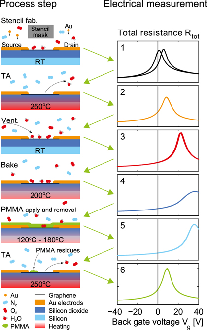
Figure 2. Outline of the process steps and the gate voltage sweeps performed after each step on the representative device (D1). All y-axes are scaled from 0 to 4.5 kΩ and all electrical measurements are performed at room temperature in a N2 atmosphere at ambient pressure.
Download figure:
Standard image High-resolution imageRegarding the evolution of the electrical measurements, our key figures of merit (FoM) for this study are the average position of the charge neutrality point  , the gate voltage hysteresis
  and the mobility, which is represented by the hole carrier mobility
  .
.  and
and  are found directly from the gate voltage sweep. The value for
  is more challenging to determine in two-terminal graphene devices due to the contact resistance of the source and drain contacts RC. The model presented by Kim et al [29] was applied to the data in order to extract
  (see supplementary information for details). This approach assumes that the contact resistance has an insignificant dependence of the gate voltage, which is disputed by [10, 30]. In our case, the relatively large device length (
 μm) and a low contact resistances extracted from the data, indicate that this possible dependence does not affect the conclusions of our study. We note that in this case, the usage of four point stencil devices would eliminate RC, however, could also make interpretation of our results more difficult, as the metal of the four point voltage contacts would introduce doping into the graphene channel [31].
3. Main results and discussion
The changes of the three key FoM,  ,
,  and
and  , of the graphene along the six processing steps are plotted in figure 3. The resistance versus gate voltage for device D1 is shown in figure 2, and for device D2–D5 in supplementary figure S3.
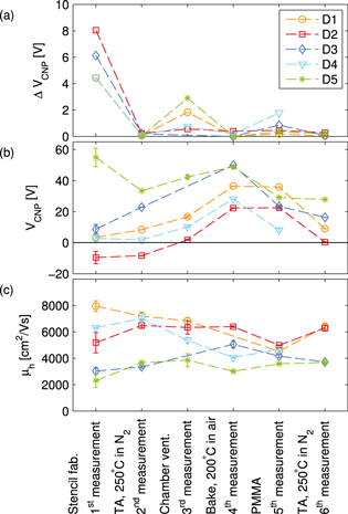
Figure 3. The evolution of the gate voltage hysteresis  the doping
  and the hole mobility
  throughout the six selected PMMA processing steps, for the five studied devices. All electrical measurements are performed at room temperature in a N2 atmosphere at ambient pressure.
Download figure:
Standard image High-resolution image3.1. Hysteresis
The gate voltage hysteresis,  in figure 3(a), is largest at the measurements of the initial as-fabricated devices (step 1). A smaller hysteresis is also present after ventilation of the chamber (step 3), and after PMMA processing (step 5). Thermal annealing in a N2 atmosphere and baking in air (step 2, 4 and 6) considerably reduced
  .
.
Hysteresis in graphene devices is commonly ascribed to adsorbed water molecules and other species [10, 22]. In our case the large initial hysteresis could be due to presence of water below as well as on top of the graphene after fabrication [32]. The amount of water below the graphene and thereby the hysteresis can be minimized with the use of a hydrophobic substrate [28, 33–35]. After the first TA water will mainly be re-adsorb on top of the graphene, leading to a smaller increase hysteresis when again exposing to air. Another possibility is that the first annealing step adsorbs a considerable amount of non-water species that contribute to the higher initial hysteresis, and which do not all re-adsorb upon air exposure.
3.2. Doping and mobility
The evolution of  , figure 3(b), follows the same trend for all the devices. An average increase of
  across the devices is observed after ventilation of the chamber (step 3), followed by an average increase of
  after bake in ambient air (step 4), and an average decrease of
  after the final TA in nitrogen (step 6).
A large variation of the initial  was observed in the as-fabricated devices (step 1), which corresponds to a spread in charge carrier concentration of
  −2 among the measured devices. Similar variations of n on exfoliated non-processed graphene on SiO2 have been extracted via Raman spectroscopy [36–38]. After the sequence of PMMA processing steps, involving chemicals and heating, p-type doping with a smaller variation is measured on all the devices.
The hole carrier mobility  is shown in figure 3(c). Similar to
  a large initial spread of
  (from 2000 cm2 Vs−1 to 8000 cm2 Vs−1) was observed in the as-fabricated devices, which however decreased with the number processing steps.
As explained in detail below, we attribute both the p-doping and carrier mobility behaviour to an interplay between particle contamination and the mechanical conformation of the graphene to the substrate due to processing steps: in particular those involving heating.
On one hand it is known that the presence of molecules on graphene strongly affect the charge carrier concentration of the monolayer. In particular O2 molecules together with H2O molecules lead to strong hole doping of graphene [21, 33, 39]. On the other hand, the mobility is influenced by the substrate in two ways. First, contact with SiO2 leads to polar optical phonon scattering [40, 41]. Second, the higher the conformation of the graphene to the corrugated SiO2 substrate, the larger is the reactivity of the graphene towards oxygen molecules [21]. A higher conformation to the SiO2 substrate would therefore lead to an increase of the amount of impurities on the graphene, which in turn reduces the carrier mobility through long-range Coulomb scattering [42] and increases the doping level of the graphene [21, 42]. In agreement with this picture, graphene has been reported to be far more smooth on exfoliated hexagonal boron nitride substrates than on SiO2, without the distinct p-doping upon exposure to air [43–45]. Furthermore, according to [21, 44], graphene conforms more to the substrate when it is heated up. To confirm this for our samples, we carried out line scans across graphene-SiO2 interfaces using atomic force microscopy (AFM), and compared directly regions before and after annealing, see figure 4. Before annealing (figure 4(a) and (c)) the graphene flake appears qualitatively different from the SiO2 surface, with clear lateral streaks, as also reported in [36], yet with significantly less vertical corrugation. We note that the graphene flake before annealing appears to conform to the SiO2 near the edges. After annealing (figure 4(b) and (d)) the graphene and SiO2 surface appear strikingly similar except for a vertical offset. The scale of vertical corrugations on graphene and SiO2 is very similar after annealing. Care was taken to perform the line scans in the exact same position, and the curves before (blue) and after (black) annealing show nearly the same features on the SiO2.
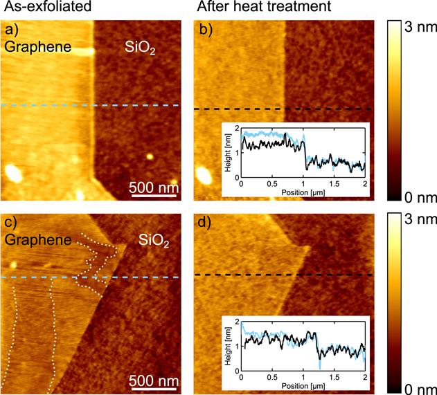
Figure 4. AFM scans of two graphene flakes before (a) and (c) and after (b) and (d) heat treatment. The line scans were extracted in approximately the same vertical position, which is apparent from the insets, showing before and after annealing curves as blue and black color, respectively. Before annealing the graphene flakes show extended ripple-like texture, very different from the SiO2 surface, and overall smaller vertical corrugations from the oxide. After annealing the surfaces clearly resemble each other, and have similar surface roughness. The white dotted line in panel (c) marks areas with pronounced micrometer sized corrugations.
Download figure:
Standard image High-resolution imageIn our measurements, after the first TA in step 2, as-fabricated graphene conforms more to the SiO2 surface, which does indeed support our interpretation of the observed p-doping in all our devices upon ventilating the chamber (step 3). This behaviour was consistently observed in all devices studied here, as well as any other devices investigated prior to this study (>20). Furthermore, we also confirmed this rapid doping by Raman spectra obtained through a glass window in the environmentally controlled measurement chamber, while slowly exposing a temperature annealed sample to air, see supplementary figure S4. The devices are also observed to become further p-doped after the bake in air at step 4. The possibility of recovering the original FoM of graphene upon baking in air is investigated further in section 3.3.
The same explanation for the doping behaviour also holds for the observed changes of  . The devices with a high initial
  (D1 and D4) would have a lower degree of conformation to the substrate and following the argument presented above, a lower level of impurities on the graphene surface and lower coupling to the phonons of the SiO2. After the TAs and baking in air are performed, the conformation of the graphene to the SiO2 is increased, and the level of charged impurities is consequently enhanced. This leads to phonon and Coulomb scattering and a decrease in the value of
  . In contrast, devices with an initially high conformation of the graphene to the SiO2 would have a low initial
  . This latter case reproduces the commonly observed electrical features from conventionally contacted devices, where graphene already is conformed during the lithographic steps and any annealing process carried out afterwards mainly improves the performance of the devices [19]. We observe this trend in D3 and D5 after the corresponding annealing processes. We also note that after the full sequence of processing steps, our devices have a more uniform value of
  , similar to devices contacted using conventional lithography [10]. In addition, the carrier mobility of the devices is not consistently modified after the PMMA exposure step, which shows that the sole presence of PMMA on top of graphene cannot alone be held responsible for degrading the mobility of graphene on SiO2, at least not for devices in this quality range.
Finally, we note that the devices only after all the PMMA processing steps have the typical characteristics of Coulomb scattering [42], where the devices with lowest doping have the highest mobility and vice versa. This trend was not observed in the as-fabricated graphene devices, due to the interplay between the variation in the degree of conformation to the SiO2 substrate and the amount of impurities on the monolayer. Our work elucidates the evolution of electrical characteristics evolution during the chemical and heating typical from PMMA processing, and reconciles optical Raman measurements of unprocessed graphene [36, 40, 46] and electrical measurements on devices contacted by standard lithographic techniques [10, 42].
3.3. Baking under ambient conditions
Stencil devices are in this section used to test the possibility of baking graphene in air without permanently diminishing its electrical properties. Baking in air on hotplates or in ovens is commonly performed in cleanroom processing as a dehydration bake to evaporate water from the surface of the wafer prior to EBL- or photo-resist application [17]. Baking of graphene in air at 200  C turned out to contribute to the p-doping during the PMMA processing steps (see section 3.2), this step was therefore investigated further to determine the baking temperature up to which doping and mobility degradation are still reversible by temperature annealing.
The enhancement of the electrical properties of graphene by temperature annealing in vacuum have shown to increase with annealing temperature until a turnaround temperature, after which the electrical properties start to diminish [47]. We observe the same trend for temperature anneals in N2 on the stencil samples. The annealing temperature is therefore fixed to obtain the same values of doping and mobility after repeating TA on graphene devices. All temperature anneals (unless otherwise stated) lasted 30 min and were performed at 250  C in N2. The first temperature anneal immediately leads an enhanced conformation of the graphene to the substrate before baking in air and thus increasing the reactivity with air species [21, 44, 48].
The stencil devices were first measured in their initial as-fabricated state (measurement 1 in figure 5), followed by temperature annealing to determine the baseline electrical characteristics of the devices (measurement 2). The devices were then repeatedly baked in ambient air at increasing temperatures from 100 to 300  C in steps of 25
  C with a TA in between each bake. Electrical measurements were performed after each bake/TA (measurement 3–20). All measurements were carried out in N2 after cooling the devices down to room temperature. An anneal at 300
  C in N2 was furthermore performed after the final bake in air at 300
  C, however the increased temperature of the TA could not reverse the degeneration of the graphene FoM (measurement 21). Figure 5 shows the mobilities and doping levels for two devices (D6 and D7) at measurement 1–21.

Figure 5. The evolution of the charge carrier mobility (left y-axis and ○) and doping level (right y-axis and  ) of two stencil devices, that are alternated between bakes in air and temperature annealing in nitrogen. All the electrical measurements are performed at room temperature in a N2 atmosphere at ambient pressure. Data from one more device is presented in supplementary figure S5.
Download figure:
Standard image High-resolution image
The mobility and doping for the two devices were recovered after the bakes in air until 200  C by a TA. Raman spectra were obtained from these devices before any processing and after baking up to 300
  C in air (supplementary figure S6). A shift in the G peak position from
  to
to  and a reduction in the 2D to G intensity ratio were observed; which corresponds to a considerable increase of the doping level according to [49]. A similar result was observed previously using Raman spectroscopy [48]. The observed irreversible doping can be due to an increased reactivity with O2 [48] and/or induced carbon contamination [27] as a result of the high baking temperatures, as previously pointed out.
These results indicate that graphene interact with air in an irreversible and undesirable manner when baked at temperature above 200  C in air, and such temperatures should therefore be avoided in graphene fabrication processes.
4. Conclusions
The use of stencil lithography combined with a systematic approach makes it possible to distinguish the impact of different processing steps on the electrical properties of graphene. We showed the evolution of hysteresis, doping and mobility of pristine contacted graphene through a sequence of PMMA processing steps. The initial hysteresis of the as-exfoliated graphene was nearly eliminated by temperature annealing at 250  C in N2, and re-appeared in a reduced form upon exposure to air. A large initial variability of both the doping levels and hole carrier mobilities of the as-exfoliated graphene were observed and attributed to differences in the initial conformation to the SiO2 substrate and particle contamination of the graphene. The variation of these values between the different devices is decreased during the PMMA processing steps. The devices were p-doped after the sequence of steps, and the data supports the notion that this p-doping is due to corrugation of the graphene rather than the actual PMMA residues on the graphene surface. We found that these presumably uncorrugated graphene devices are subject to a mobility decrease during annealing processes in contrast to the normal case of graphene partly or fully conforming to the substrate even before the first measurement is carried out. Stencil fabrication seems like an ideal approach towards achieving the superior carrier mobility expected of a semi-suspended, quasi-stable state even on materials such as SiO2, while avoiding the collapse caused by heat treatment or other processing. Furthermore, the electrical properties of devices baked in air at temperatures below 200
  C were shown to be recoverable by temperature annealing. The observations here thus reconcile published Raman data of as-exfoliated graphene and electrical measurement on conventional devices. Our work shows that the stencil device approach is a cheap, fast, simple, yet powerful platform for the systematic optimization and fault-finding invariably needed for fundamental research as well as commercialization of graphene-based electronic devices.
Acknowledgements
We acknowledge financial support from the EC Graphene FET Flagship, the Center for Nanostructured Graphene (CNG, DNRF58) funded by the Danish National Research Foundation and the Danish Council for Independent Research (FTP Gravox). We furthermore thank Bjarke Sørensen Jessen for the software Graphene Hunter for automated identification of graphene flakes.