
Abstract
TM surface plasmon (SP) characteristics of a four-layer structure, consisting of air as the superstrate, a monolayer of graphene, a dielectric buffer layer and metal as the substrate are analyzed at sub-THz frequencies. TM SPs in such case are represented by metal-like and graphene-like branches. For small frequencies the metal-like plasmon splits up into two branches depending on the graphene electron concentration; one of the branches goes into cutoff at the point where the branch features Brewster-type characteristics. Graphene-like plasmon modes are converted into short-range modes for small buffer thicknesses. Brewster-type SP modes can be effectively modulated in the vicinity of their cutoff thicknesses by means of the graphene electron concentration.
Export citation and abstract BibTeX RIS

Content from this work may be used under the terms of the Creative Commons Attribution 3.0 licence. Any further distribution of this work must maintain attribution to the author(s) and the title of the work, journal citation and DOI.
1. Introduction
Electronic, optical and mechanical properties of graphene were extensively studied after the appearance of the first publication devoted to experimental investigations of graphene [1]; results of these studies were widely published [2–4]. Free carriers in graphene can be created either by doping or by field effects. A graphene electron gas of high mobility forms an ideal two dimensional sheet [1]. The optical surface conductivity of a graphene monolayer was studied in a wide range of frequencies, from the terahertz to the visible range [2, 5–8]. Electromagnetic wave (EMW) propagation in structures containing graphene layers was investigated in a number of publications [9–12] and various perspective applications for graphene in photonics and optoelectronics have been discussed [13]. Special attention was paid to plasmons supported by graphene layers and which are tunable by a gate voltage. Perspective applications of graphene plasmons in nanophotonics due to their high confinement around the graphene layer have been discussed in many papers [14–23].
In spite of the fact that graphene plasmons were investigated in a number of structures containing a few graphene monolayers or graphene bilayers, the case of graphene plasmons coupled with other types of structure modes (surface metal-plasmon or waveguide modes) has not been thoroughly examined. The coupling of graphene plasmons with surface metal plasmons in a structure containing a graphene layer and metal substrate separated by an air gap was studied [24]: the solution of the coupled plasmon mode shows a linear dispersion behavior in a specific parameter range.
In this article we analyze the propagation characteristics of TM coupled modes in a structure containing a metal substrate, dielectric buffer layer, a monolayer of graphene, and air as the superstrate.
The article is divided into two parts. In the first part, the dispersion equation for TM eigenmodes and some of its approximate solutions are given on the basis of Maxwell's equations solution. In the second part, dispersion characteristics of coupled graphene-metal plasmons are analyzed on the basis of numerical solutions of the dispersion equation for sub-THz frequencies. The results are summarized in the conclusions.
2. Dispersion equation for the coupled graphene-metal surface plasmons (MSPs) in four-layered structure
We consider the propagation of TM-polarized EMWs along the Z direction in the structure shown in figure 1; magnetic field of TM-polarized EMW is directed along X axis and electric field vector of TM-polarized EMW is parallel to (Y, Z) plane, the magnetic and electric field component respectively can be written as: H = (Hx, 0, 0), and E = (0, Ey, Ez). The structure of figure 1 consists of a metal substrate with relative dielectric permittivity  a buffer layer of thickness d2 and relative dielectric permittivity
  a graphene monolayer created on the buffer layer surface y = 0 (Y-axis is orthogonal to the multi-layer structure) and air as the lossless superstrate medium behind the graphene layer with relative dielectric permittivity
  .
.
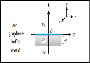
Figure 1. Schematic view of the multi-layer structure, which consists of air/graphene/buffer layer(SiO2)/metal (gold).
Download figure:
Standard image High-resolution imageThe standard electrodynamic boundary conditions represented by the continuity of the electric field tangential component at the interfaces y = 0, y = −d2 and by the continuity of the magnetic field tangential component at the interface y = −d2 are used to calculate the EMW propagation in the structure of figure 1. The boundary condition for the tangential component of the magnetic field at y = 0 is modified by the presence of the monolayer of graphene, which features a surface electron concentration ns and a surface conductivity  In the SI units, the boundary condition can be written down as follows:

where  and
and  are the tangential components of the magnetic field in the superstrate and the buffer layer, respectively;
  is the amplitude of the tangential component of the electric field at y = 0.
Straightforward calculations for the TM eigenmodes lead to the spatial distribution of the magnetic field amplitude given by equations (2a) and (2c) and to the dispersion equation (3): y > 0:

−d2 < y < 0:

y < −d2:


where: 


 for j = 1, 2, 3,
  where q is the propagation constant in z direction,
  is the electromagnetic wavenumber in vacuum, ω is the EMW angular frequency,
  where c is the EMW speed in vacuum,
  and μ0 are permittivity and permeability of vacuum.
Throughout the paper we ignore the spatial dispersion of graphene conductivity, suggesting that  the Fermi velocity is
  [25], however temporal dispersion of graphene conductivity is taken into account therefore
  We use equation (4a) for graphene's conductivity
  consisting of intraband
  and interband
  contributions [2]:

where


 are the electron energy and Fermi level energy, respectively,
  kB is Boltzmann constant, t is temperature in Kelvin, e is the electron charge and
  is the electron relaxation time;
  and f(
 ) is the electron distribution function.
Dependence of Fermi level energy EF (from now on this energy is denoted as Fermi level) versus graphene surface electron concentration  and temperature t is defined by the following integral equation:

Interband transitions become more important for higher optical frequencies and lower Fermi levels. At room temperature, and low terahertz frequencies f < 30 THz, intraband transitions give the largest contribution to the optical conductivity of the graphene monolayer for EF > 0.05 eV (EMW frequency is denoted as f, in contrast to electron distribution function which is denoted as f()).
Equation (3) was derived in [26] although the coupling of MSPs and surface carrier plasmons created by a two dimensional surface charge  embedded in the interface y = 0 had not been studied.
For a very wide buffer layer thickness when  equation (3) reduces to the dispersion equations of both decoupled TM MSPs (equation (6)) and TM graphene plasmons (equation (7), see also [7, 12, 26]):


Rewriting equation (6) leads to the well-known dispersion relation for MSPs [27] given by equation (8):

Equation (7) is described by the 4th power equation for the q2 value and its general solutions are too cumbersome to write them down. However, the solution is considerably simplified for the case  when the dispersion relation for graphene plasmons can be written down as follows [7]:

Taking into account only the intraband contribution to graphene's optical conductivity given by equation (4b) for  equation (3) is reduced to equation (10) for
  (j = 1, 2, 3),
 (ωp is the metal electron plasma frequency):
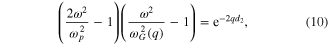
where ![${{\omega }_{G}}\left( q \right)=\sqrt{\frac{4T{{e}^{2}}q}{{{\hbar }^{2}}}\;{\rm ln} \left[ 2{\rm cosh} \left( {{E}_{F}}/2T \right) \right]}$](https://content.cld.iop.org/journals/2040-8986/17/4/045003/revision1/jopt510881ieqn36.gif) is the graphene plasmon frequency defined by equation (9). Equation (10) is coincident with equation (22) derived in [24]; the equation describes frequencies of coupled metal-graphene plasmons for
is the graphene plasmon frequency defined by equation (9). Equation (10) is coincident with equation (22) derived in [24]; the equation describes frequencies of coupled metal-graphene plasmons for  when the plasmon absorption is totally neglected. However, this equation is valid only for large propagation constant values when the conditions
  are fulfilled and these inequalities are not fulfilled for long-range modes of low terahertz frequencies propagating in the structure of figure 1 with material parameters under study (refer to the graphs plotted in figure 2). In this case it is necessary to solve equation (3) to find out the dispersion of the coupled modes. The terms long/short-range modes are used to define the amount of mode damping: for long-range or short-range modes the propagation length is respectively larger or smaller than the mode's wavelength.
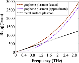
Figure 2. Dependences of the propagation constant q real parts of decoupled MSP and GSP versus plasmon frequencies for wide buffer layer thickness at Fermi level EF = 0.5 eV; exact and approximate dispersion dependences for GSP, and an exact MSP dispersion dependences.
Download figure:
Standard image High-resolution image3. Results of numerical calculations and discussion
Numerical calculations were performed for the structure of figure 1 with the following material parameters for the different layers: the relative dielectric permittivity of air  for the buffer layer we consider SiO2 with
  valid for EMW frequency
  [28], and finally for the metal we used Au. Frequency dependent dielectric relative permittivity
  of Au is described by Drude model with plasma and damping frequencies taken from [29]. The optical conductivity of graphene depends on the electron relaxation time
  whereby the
  value is evaluated from the DC mobility
  according to the relation
 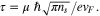 As the mobility values measured in [1] varied between (0.3–1) × 104 cm2 V−1 s−1 at room temperature we suggest
  in our calculations.
Mathematically speaking, equation (3) can yield a large set of complex valued wave vector solutions, leading to many branches in the dispersion spectrum. This solution set can be divided into waveguide mode and surface plasmon (SP) like solutions. The analyses of the latter type of solutions will be the topic of this paper. From these SP mode solutions, we discuss only the bound modes which are the most relevant in the perspective of applications. Such modes feature positive values of the real and imaginary parts of the propagation constant with small (short range) or large (long range) propagation lengths. For further classification of the SP mode branches we first assume an infinite thick buffer, such that one can define purely decoupled but Fermi level dependent graphene surface plasmons (GSP) and MSP solutions. The MSP solution exist over the full considered Fermi level range (0–0.5 eV), however the GSP do not.
The dependences of the real parts of the propagation constant of the decoupled MSP and GSP modes on the plasmon frequencies for EF = 0.5 eV are depicted in figure 2 versus.
The pure MSP results from equation (8), which even approximates to  for low THz frequencies. The pure GSP exists in the three-layer system air/graphene/buffer: equation (7) yields the exact solution and equation (9) for
 yields an approximate solution.
The approximate solution of equation (9) leads to considerable errors over the whole considered frequency band. It is also seen that the difference of decoupled MSP and GSP propagation constant vanishes for low THz and GHz frequencies. Hence we may expect stronger coupling effects in this frequency range. All subsequent numerical calculations are mainly performed in the strong coupling regime for f = 0.3 THz.
The dispersion dependence of decoupled GSP on graphene's electron Fermi energy level is shown in figure 3 for the EMW frequency f = 0.3 THz. From figure 3 one can observe that the decoupled GSP is represented by a long-range mode only for  when
when  and the GSP propagates at least one wavelength.
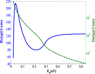
Figure 3. Dependences of GSP wavector for the three-layer structure: air/graphene/SiO2 versus Fermi level for f = 0.3 THz: the real part (left), and the logarithmic scale of the imaginary part (right) of the GSP propagation constant.
Download figure:
Standard image High-resolution imageIt is obvious that for a thinner buffer layer decoupled plasmon dispersion dependences will modify. In the extreme case of a very thin buffer layer when  the only long-range solution of equation (3) exists and this is represented by the MSP for the two-layer superstrate/metal structure. This solution is very close to that given by equation (8) with the substitution
 although slightly modified due to the presence of the monolayer graphene. The long-range SP tends to become the surface metal plasmon of the three-layer structure superstrate/buffer/metal in the case of small electron concentrations in graphene. Increasing the graphene electron concentration leads to a considerable modification of the coupled SP spectrum.
We classify coupled SPs as metal-like surface plasmons (MLSP) and graphene-like surface (GLSP) plasmons depending on their behavior for  .
.
At this juncture the dependences of coupled plasmon modes on the buffer thickness and the Fermi level EF in the graphene will be elaborated.
Dependences of MLSP propagation constant values versus buffer thickness for different Fermi levels are shown in figure 4. All the mode propagation constant values converge to the decoupled MSP propagation constant  for
for  .
.

Figure 4. Dependences of MLSP propagation constant q versus buffer layer thickness for f = 0.3 THz at different Fermi level values EF (a) real part, (b) imaginary part.
Download figure:
Standard image High-resolution imageIt was observed that the imaginary part of the mode propagation constant increases with the Fermi level, reaching exactly the maximum value 29.46 cm−1 for d2 = 127 μm at EF = 0.178 eV.
For larger Fermi levels, the MLSP spectrum is considerably modified: as illustrated in figure 5.

Figure 5. Dependences of the propagation constant values q for continuous MLSP (solid line) and cutoff MLSP (dot line) branches versus buffer layer thickness for f = 0.3 THz at different Fermi level values EF (a) real part, (b) imaginary part, of the propagation constant.
Download figure:
Standard image High-resolution imageThe MLSP splits up into two mode branches. One of them exists within the whole range of buffer thicknesses and this solution is called the continuous MLSP branch, the other MLSP solution exists only for buffer thicknesses smaller than the cutoff thickness d2c and this is called the cutoff MLSP mode. For  the propagation constant solution converges to
  and it converts from long-range solution to a short-range solution for buffer layer thinner than
  On the other hand the cutoff MLSP branch exists only for a buffer layer thicknesses thinner than
  (
( for
for  and for
  the propagation constant solution tends towards
  also the imaginary part of the propagation constant vanishes at the cutoff thickness d2c. Furthermore, the cutoff MLSP branch converts from the bound type mode for d2 < d2c to the growing type mode for d2 > d2c and this branch is represented by an incident plane wave without any reflection for d2 = d2c. These kinds of modes are called Brewster-type modes [30]. The whole incident wave is actually absorbed inside the structure [31, 32]. The propagation constant values real parts
  at the cutoff conditions for TM modes can be found from the solution of equation (11):
where 
Buffer layer thicknesses at the cutoff conditions are found using the relation:  The splitting of the MLSP is due to its interaction with an additional cutoff mode solution of dispersion equation (3), which behaves as a short-range mode for small buffer thickness d2. As illustration, the real and imaginary parts of the propagation constant values of the following modes have been plotted in figure 6 versus buffer thickness for f = 0.3 THz: for EF = 0.178 eV one considers the MLSP mode and the additional cutoff mode; for EF = 0.179 eV, one considers the two branches of the MLSP mode, the continuous one and the cutoff one. The additional cutoff mode appears at a graphene Fermi level
  for f = 0.3 THz when its propagation constant values strongly differ from those of the MLSP modes. As such splitting is out of question. However, for increasing EF values the propagation constant solutions of both modes approach each other. For EF = 0.178 eV and d2 ≈ 126.5 μm both propagation constant values almost coincide: add propagation constant value cutoff qad = (61.1 + 30.9i) cm−1, and the MLSP qp = (66.4 + 29i) cm−1. For larger thicknesses the add cutoff mode will go into cutoff d2c,ad which equals at 148.71 μm for EF = 0.155 eV.

Figure 6. Dependences of the modes propagation constant q versus buffer layer thickness for f = 0.3 THz: at EF = 0.178 eV the propagation constant of the additional cutoff mode, MLSP, and at EF = 0.179 eV the propagation constant of the continuous and cutoff MLSP branches, (a) real part, (b) imaginary part.
Download figure:
Standard image High-resolution imageFurther increase of the Fermi level in graphene leads to the modification of the MLSP spectrum: the MLSP mode splits up and the continuous and cutoff MLSP branches are created for EF = 0.179 eV instead of the MLSP and additional cutoff mode exists for EF = 0.178 eV.
The continuous MLSP branch for EF = 0.179 eV turns out to be close to the additional cutoff mode at EF = 0.178 eV for buffer thickness d2 < 126.5 μm and to the MLSP at EF = 0.178 eV for buffer thickness d2 > 126.5 μm. On the other hand the cutoff MLSP branch for EF = 0.179 eV turns out to be close to the additional cutoff mode at EF = 0.178 eV for buffer thickness d2 > 126.5 μm and to the MLSP at EF = 0.178 eV for buffer thickness d2 < 126.5 μm.
It is seen that there is no crossing points for the MLSP branches dependences when EF = 0.179 eV unlike for MLSP mode and additional cutoff mode dependences at EF = 0.178 eV when these crossing points exist both for real and imaginary parts of the propagation constant. This is clearly seen in figure 6(a) and (b) graphs. Dependences of the GLSP propagation constant values on buffer thickness are shown in figure 7 for different Fermi levels EF.
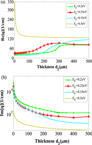
Figure 7. Dependences of TM GLSP propagation constant q versus buffer layer thickness for f = 0.3 THz, at different Fermi level values EF (a) real part, (b) imaginary part (logarithmic scale).
Download figure:
Standard image High-resolution imageOne can notice that for a thinner buffer layer, these modes become more damped and finally they are converted into short-range ones for small buffer thickness due to the stronger mode localization around the graphene layer. This effect is more pronounced for smaller Fermi level energies. GLSP for EF = 0.2 eV and EF = 0.25 eV are represented by short-range modes in the whole range of buffer thicknesses up to a very wide buffer thickness, when  for EF = 0.2 eV and
  for EF = 0.25 eV. GLSP modes are represented by long-range modes for
  when EF = 0.35 eV (
 for a very wide buffer thickness) and for
  when EF = 0.5 eV (
 for a very wide buffer thickness).
It is interesting to mention that GLSP dispersion dependences for EF = 0.35 eV and EF = 0.5 eV are markedly different (the same is valid for continuous MLSP branches shown in figure 5).
This is explained by mode modification spectrum analogously to that resulting in the MLSP splitting. The point is that dispersion dependences for GLSP mode and continuous MLSP branch become very close for Fermi level about EF = 0.48 eV and buffer layer thickness about 750 μm (see figure 8). This leads to a modified mode spectrum. As a result, the dependences for the real parts of the mode propagation constant values are repulsed in this region of buffer thickness for EF = 0.5 eV and GLSP mode (continuous MLSP branch) propagation constant dependence for EF = 0.5 eV turns out to be close to continuous MLSP branch (GLSP mode) propagation constant dependence for EF = 0.48 eV in the region of buffer thickness  .
.
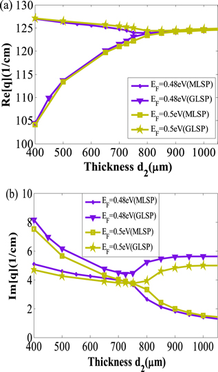
Figure 8. Dependences of the propagation constant q for continuous MLSP branch and GLSP versus buffer layer thickness for f = 0.3 THz at different Fermi level values EF (a) real part, (b) imaginary part.
Download figure:
Standard image High-resolution imageIf we replace GLSP dispersion dependence for EF = 0.5 eV in figure 7 by continuous MLSP branch dispersion dependences for EF = 0.5 eV taken from figure 5 we see that continuous MLSP branch dispersion dependences fits much better, the set of graphs plotted in figure 7 (the same is valid for the analogous replacement of graphs in figure 5). The modes are defined as graphene (metal)-like ones according to their behavior for very large buffer layer when d2 tends to infinity, therefore GLSP branches can be replaced by the MLSP ones due to the mode modification. At higher frequencies, one can show that the difference between propagation constant values of decoupled metal and graphene plasmons (see figure 2) becomes larger as the graphene surface conductivity  decreases due to the decreased intraband surface conductivity contribution
  (see equation (4b)).
Therefore, the graphene influence on the MLSP generally weakens and it is expected that modifications of the MLSP spectrum like that calculated for f = 0.3 THz (see figures 4 and 5) appear for a higher Fermi levels in graphene if the SP frequency is increased. Numerical calculations confirm this statement.
The behavior of MLSP for f = 0.6 THz is similar to that calculated for f = 0.3 THz, but the splitting of the MLSP takes now place for a larger Fermi energy EF = 0.22 eV. The MLSP modes for this frequency are characterized by the larger damping of the modified spectrum and by smaller values of buffer thickness d2c at the cutoff conditions compared to the case when f = 0.3 THz. Further increase of the SP frequency leads to the disappearance of the splitting effect for MLSP e.g. for a SP frequency f > 0.75 THz, the MLSP propagation constant dependences are represented by continuous finite functions within the whole range of buffer thicknesses.
Dependences of MLSP propagation constant on Fermi level values are shown in figure 9 for f = 0.3 THz and different buffer thicknesses. One observes the propagation constant modulation is the strongest for buffer thickness d2 = 150 μm when the MLSP splits up into two branches for  Both real and imaginary parts of the MLSP propagation constant can be effectively modulated by changing the Fermi level in graphene; modulation of the imaginary part of the propagation constant, in particular, can lead to a large increase of the MLSP damping and to the SP propagation blockage.

Figure 9. Dependences of MLSP branch propagation constant q versus Fermi level EF for frequency f = 0.3 THz at d2 = 50 μm, d2 = 150 μm, and d2 = 250 μm (a) real part, (b) imaginary part.
Download figure:
Standard image High-resolution image
These observations are in agreement with what was found in figures 4 and 5 where the MLSP propagation constant was considerably modulated by changing the graphene electron concentration. This effect is especially strong near the regions when SP splits up into two branches.
4. Conclusions
The dispersion dependences of TM graphene-metal coupled SPs were analyzed versus the buffer layer thickness and Fermi level in graphene. Calculations were mainly performed for sub-THz frequencies.
It is shown that TM SPs are represented by metal-like and graphene-like branches depending on their behavior for very thick buffer layers. For frequencies smaller than 0.75 THz (for the concrete structure under study), the MLSP split up into two branches depending on the graphene electron concentration: one of the branches (continuous MLSP branch) exists in the whole range of the buffer thickness and being a short-range mode for small thicknesses, another one (cutoff MLSP branch) undergoes cutoff and exists only within a limited range of buffer thicknesses smaller than the cutoff thickness. It is found that cutoff MLSP branches are represented by Brewster-type modes at the cutoff thicknesses and cutoff MLSP branches are converted into unphysical growing modes for larger buffer thicknesses. The graphene-like plasmons are converted into short-range modes for small buffer thicknesses due to strong mode confinement around graphene.
It is demonstrated that propagation constant values of SP mode near cutoff can be effectively modulated by changing the graphene electron concentration in the vicinity of the modes cutoff thicknesses.
Acknowledgments
The authors acknowledge Vrije Universiteit Brussel (VUB) through the SRP-project M3D2, the COST action MP1204 TERA-MIR, and the Libyan Ministry of Higher Education for technical and financial support.