


Abstract
We study the transport behavior of anti-dot graphene both theoretically and experimentally, where the term 'anti-dot' denotes the graphene layer to be nanostructured with a periodic array of holes. It has been shown that the electronic band structure of the anti-dot graphene can be described by a 4 by 4 effective Hamiltonian (Pan J et al 2017 Phys. Rev. X. 7 031043) with a gap around the Dirac point, attendant with a 0 to π variation of the Berry phase as a function of energy, measured from the band edge. Based on the diagrammatic method analysis and experiments, we identify an energy-dependent metal-to-insulator transition (MIT) in this two-dimensional (2D) system at a critical Fermi energy ɛc, characterized by the divergence of the localization length in the Anderson localization phase to a de-localized metallic phase with diffusive transport. By measuring the conductance of square samples with varying dimension and at different Fermi energies, experiments were carried out to verify the theory predictions. While both theory and experiment indicate the existence of a 2D MIT with similar localization length divergence exponent, the values of the critical energy ɛc and that of the localization length do not show quantitative agreement. Given the robust agreement in the appearance of a 2D MIT, we attribute the lack of quantitative agreement to the shortcomings in the theoretical model. The difficulties in addressing such shortcomings are discussed.
Export citation and abstract BibTeX RIS

Original content from this work may be used under the terms of the Creative Commons Attribution 4.0 licence. Any further distribution of this work must maintain attribution to the author(s) and the title of the work, journal citation and DOI.
1. Introduction
In the traditional scaling theory [1–3] of Anderson localization (AL) [4, 5], wave-functions in 2D systems are localized even with arbitrarily weak disorders. This indicates that no metallic state can survive in a large enough 2D systems because there are always disorders in realistic materials. In contrast, for 3D systems only if the strength of disorder is strong enough so that the conductance of the system is lower than a critical value, denoted the mobility edge, would the electronic wave-functions be localized. The physical picture of AL is the coherent backscattering mechanism [3, 6–9], in which any multiply-scattered pathway and its time-reversed counterpart can interfere constructively, leading to enhanced backscattering. In 2D, this mechanism gives rise to a cumulative downward renormalization of the diffusion coefficient to zero, even with arbitrarily weak disorders, thereby leading to AL.
Recently, new 2D material systems, e.g. graphene-based materials [10–12] and symmetry-protected surface states of topological materials [13–22], structure symmetry is shown to introduce an additional geometric phase factor, denoted the Berry phase, that suppresses the back-scatterings and results in the anti-localization effect [23–38]. Transport in such 2D system can be super-diffusive [31, 39–42], indicating the existence of the 2D metallic phase.
Anti-dot graphene is a single graphene layer nanostructured with a periodic array of holes; this leads to the opening of a gap around the Dirac point [43–45], and the introduction of a variable Berry phase, changing from 0 close to the band edge, to π far away [43]. As a result, one can expect the traditional coherent backscattering behavior to be dominant close to the band edge, and anti-localization behavior would dominate at energies far away. Hence such a Berry phase variation can potentially induce a MIT. In fact, localization to anti-localization transition in topological materials has been addressed previously [18, 21, 22], but they were focused on the behavior of magneto-resistance, rather than on the large-scale transport properties. Furthermore, the Hamiltonian of anti-dot graphene is different from that of topological insulators. To our knowledge, large-scale transport properties associated with the Berry phase variation in anti-dot graphene systems have not yet been studied.
In this work, we investigate the problem of two dimensional (2D) metal–insulator transition in anti-dot graphene both theoretically and experimentally. The manuscript is organized as follows. In section 2 we present the results of a diagrammatical theory to analyze the multiple scatterings in anti-dot graphene; we describe the main results in the main text—the 2D localization to anti-localization transition at a critical Fermi energy ɛc above the band edge. The supporting theoretical derivations are described in the supplemental materials. In section 3 we describe the experiment that led to the observation of the diverging behavior of the localization length at a critical Fermi energy level ɛc, and diffusive transport behavior above ɛc. In section 4 we compare the theoretical prediction and the experimental results. While the MIT is observed both theoretically and experimentally, the value of the ɛc and the localization length are not in quantitative agreement; the latter is attributed to a crucial shortcoming of the theoretical model. We recapitulate our results in section 5.
2. Theoretical analysis of large-scale transport of anti-dot graphene
Consider an anti-dot graphene decorated by a disordered scalar potential. A scanning electron microscopy (SEM) image of the anti-dot graphene sample is shown in figure 1(a). A schematic illustration of the holes array on graphene is shown in figure 1(b). The periodic hole structure introduces a new Bravais lattice into the graphene layer, leading to the opening of a gap at the Dirac point. An effective anti-dot graphene Hamiltonian is [43]:

with quasiparticles being described by the four-component Bloch functions: ![$\psi ={\left[\begin{matrix}\hfill {\phi }_{{\boldsymbol{K}}_{+}A}\hfill & \hfill {\phi }_{{\boldsymbol{K}}_{+}B}\hfill & \hfill {\phi }_{{\boldsymbol{K}}_{-}B}\hfill & \hfill {\phi }_{{\boldsymbol{K}}_{-}A}\hfill \end{matrix}\right]}^{\mathrm{T}}$](https://content.cld.iop.org/journals/1367-2630/24/11/113027/revision2/njpac9f2aieqn1.gif) . Here we denote the two 'valleys' by
K
+/
K
−, and the two inequivalent carbon 'sub-lattices' by A/B, illustrated in figure 1(c). Electronic momentum
p
=
k
−
K
+(
K
−) is measured from the Dirac points,
. Here we denote the two 'valleys' by
K
+/
K
−, and the two inequivalent carbon 'sub-lattices' by A/B, illustrated in figure 1(c). Electronic momentum
p
=
k
−
K
+(
K
−) is measured from the Dirac points, 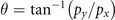 denotes the angle of the propagation, and υ denotes the group velocity of electrons in antidot graphene. Here m is the mass term, arising from the scatterings by the periodic hole array, that leads to a gap of 2m around the Dirac point. In this work we employ the system of atomic units by setting the Plank constant and the electronic charge to be unity, i.e. ℏ = e = 1. H0 gives rise to a massive energy spectrum
  , in contrast to ɛ = ±υF
p for pristine graphene, where υF denotes the Fermi velocity.
, in contrast to ɛ = ±υF
p for pristine graphene, where υF denotes the Fermi velocity.

Figure 1. (a) A SEM image of an anti-dot graphene sample. The anti-dot array is a hole array nanostructured on a monolayer graphene sample, with a periodicity ∼150 nm and a pore diameter ∼100 nm. (b) An illustrative plot for the holes on the graphene. Red circle delineates the boundary of a hole. Electrons are scattered from the boundary, thereby inducing a new periodicity in the system. (c) Lattice structure of a graphene monolayer. Carbon atoms are arranged in a hexagonal lattice, and white/black atoms represent the A/B sub-lattices, respectively. (d) The anti-dot boundary scatters electrons and induces a gap around the CNP. The scale to the right indicates the variation of the Berry phase in unit of π.
Download figure:
Standard image High-resolution imageIn the conduction band, the Berry phase around the Dirac point, given by  , is energy-dependent and varies from 0 at the band edge (ɛ = m) to ∼π at high energies ɛ ≫ m. Such a variation is illustrated in figure 1(d). This implies the potential existence of a localized phase around the band edge and an anti-localized phase at high energy. As a consequence, this fact strongly indicates that at some critical energy ɛc the transport characteristic can undergo a phase transition between these two phases.
In order to study the large-scale electronic transport in anti-dot graphene, we derived a density response theory to describe the transport in anti-dot graphene. Here we present the main results. Detailed derivations are summarized in the supplemental materials [46] for interested readers. We identified a metal–insulator transition with ɛc being the solution of the transcendental equation of ɛ:


Here  , and τ0 is the elastic scattering time of the disorder potential. When the Fermi energy is below ɛc the system is localized; metallic, diffusive transport behavior is found above ɛc. The correction to the diffusion coefficient, δD, is a function of both energy and system size scale L, given by the relation:

Here D0 = υ2 τ and l is the mean free path. There is a second critical energy ɛc2 > ɛc that distinguishes the weak-localization region and the anti-localization region, by setting the right-hand side of equation (3) to zero. If the Fermi energy is in the insulating region m < ɛ < ɛc, the diffusion coefficient D decreases to zero as system size scale L increases to infinity. In the weak-localization region ɛc < ɛ < ɛc2, the diffusion coefficient D decreases and reaches at some non-zero plateau value that is smaller than D0 as L increases to infinity. In the anti-localization region ɛc2 < ɛ, D increases with increasing L and reaches a saturation value that is larger than D0. This behavior is shown in figure 2.
Figure 2. The renormalized diffusion coefficient plotted as function of the system size L/l, where l is the mean free path. Below the critical energy εc the diffusion coefficient can be renormalized to zero, indicating localization. Between εc and εc2, the coherent backscattering can downward modify the diffusion coefficient (note the slightly downward trend of the red curve at small system size), but approaches to a plateau value smaller than D0. Above εc2, the renormalized diffusion coefficient increases to a saturation value that is larger than D0. These behaviors indicate a localization to anti-localization transition. In this case εc ∼ 20 meV and εc2 ∼ 30 meV.
Download figure:
Standard image High-resolution imageCompared to the pristine graphene [33], there are two important differences—(1) the appearance of the localization/weak-localization phase, and (2) the saturation of the diffusion constant D as L increases to infinity.
From the theory, we can also obtain the localization length ξ in the localized region, defined as the length scale at which the diffusion coefficient decreases to zero:

ξ diverges as the energy approaches the critical energy ɛc from below. The critical exponent characterizing the divergence of the localization length,  , is η ∼ −0.5.
3. Experimental study of large-scale transport of anti-dot graphene
To verify the existence of the suggested localization to de-localization transition, we carried out transport measurements on the anti-dot graphene samples. We employed e-beam lithography and oxygen plasma etching to pattern the anti-dot structures on monolayer graphene, with a period ∼150 nm and anti-dot diameter ∼100 nm (see figure 1). Multiple contacts were defined in a second e-beam lithography step, and then 10 nm Ti and 80 nm Au were deposited by e-beam evaporation. A uniform background gate was employed to modulate the Fermi energy in the system. An illustrated picture of the system is shown in figure 1. The localization length ξ was extracted at 2 K by following the same method as introduced by reference [47], i.e. by varying the size of the square samples.
We have fabricated the anti-dot graphene sample in the Hall bar geometry with varying spacing between the electrodes in the longitudinal direction. The sample lengths vary from 2.5 to 11.5 μm, as presented in the SEM picture in figure 3(a). The gate voltage dependence of conductivity is plotted in figure 3(b). At each fixed gate voltage, we measured the conductance g as a function of sample size scale L, and the localization length was extracted using the expression:

to fit the conductance data. The energy shift was obtained based on the massive energy dispersion  , where ℏ is the reduced Planck constant,
  is the Fermi wavevector, n = 7.57 × 10¹⁰ × VG /cm2⋅V is the carrier density that can be extracted from the geometric capacitance of the global back gate, and m is the mass term that we discussed before.

Figure 3. (a) SEM image of the measured device. (b) VG dependence of the conductivity corresponding to L = 2.5 μm sample length. The shaded regime corresponds to the energy scale discussed in the main text. (c) Conductivity measured as a function of sample length L at varying energy shift. It is clear that if ε − εCNP < 33 meV the system is localized, and at ε − εCNP = 43 meV the system is diffusive. There is a localization-to-diffusive transition that occurs between these two doping levels.
Download figure:
Standard image High-resolution imageIt can be seen from figure 3(c) that a localization to de-localization transition occurs when the energy shifts away from the charge neutrality point (CNP). At around the CNP, the conductance follows the scaling theory (equation (5)), indicating the system lies in the localization regime. As the energy shifts away from the CNP, the system was observed to shift abruptly to the diffusive regime—that is, the square conductance becomes a constant when ε − εCNP > 43 meV.
4. Comparison between theory and experiment
We now show the comparison between theory and experiment. The theory prediction of the localization length vs energy shifting— in the localization regime, with ɛc ∼ 20 meV and then diverges to infinity in the de-localization regime—is plotted in figure 4(a). The experimentally measured localization length ξ versus energy shifting is shown in figure 4(b). As the energy shifts away from the CNP, the localization length is observed to grow dramatically and finally diverges at a certain critical energy ɛc, which is exactly the same behavior predicted by the theory as shown in figure 4(a). Based on the theoretical prediction, i.e.
  , we perform a fitting to the experimental data to determine the critical energy ɛc and the divergence power exponent η, respectively. The fitting result is plotted in figure 4(b) by the red line, which yields ɛc ∼ 33.5 meV and η ∼ −0.44. The divergence power exponent η ∼ −0.44 matches reasonably well with the theoretically predicted divergence exponent of −0.5. Therefore, the theoretical analysis is in qualitative accords with the experimental results. Both theoretically and experimentally, the prediction of a 2D localization to de-localization transition is verified. As described in the last section, the localization to de-localization transition arises from the negative to the positive transition of the conductance correction. Physically, this sign change is the result of the Berry phase variation, representing the constructive to destructive interference in the back-scattering. Hence the localization to de-localization transition originates from the variable Berry phase as a function of the Fermi energy. However, from the experimental data we cannot deduce the value of
  .
.

Figure 4. (a) The theoretical data of the localization length ξ versus Fermi energy. The mean free path is ∼30 nm and m ∼ 10 meV which is extracted from the experimental data. (b) The experimental result of the localization length ξ versus Fermi energy. The red line is a fit to the experimental data which gives a critical energy ɛc = 33.5 meV and η = −0.44. Both the experimental data and the theoretical result indicate that the localization length ξ diverge at some critical energy εc, which verifies the localization–delocalization transition. The mismatch between the experimental data and the theoretical result can be attributed to three points, the states inside the gap that are not considered in the model, the one-loop calculation method, and the puddles in realistic anti-dot graphene systems, as discussed in the main text.
Download figure:
Standard image High-resolution image
Quantitatively, we can estimate the critical energy with the corresponding data of the experimental case. According to the tight-binding model of anti-dot graphene [43], the mass term m is ∼10 meV in our experiments. Substituting this value into the theory, the estimated localization length as a function of Fermi energy is shown in figure 4(b). In the plot, we have assumed that the mean free path l = υτ = 30 nm to match the experimental observation. The obtained critical energy is ∼20 meV, about ∼10 meV higher than the band edge. As a comparison, in the experiments, we observed the critical energy is ∼35 meV. Hence the theoretical result is somewhat smaller than the experimental observations. However, the estimated localization length from our theoretical model is much smaller than what is observed in the experiments. This discrepancy can be attributed to three possible reasons, discussed below.
The low-energy effective Hamiltonian equation (1) is extracted from the tight-binding calculation [43] and is valid only in the conduction/valence band. Around the CNP there are extra complexities that are not taken into account. According to the recent work [48], there can be localized states with a constant DOS in the anti-dot gap. These effects are taken into account with the tight-binding calculation but cannot be included in the effective Hamiltonian, equation (1). As a result, around the CNP, the correlation effect introduces a much smaller 'hard gap' in the DOS of localized states and suppresses the inelastic scattering processes. The phase coherence between the states around CNP can be preserved up to an extremely long length/time scale. The tight-binding model also predicts these states around CNP show power-law decay behavior away from the hole-edge. Therefore, AL may have emerged from such states. If so, then the AL behavior observed in the experiment may be partially attributed to these states that are inside the anti-dot structural gap, which is not taken into account in the present theoretical model. This can be the main source of the theory-experiment disagreement.
There are some other potential sources for the theory-experiment disagreement. The anti-dot graphene sample is placed on silicon dioxide substrates, which is well known to induce electron–hole puddles [11]. Consequently, local potential fluctuations can be relatively long-range, which may affect the localization region in the energy spectrum, as well as the localization length. Also, the theoretical analysis is perturbative. It only takes into account the 'one-loop' [39, 42] diagrams. The perturbative treatment is accurate only if  is satisfied. However, in the localization region, the correction to conductance is comparable or even larger than D0. As a result, we do not expect that our one-loop perturbative calculation can describe the whole problem very accurately.
The difficulty in including the gap states in the theoretical model lies in the lack of an accurate boundary condition, besides the normal current =0 at the hole edge, so that the continuum model can reproduce the tight-binding results, in particular the gap states. This difficulty is currently being addressed.
The results found in this research can actually be of practical use. This is because if there is a localized (insulator) and delocalized (metal) transition at a critical doping level, which means one can manipulate the conductance at the mesoscopic level by just varying the gating voltage. Since the electrical signals can be extremely fast, hence locally, the control on the conductance can open and shut current flows, to simulate input signals.
5. Conclusion
To conclude, we validate both theoretically and experimentally the existence of a 2D localization–delocalization transition in anti-dot graphene systems. The coherent backscattering process gives rise to a varying Berry phase, leading to a negative conductance correction close to the band edge, and a positive correction at a higher doping level. The localization length diverges at a critical Fermi energy, which is verified both theoretically and experimentally with a similar divergence exponent. However, the predicted localization length is order of magnitude smaller than that observed experimentally. We discuss the potential sources of quantitative theory/experiment disagreement that can remedy the situation if corrected.
Acknowledgments
The data that support the findings of this study are available upon reasonable request from the authors.
Data availability statement
No new data were created or analysed in this study.