


Abstract
Multiferroic materials that exhibit coupling between ferroelectric and magnetic properties are of considerable utility for technological applications and are also interesting from a fundamental standpoint. When reduced to the nanoscale, multiferroic materials often display additional functionality that is dominated by interfacial and confinement effects. Bismuth ferrite (BiFeO3) is one such material with room temperature anti-ferromagnetic and ferroelectric ordering. Optical excitation of BiFeO3 crystals results in an elastic structural deformation of the lattice with a fast response on the pico-second time scale. Here we report on dynamic measurements to investigate the structural properties of BiFeO3 nanoscale crystals using laser excitation and three-dimensional Bragg coherent x-ray diffraction imaging. Tensile strain beyond 8  was observed predominantly at the surface of the nanoscale crystal as evidenced in the reconstructed phase information and was correlated to photo-induced lattice deformation.
Export citation and abstract BibTeX RIS

Original content from this work may be used under the terms of the Creative Commons Attribution 3.0 licence. Any further distribution of this work must maintain attribution to the author(s) and the title of the work, journal citation and DOI.
1. Introduction
Single phase materials that simultaneously exhibit more than one ferroic property including ferromagnetism, ferroelectricity, ferroelasticity or ferrotoroidicity are often described as multiferroic [1–3]. Many of these materials are transition metal oxides with perovskite crystal structure. They are of great interest as the interplay between multiple ferroic properties has numerous potential applications [4–7]. For example, the coupling between magnetic and ferroelectric ordering can be utilised to develop magnetoelectronic devices where spin transport can be controlled electrically. As a result there is a vibrant effort to understand the underlying mechanisms at play in bulk and thin film materials. To date however there are fewer studies dedicated to understanding multiferroics in the nanoscale setting. This is largely due the the limited tools that are able to probe crystalline and magnetic structure on the nanoscale. Moreover, when multiferroic materials are scaled down to the nanoscale, their functional properties are increasingly dominated by surface effects. As a result, conventional means to describe their behaviour must account for surface and interfacial properties.
Bismuth ferrite (BiFeO3) is a perovskite metal-oxide semiconducting material with a band-gap of 2.8 eV that shows both antiferromagnetic and ferroelectric ordering at room temperature. When compared with the conventional bulk perovskite structure, BiFeO3 can be described as rhombohedrally distorted with lattice constants of a = 5.63 Å and  . The rhombohedral unit cell consists of two conventional perovskite unit cells with the two oxygen octahedra rotated by
  about the [111] plane. In addition, the Fe atom is shifted away from the octahedral centre while the Bi atom is shifted away from the conventional position between the octahedral centres [8–10]. Ferroelectric ordering in BiFeO3 therefore results from the reduction in symmetry due to the two Fe–O bond lengths. In BiFeO3 each Fe ion is surrounded by six neighbouring Fe ions with antiparallel spin orientation leading to G-type antiferromagnetic ordering and a coupled long-range incommensurate spin-cycloid antiferromagnetic ordering along the [110] direction with cycle length of 62 nm. Magnetic ordering results from the spontaneous breaking of time reversal symmetry while and ferroelectric ordering is due to spatial inversion symmetry breaking and is permitted as a result of the lack of inversion symmetry in the lattice, of space group R3c. Coexistence of the two phenomena is generally observed in perovskite structures where the ferroelectric displacement from centrosymmetry occurs in the non-magnetic ion. In the case of BiFeO3, the ferroelectric displacement is primarily due to a distortion of the Bi ions from a centrosymmetry configuration. BiFeO3 also exhibits a significant visible light-mediated photostrictive effect with magnitude dependent on the intensity and polarisation of the light field. It has promising applications in magnetoelectric memory storage and electric-field control of magnetic sensors and photovoltaics [4, 5, 11]. Here we are interested in studying the visible light photostrictive effect using coherent x-ray diffraction imaging (CXDI). Using this technique, we are able to observe a three-dimensional structural deformation of the lattice that correlates with increasing continuous wave visible laser light illumination. Our observations suggest that structural distortion results from photoexcited charge carriers that are separated by the ferroelectric polarisation field within the crystal.
CXDI is a lens-less far field imaging technique that allows imaging of nanometre scale crystalline materials with a sensitivity below a single angstrom. Due to the high penetration power of x-rays in matter, CXDI is largely non-destructive and provides information on how atoms are displaced from a reference position at the surface and throughout the bulk of a material [12]. Bragg CXDI is performed by illuminating a sample with a spatially coherent x-ray source so that the coherence length exceeds the dimensions of the crystal, in the Bragg reflection geometry. Coherent light scattered from the entire volume of the crystal will interfere and produce a three-dimensional speckle pattern in the Fraunhofer limit [13]. Two-dimensional slices of the diffracted intensity are measured using an area detector which is positioned far enough away from the sample to resolve the finest fringes of the speckle pattern. The third-dimension is obtained by rotating the Ewald sphere through the Bragg condition while maintaining a largely fixed incident and reflected wave vector (the rocking curve technique). When performing CXDI measurements, only the intensity of the speckle pattern  is recorded and the phase information (ϕ) is lost. Provided that the crystal has sufficiently few defects and is well-faceted, a speckle pattern is observed with sufficient fringe visibility to permit inversion and recovery of the phase information. If the speckle pattern is sufficiently oversampled, inversion is possible to recover the complex three-dimensional electron density of the object and its phase information by using iterative projection phase retrieval techniques. We are then able to directly relate the recovered phase information to the atomic displacements in the direction of the wave transfer vector
  as
as  , where
  is the average unit cell displacement vector [14–17]. Algorithmically, phase information is recovered by propagating the corresponding electron density
  of the measured intensity back and forth between the sample and detector planes. This is equivalent to a transformation between direct and reciprocal space, respectively. At each turn a constraint is imposed according to the physical properties of the imaging field [18–21]. In reciprocal space, the computed modulus of the object propagated to the detector plane,
  , must almost everywhere reside in the set of points with amplitude
  . In direct space, the density of the object is non-zero within a confined 'support' region and is minimised in some way outside of this region. When both constrains are simultaneously satisfied a solution is found.
2. Experiment
Single crystals of BiFeO3 are readily synthesised by solid phase reaction between Bi2O3 and Fe2O3 powders. This process however is plagued by the presence of parasitic intermediate phases that tend to seed and grow from grain boundary sites [22–24]. To obtain high quality material, BiFeO3 nanoscale crystals were synthesised on r-plane sapphire substrates using a pulsed laser deposition (PLD) technique. A solid target of BiFeO3 was used as source material and ablated using a 248 nm, 20 mJ KrF excimer laser system in an oxygen partial pressure of 0.03 hPa. X-ray diffraction measurements confirmed single phase BiFeO3 growth constituents when PLD synthesis was performed at 550 °C. Nanocrystal sizes were largely dependent on the duration of the synthesis process and the laser fluence. Synthesising for 30 min with a repetition rate of 200 Hz was sufficient to yield highly faceted nanocrystals of BiFeO3 approximately 200 nm in size (figure 1(b)).
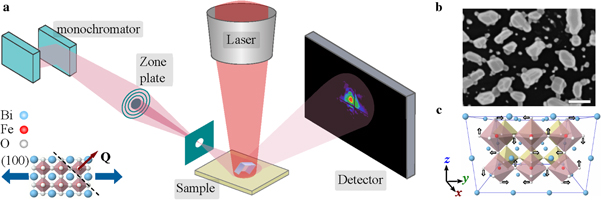
Figure 1. (a) Experimental geometry at the coherence branch of beamline I13, diamond light source. (b) Electron micrograph of BiFeO3 nanocrystals as synthesised on r-plane sapphire (1 μm scale bar is shown). (c) Illustration of oxygen octahedral tilting in the ideal perovskite structure that results in the rhombohedrally distorted BiFeO3 structure. Inset of (a) depicts the BiFeO3 lattice structure and the wave transfer vector normal to the (110) lattice plane. The photo-induced structural deformation is directed normal to the (100) lattice plane.
Download figure:
Standard image High-resolution imageExperiments were performed in air at the coherence branch of beamline I13 at the diamond light source [25]. A double bounce Si (111) monochromator was used to select an energy of 9.1 keV corresponding to the minimum gap (6.15 mm) of the U25 (2.8 m) undulator insertion device (ID) in 'mini-beta' configuration. The horizontal spatial coherence was directly tuned by closing white-beam slits located at the virtual focus of the ID. The beam was condensed to 10 μm using a defocussed, blazed, zoneplate assembly (D = 400 μm,  , efficiency 35%). To reduce vibrational effects, but allow the long propagation distances required for Bragg CXDI experiments, the 3 mega-pixel photon counting Excalibur detector [26] along with the 2 m flight-tube was mounted using a robotic cell comprising two industrial robots controllable through EPICS, mechanically separated from the sample goniometer. A polarised 632.8 nm Helium–Neon (HeNe) laser was focussed via a 0.28 NA microscope objective on to the eucentric point of the sample goniometer and aligned to the x-ray beam. A sample of sparsely arranged BiFeO3 nanocrystals was mounted onto the goniometer assembly, a single nanocrystal aligned to the eucentric point and the (110) specular reflection located. The crystal was then irradiated with the HeNe radiation of variable intensity by attenuation through a combination of 8 N-BK7 reflective neutral density (ND) filters with transmissions ranging from 1% to 79%. The power was then modulated up to a maximum of 20 mW by selectively removing ND filters.
Experimental results were gathered by identifying the speckle pattern of a single nanoscale crystal of BiFeO3 on the area detector and then acquiring the three-dimensional speckle pattern using the rocking curve technique. The crystal was then illuminated with successively more intense red laser light by removing a single ND filter from the path of the beam. At each interval, the resulting speckle pattern was acquired. Amplitude and phase reconstruction of the object from the speckle pattern was carried out using a custom version of the 'shrink-wrap' algorithm found in the interactive phase retrieval suite [27]. This was found to improve convergence of the algorithm by defining a support region with a morphology that mimics that of the reconstructed object. For each speckle pattern, 103 iterations of the hybrid input–output (HIO) algorithm were performed first using a loose support to allow an unrestricted solution to form. A total of  iterations of the HIO algorithm were performed with the support updated at intervals of 500 iterations. Subsequently, 103 iterations were performed of the phase-only HIO algorithm that optimised the phase while leaving the amplitude unchanged.
3. Results and discussions
Line scans of speckle patterns taken from the (110) reflection of a single BiFeO3 nanocrystal are shown in figures 2(c) and (d). This is accompanied by two-dimensional slices of the speckle patterns (2(a) and (b)) to indicate the direction of each set of line scans. A progressively distorted speckle pattern is observed. As the photo-induced structural deformation effect is directed normal to the (100) lattice plane, a component of the deformation is directed along the wave transfer vector  . This is significant as it allows us to quantify the component of atomic displacement along this direction from the phase of the reconstructed object. Photo-induced structural deformation will therefore result in an atomic displacement field
  with structure that is determined by the ferroelctric and magnetoelectric response. The resulting instantaneous scattering amplitude is given by [17]:

In each line scan shown in figures 2(c) and (d) the wave transfer vector is fixed while the illumination intensity of the laser is exponentially increased from zero to 2.5 W cm−2. Upon increasing the excitation laser intensity, distortions in the speckle pattern began to appear and were manifest as increased asymmetry in the speckle pattern resulting largely from localised changes in the intensity distribution. This asymmetry was previously associated with lattice strain in the material. It is possible to quantify changes in each speckle pattern by contrasting the intensity sum of the cross-correlation for each successive speckle pattern with that of the unperturbed speckle pattern. If the cross-correlation of the nth successive speckle pattern  with that of the unperturbed is denoted as
  , then the normalised change in sum
  is given by:

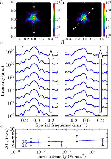
Figure 2. Two-dimensional slices of the speckle pattern of a single BiFeO3 nanocrystal unilluminated (a) and illuminated with maximum intensity of 2.5 W cm−2 of 632.8 nm wavelength laser light (b). Line scans along the path indicated in each speckle pattern for increasing intensity are shown in (c) and (d), respectively. The arrow indicates the direction of increasing illumination intensity. The change in intensity of the cross-correlation measure for each speckle pattern is shown in (e).
Download figure:
Standard image High-resolution imageHere,  is the auto-correlation for the unperturbed speckle pattern. This result is shown in figure 2(e) along with a linear fit to the change in correlation sum with the logarithm of the laser intensity. Deformation of the speckle pattern therefore rapidly increases with an increase in the intensity of the excitation source and then saturates as laser intensity approaches 1 W cm−2. This effect was found to persist in all samples measured. The inset of figure 4 demonstrates repeatability of this effect when the laser illumination is repeatedly cycled between off and on states.
The reconstructed amplitude and phase of the BiFeO3 nanocrystal is shown in figure 3. Reconstruction is shown in the absence of laser illumination ((a), (b), (c) and (d)) and with maximum laser illumination of 2.5 W cm−2 ((e), (f), (g) and (h)) to correspond with speckle patterns in figures 2(c) and (d). An isosurface of 86% is used in each rendering of the objects amplitude. The nanocrystal was found to have nominal dimensions of 300 × 280 × 150 nm and was reconstructed with a resolution down to 15 nm. Morphological features associated with the rhombohedral crystal structure can be seen in the reconstruction along with finer step-terraced surface features along the Cartesian z-axis direction, as indicated in 3(f). The experimental wave transfer vector direction is also indicated in figure 3 and appears normal to the x–y plane. Phase information mapped onto the isosurface of the object is shown in figures 3(c), (d), (g) and (h). Without laser illumination ((c) and (d)), the phase information at the surface contains regions of positive and negative phase indicating the presence of tensile and compressive strain near to the surface. The phase approaches zero towards the centre of the nanocrystal with only a small and compact region of negative phase down to −0.39 radians remaining at its centre. This is more easily observed in the phase line scans shown in figure 4. Although BiFeO3 is known to form ferroelectric domains, no phase wraps in the phase information, that might be associated with domains boundaries, were observed in our samples [28–30].
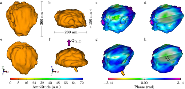
Figure 3. Reconstructed amplitudes and phases for a single BiFeO3 nanocrystal in the absence of laser illumination ((a), (b), (c) and (d)) and with maximum laser illumination ((e), (f), (g) and (h)). All amplitudes are shown at an 86% isosurface. Phase information is mapped onto the surface of the object in (c), (d), (g) and (h). In addition, (d) and (h) show the reconstructed amplitudes with a quadrant section removed to reveal phase information through the bulk of the nanocrystal.
Download figure:
Standard image High-resolution image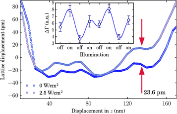
Figure 4. Line scans of the reconstructed phase through the centre and along the orthogonal z-direction (figure 3) of the BiFeO3 nanocrystal, in the absence of and during laser illumination with 2.5 W cm−2 of 632.8 nm wavelength laser light. The inset shows variation in  when the laser illumination is repeatedly cycled between off and on states (The line is a fit to the data and serves only as a guide).
Download figure:
Standard image High-resolution image
For the case of maximum illumination (figures 3(g) and (h)), the phase towards the surface is now prominently positive in value suggesting an overall increase in tensile strain. The observed increase in phase (as indicated in figure 3(g)) is equivalent to a lattice displacement of upto 23.6 ± 2 pm and an induced inter-planar strain of upto  at the surface of the nanocrystal. Phase information within the bulk of the nanocrystal is redistributed with a reduction in size of the region of narrowly varying negative phase at the centre of the nanocrystal and broadening of the surrounding region of zero phase in its immediate vicinity. This effect is indicated in figure 3(h). A trivial phase shift in the solution as permitted by Fourier amplitude measurements (as
  ) cannot account for this effect as broadening of regions where the phase varies narrowly is observed, as opposed to a uniform shift in phase (see also figure S1 of the supplementary material). Instead it is likely due to deformation of the lattice as a result of light-mediated photostriction. This effect is thought to result from photo excited electron–hole pairs created by the photovoltaic effect within the material that are subsequently separated by the electric field due to the internal polarisation. Their separation yields an internal voltage that further induces a reverse piezoelectric effect. This is further supported by the rapid saturation of
  as shown in figure 2(e).
As bulk single crystal BiFeO3 is known to have fewer defects than thin films and generally exhibits a low leakage current and a spontaneous electric polarisation that is comparable to the theoretical value of 90 μC cm−2, we can expect self-assembled BiFeO3 nanocrystals to also have a comparatively low density of crystalline defects when compared to thin films [31–33]. In addition, Bragg CXDI has angstrom sensitivity to crystalline defects and is not suited to the study of amorphous or polycrystalline materials. This suggests that any defects present in BiFeO3 nanocrystals used here are of a sufficiently low concentration to permit Bragg CXDI measurements. High electrical leakage currents that result from defects such as oxygen vacancies are therefore less likely to occur in self-assembled BiFeO3 nanocrystals for this same reason. This reasoning is also supported by the absence of tensile strain in the bulk region of the nanocrystal that might be associated with free charges that persist in the absence of laser illumination (figure 4).
While the photostrictive effect was understood to occur in previous studies where band-edge illumination was used as an excitation source, it is also known to occur with below band-gap excitation[11, 34]. This can be understood if the photostrictive effect in BiFeO3 is considered to include a magneto-electric coupling component that additionally couples to Fe3+ ions in the lattice. Similar findings were made in neutron scattering experiments [35–38]. The observation of a surface dominated photostrictive effect was not anticipated as the absorption length in our experiments exceeds the dimensions of the nanocrystal [39, 40]. This suggest a need to consider additional surface effects for an adequate description of light-mediated photostriction in BiFeO3 nanocrystals.
4. Conclusion
The possibility of harnessing multiferroic compounds such as BiFeO3 that can operate at room temperature is desirable for the realisation of numerous technological applications. We have shown that photostriction in BiFeO3 is both stable and repeatable in nanoscale crystals and results in tensile strain in the lattice structure upon illumination. We have also demonstrated the use of Bragg CXDI for observing lattice distortions in dynamical studies. This approach can be extended for the study of ultra-fast processes in BiFeO3 nanoscale materials using sub pico-second laser excitation and femto-second hard x-rays available at free-electron laser facilities.
Acknowledgments
This work was supported by the Royal Society Research Grant RG/130498 and a Japan Society for the Promotion of Science (JSPS) Kakenhi grant 24681014. The Diamond Light Source is kindly acknowledged for the provision of beam time.