
Abstract
Confinement in small structures has required quantum mechanics, which has been known for a great many years. This leads to quantum transport. The field-effect transistor has had no need to be described by quantum transport over most of the century for which it has existed. But, this has changed in the past few decades, as modern versions tend to be absolutely controlled by quantum confinement and the resulting modifications to the normal classical descriptions. In addition, correlation and confinement lead to a need for describing the transport by quantum methods as well. In this review, we describe the quantum effects and the methods of treament through various approaches to quantum transport.
Export citation and abstract BibTeX RIS

Original content from this work may be used under the terms of the Creative Commons Attribution 4.0 license. Any further distribution of this work must maintain attribution to the author(s) and the title of the work, journal citation and DOI.
1. Introduction
A knowledgeable reader might be tempted to ask the question, 'hasn't all transport in semiconductors devices been quantum mechanical?' The answer, of course, is 'yes', but it is a qualified yes, as there are several levels in which quantum mechanics may be involved, especially if we consider that almost one century has passed since the concept of the field-effect transistor (FET) was first discussed. Indeed, theories of quantum mechanics were just being proposed, so Lilienfeld's ideas were, by necessity, entirely classical [1] 4 . Yet, the wave nature of the electron, and the periodicity of the crystal lattice, are the base upon which the idea of the band structure is based. Nevertheless, the introduction of an effective mass for the quasi-particles (the electrons and holes) freed the scientist from worrying about such things, and allowed one to proceed as if the carriers were classical objects.
This view was reinforced by Kennard [2], who began with the Schrödinger equation and developed a hydrodynamic corollary, and then observed that the electrons would move just as classical particles would respond to the fields and potentials, but that there would be an additional quantum force/potential. It is this quantum potential that is folded into the concept of effective mass. Then, of course, the scattering of carriers by the quantized vibrations of the lattice, the phonons, is treated quantum mechanically, but only to the extent necessary to describe a probability for scattering that is used in classical transport equations. Finally, it is the third level of quantum effects, such as confinement in small structures, for which quantum mechanics needs to re-enter the picture, and it is here that one has need to deal with quantum transport. As a result, the FET has had no need to be described by quantum transport over most of the century for which it has existed. But, this has changed in the past few decades, as modern versions tend to be absolutely controlled by quantum confinement and the resulting modifications to the normal classical descriptions. One need look no further than the introduction of strain into the channel of the FET, which is done to modify the effective mass and electronic structure, to recognize this [3].
But, having said this, if one were to conduct a poll of say 100 experienced device engineers, there would be no overall demand for a study of quantum transport, as most see no need for this level of sophistication. To counter this, we need only point out that for a long part of the history of FETs, these same engineers saw no need for any modeling or simulation. Of course, this is no longer the case, and it may be expected that the need for quantum transport will become more important in the near future. And perhaps, with this review, a number of the quantum effects that may be surprising, will appear to the readers to change their minds. Recognizing these points, it is the 3rd level of quantum mechanics and transport mentioned above that will be discussed in this review. In the following sections of this introduction, a brief history of the FET, its scaling, requirements, and modeling will be introduced. This will be followed by a discussion of just what kind of quantum effects occur and how they affect the transport. A discussion of how quantum transport differs from classical transport will be presented, followed by a discussion in the next sections.
1.1. Evolution of the FET
While the Lilienfeld patent is generally considered to be the start of the FET, it is not all that clear from the description in the patent, and it was a later patent by Heil that more clearly described the surface-oriented device [4]. It is generally believed that the work at Bell Telephone Laboratories was attempting to make the device in Ge, but the lack of a stable oxide led them to the point contact transistor (two metallic points attached to the Ge layer) [5], developed by Bardeen and Brattain [6, 7]. Shockley would shortly follow this with the junction transistor (diffused or grown layers of various doping) [8].
Bringing the FET to reality would take somewhat longer. Atalla stabilized the Si surface with a thermal oxide [9], and this led he and Kahng to develop a MOSFET around 1960. Atalla got irritated at Bell's disinterest in the MOS technology and left in 1962; perhaps this is the reason why Kahng is the sole author of the patent [10]. Fortuitously, others in California recognized the advantages of MOS technology that eventually led to its use in integrated circuits through two patents filed in 1959 [11, 12].
Complementary n-channel and p-channel devices appeared in 1962 [13, 14], as low power devices which eventually dominated the continued development of integrated circuits and became the well-known CMOS. The advantage possessed by these devices lay in their planar layout (the plane of the current flow is in the layer plane, whereas it was normal to the plane in a junction bipolar transistor), which was much favored for large scale integration, and their low power dissipation. Growth in the technology is largely measured by Moore's law; the idea that the dimensions would decrease from one generation to the next with the result that the number of transistors on a single chip would increase exponentially [15], although this law is basically an economic law rather than a physical law [16, 17]. But, these integrated circuits were, by and large, digital, which means that the transistors were switching transistors. Such a switching transistor needs well defined stable states, which define logic levels, and these are given by the ground and bias voltage. Transition between these two states is not of much concern, as long as it happens quickly and reliably.
Other requirements exist for FETs used in amplifiers. These include a desire for a linear behavior in small, or large, signals, and FETs have provided a great many analog applications, especially in microwave applications. Often these are not Si-based devices, but are III–V devices, such as the high-electron-mobility transistor (HEMT), which still is a FET. The highest frequency performance to date have come from InP MOSFETs (metal-oxide-semiconductor FET [18]) and InP-based, InAs channel HEMTs [19]. The development of GaN-based devices has led to excellent power HEMTs [20].
The structure of the MOSFET has undergone a great deal of change since the first MOS integrated circuit. In particular, the down-sizing of the device has led to the introduction of new structures, new materials, and new configurations. This evolution has occurred in both the switching devices and the analog devices. For example, as the size of the switching devices has decreased, a growing problem appeared as the mobility continued to drop. This drop was due to the effect of surface-roughness scattering at the oxide-semiconductor interface [21], as well as an increase in the impurity scattering due to the increased doping in the substrates. To overcome this decrease in mobility, the first change was to introduce strain in the channel [22]. The problem lay in the fact that one wanted tensile strain in the n-channel in order to split the six-fold degenerate conduction band valleys, and compressive strain in the p-channel in order to warp the valence band, both of which effectively lowered the effective mass and increased the mobility [23]. This was accomplished by putting a SiN layer over the gate stack in the n-channel devices, and using a SiGe alloy for the source and drain regions in the p-channel devices. Eventually, one had to go further and address the problem of the oxide becoming too thin, which was addressed through the use of a new gate structure featuring HfO2 [24]. Finally, continued evolution forced one to turn the normally horizontal FET on its edge, leading to the FinFET [25], which became mainstream around 2011. What the future holds is open for discussion, but gate-all-around quantum wire FETs seem to be one way forward [26, 27], particularly with IBM's announcement of 2 nm nanosheet technology in 2021.
As the FET progresses over time, it is worthwhile to discuss what properties are needed in the evolving device. It was already mentioned that switching devices need to be different than analog devices. For example, the switching device needs to make the on-to-off transition, and the off-to-on transition rapidly and the linearity of the transition between these two points is not particularly relevant. What is needed is a low voltage in the on state and an extremely low current in the off state. Leakage current in the off state can create significant problems with heat dissipation in the circuit [28]. Even an off current of 1 nA is too large for a circuit with 1010 transistors! The transition from the planar FET to the FinFET was due to the need to control this off current by being able to pinch the device off with two opposing voltages from either side of the fin [25]. Similarly, the likely transition to gate-all-around quantum wires will be for a similar reason.
In the analog device, whether it be in Si or GaAs, the transition between on and off states is not nearly as important as the linearity of the gain over the range of voltages that will be input to the device. Here, the device is nearly always on, and biased to provide as large a range of voltage swing as possible while yielding as linear a gain as possible. These are distinctly different requirements than those for the switching transistor. Quite often, this is further complicated in large signal devices by the need to deliver significant power, so that the gain compression at high power is also a strong consideration in design. This means that the microwave power device design is quite different from the low power linear amplifier design [18], and mixed-mode devices become even more difficult [29].
To aid in the design of FETs, there are a great many commercial software packages available, and many private simulation packages within the scientific community. In the early years, most evolution within the world of fabricating FETs did not rely upon such packages, but they have become important as the device size has continued to be reduced, not least because of the increased role of parasitics to the design. That is, through most of the evolution of Moore's law, transistors have been downsized through the use of a strict scaling relationship [30]. In this scaling, the electrostatics are maintained. All dimensions are reduced by the same factor and voltages and doping densities are adjusted to maintain the electrostatics. But, this approach ignores the effects of parasitics, which become more important the smaller the device becomes and the closer other devices appear. For example, while the electric fields can be scaled, capacitances begin to be dominated by edge effects and so do not continue to scale properly. Further, the device can no longer really be considered in isolation; it sits in an environment of other devices and circuit elements. This background provides an environment from which the device cannot be isolated [31]. Whether this is interface roughness scattering [32, 33], which is of course already well known, remote phonon scattering [34], or device-device interactions arising from unintended coupling between devices [35], it is not fully apparent how much these effects, particularly the latter, have been included within widely used simulation and modeling packages.
There is also the question of granularity, particularly with respect to dopants. If one considers a small device in a semiconductor region 20 nm long, 20 nm high, and 5 nm thick, doped to 1018 cm−3, there are on average only two dopants in the volume. And, for a FET, it critically depends exactly where those dopants are located. They are far more effective when close to the source than when they are close to the drain. Even with more impurities, there is the problem that an electron can be interacting with several impurities at one time [36]. Difficulty here can arise from the fact that it might be difficult to compute an accurate screening function, or even to establish that there is any time between collisions; multiple scattering can dominate [37]. While this is primarily with impurity scattering, other factors, such as rough interface scattering can also be affected by this granularity; basically an inhomogeneity that spreads throughout the device. This can be especially problematic when it couples with quantum effects.
1.2. When does quantum transport arise
There have been a great many discussions about the role of quantum effects and quantum transport in FETs. However, the basic idea boils down to the problem of just how big is a quantum electron (or hole). Classically, the size of the electron has been pondered over the years, but the consensus may put it at ∼10−18 m. But this will not work for a quantum particle, and the size of the electron depends upon how big a wave packet representation of the electron is quantum mechanically [38]. Several considerations of this suggest the size is in the range of 3–7 nm. This is quite significant when the idea of the 5 nm node (for integrated circuits according to Moore's law) is discussed. It already becomes a problem in a simple MOSFET, for how can an ∼5 nm electron be stuffed into the classical size of the inversion layer, which is a ∼1 nm potential well? In fact, it just cannot be done and a self-consistent solution of Poisson's and Schrödinger's equations must be pursued [39].
Pursuing the self-consistent potential mentioned for the case of electrons in an n-channel Si MOSFET leads to the splitting of the six-fold degenerate valleys of the conduction band. The two valleys whose heavy mass direction is normal to the oxide-semiconductor interface form one set of quantum levels which are lower in energy than the levels of the other four valleys that have the light mass normal to the interface. From such calculations, nearly all MOSFETs will show this quantization. But, the quantization is not observed in every day operation for several reasons. First, the transport direction is parallel to the interface, not normal to it, so the quantization is a second-order effect. Secondly, such a calculation is a one electron effect appropriate for having no inversion density present. When an inversion density is present, there is another quantum effect, the many-body interaction [40]. While the confinement raises the quantum levels, the self-energy of the carriers lowers these energy levels. Thus, a full consideration is quite complicated. Nevertheless, the use of tensile strain to increase the separation between the two-fold valleys and the four-fold valleys is a common situation in today's devices, and the mobility is higher in the two-fold (and lower energy) valleys.
While not apparent, many modern simulation packages account for the size of the electron; not directly, but through clever manipulation. The total energy of the electron (or hole) population is a summation over the density, weighted by the potential at each point. Mathematically, the assumed Gaussian shape of the electron wave packet can be moved from the electron to the potential [38]. This leads to what is called the effective potential, which greatly simplifies simulations of these devices [41]. It is the effective potential that appears in these packages, but it arises from the electron's size.
From these considerations, it becomes apparent that quantization can set in whenever confinement effects become comparable to the electron (or hole) wave packet. In today's ultrasmall devices, this means that quantum effects play a considerable role. A further example of this appears in the FinFETs that are popular at this time. The FinFET turns the channel on its side, so that the inversion layer can extend up either side of the fin, and even over the top. With the gate potential on either side of the fin, this makes turnoff more effective by these two potentials working together. However, the normal state in which there are two inversion layers, one on either side of the fin, can change into a single inversion layer in the bulk of the fin. When the fin is sufficiently thin and the density is not too high, this central inversion layer is the preferred state [42]. Thus, the quantum effects can change the basic nature of the FET, from a surface-oriented device to a bulk-oriented device, which has the added benefit of less scattering from the rough interfaces.
Another effect which has been around for some time is tunneling, a true quantum effect. Concern in the past has dealt with tunneling through the gate oxide. In the presence of high electric fields across the gate oxide, the barrier between the gate metal and the FET channel is no longer the simple rectangular barrier of the textbooks, but becomes trapezoidal or triangular in nature [43]. Such tunneling has been known to be a problem in thin dielectrics almost as long as we have had MOSFETs [44]. What has become more interesting with the continued down-sizing of the device, is direct tunneling between the source and drain [45]. While this early work observed resonant tunneling between source and drain, likely due to a localized state, the trend of ever smaller devices has led to direct tunneling between the two. The adoption of high-κ dielectrics was a direct response to the problem of gate tunneling in the very thin oxides required in the scaled devices. It is not clear as yet how the problem of source-drain tunneling will be addressed, or solved.
Nevertheless, it is clear that quantum effects are appearing in ever greater quantity as we continue to evolve with Moore's law. Moreover, it is not at all evident that they can be treated in isolation, one at a time, as quantum mechanics is notoriously a nonlocal theory, so that we may expect many of the quantum effects to interact with each other as well as with our understanding of how the FET operates.
1.3. How do quantum and classical differ?
Probably, almost everyone has heard of Feynman's quote '...nobody understands quantum mechanics...' [46]. If one is trying to explain quantum mechanics in Bohr's view that nothing exists until it is measured, then you can understand Feynman's comment. Bohr was very interested in his desires to do away with causality and determinism [47]. But, there are alternatives, and most engineers and device scientists tend to follow these alternatives whether they are aware of it or not [48]. It is a form of quantum mechanics in which determinism exists, particles are real and follow real trajectories, which is what makes semiconductor devices work. The difference then, between quantum transport and classical transport, lies in that '...additional quantum potential...' described by Kennard [2]. We know that this quantum potential derives from the wave function itself, and introduces both interference and coherence effects into the transport. The interference also encompasses entanglement, that magical force unique to quantum mechanics and essential for quantum computing [49].
The quantum potential has a history in the hydrodynamic expansion of the Schrödinger equation, first done by Madelung [50] and Kennard, and much later by Bohm [51]. Like the effective potential, the quantum potential already has been used in device simulation [52], and appears in a number of commercial simulation packages. This provides a definite path forward. However, again like the effective potential, it is not a full correction, as it does not account for all the nonlocal and interference interactions. More extensive quantum transport equations must be used, with the result that a great deal more complexity enters the problem [53]. And, this brings us to this review, in which the more extensive transport equations, and their use in simulation/modeling of FETs, is the heart of the topic.
One example of this is transport in the presence of very weak scattering — quasi-ballistic transport. Classically, the electrons do not behave any differently from a strong scattering regime. However, quantum mechanically, the electron can interfere with itself as it passes a single impurity. This interference can affect the resulting self-consistent potential [54]. The need to properly handle such interferences requires the use of quantum transport approaches.
1.4. What is in this review?
In section 2, the nature of quantization with the FET will be discussed. Principally, this begins with a more in depth discussion of some of the topics already mentioned in section 1.2, but goes on to thoroughly address the concepts of interference and coherence, especially those that arise in the physically short channels that are emerging today.
In section 3, the nature of quantum transport, its equations, and its philosophy will be developed. This will extend from the simple approaches already mentioned to the complexities of Wigner functions and non-equilibrium Green's functions. The principle concept of their difficulties is discussed as well, and how one addresses dissipation and decoherence, e.g. the role of scattering.
Finally, in section 4, some concluding remarks and summary will be presented. In addition, some thoughts about the future will be presented.
2. Nature of the quantization
Since the late 1960s and early 1970s, quantum effects due to confinement of carriers at surfaces and interfaces have been studied. Examples are the quantum effects in the inversion layers at a Si/SiO2 interface, or the accumulation layers at the GaAs/AlGaAs heterojunction interface [55]. These quantum effects become observable because the carriers are no longer simple localized objects. Rather, they are defined by a quantum wave packet, which becomes deformed when confined within small structures. Quantum effects also arise when the wave functions begin to interfere either with themselves or with one another. Distances over which this can occur are related to the coherence length of the carriers [39]. Another aspect arises from pure quantum properties of the carriers, such as their spin [56]. When some or all of these quantum effects begin to affect the transport through a device such as a field-effect transistor, we then have to turn to quantum transport. In general, quantum transport can be far more difficult than classical transport [57, 58].
Both the understanding of the quantum effects, as well as the use of quantum transport, is complicated by the fact that the quantization does not occur in a vacuum. Rather than being isolated, the quantum system, such as a field-effect transistor, is embedded within its environment. This environment strongly affects the quantization and the transport, as it can alter the nature of the quantization. Contrary to what some believe, opening the quantum system to its environment does not eliminate all quantum effects [59]. Rather, many quantum effects remain, and some new ones appear as modes modified by the environment [31, 60].
2.1. Inversion layers
In a classical treatment of the inversion layer in a standard MOSFET, the carrier density peaks at the interface between Si and the oxide, and then decays exponentially with the surface potential away from the surface. This behavior is completely opposite from that expected in the quantum treatment. While the positive gate voltage attracts the charge to the surface (an n-channel device is considered here), the nature of the quantum effect is that the charge has to be nearly zero at the oxide interface. The local charge is usually treated as  , where
  is the wave function. Since, the wave function must nearly vanish due to the large offset potential of the oxide, this means the charge must similarly vanish. In addition, the potential formed between the oxide potential and the band bending within the semiconductor leads to quantization of the motion normal to the surface. This forms one or more sub-bands, which are quasi-two-dimensional energy-momentum relationships for motion parallel to the interface. The actual shape of this potential, and the corresponding wave functions must be found self-consistently by solving both Schrödinger's equation and Poisson's equation [39].
An example of the quantization is shown in figure 1, where the potential and two sub-band energies are shown [61]. The self-consistent potential is labeled as Veff(z). The thick curves include the quantum exchange-correlation self-energy correction, while the thin curves do not include this correction. Here, it was assumed that the p-type substrate was doped to 2.8 × 1015 cm−3 and the inversion density was 4 × 1012 cm−2. The results are obtained by including the normal Hartree potential found from the Poisson equation, an exchange-correlation correction, and an image force [39]. The exchange-correlation potential is a many-body correction accounting for the carrier-carrier interaction, and the form used was taken from Hedin and Lundqvist [62]. One can see that the wave function peaks approximately 1.5–2.0 nm from the surface and then decays.

Figure 1. The calculated energy band profile and the wave function for (100) Si. The thick lines are for inclusion of the exchange-correlation potential, while the thin lines ignore this many-body correction. Reprinted from [61], with the permission of AIP Publishing.
Download figure:
Standard image High-resolution imageThe two major observables from the role of quantization is the set back of the peak in the wave function, and thus the charge density, from the surface and the quantization energy of the lowest sub-band, which appears to be about 45 meV, from the minimum of the conduction band. These two changes affect the gate capacitance of the MOSFET [63].
An important impact of the quantization is that the energy levels depend inversely upon the effective mass of the carriers normal to the interface in each valley. Hence, in a (001) surface of the Si, carriers in the pair of (001) valleys exhibit the heavy ∼0.98m0 longitudinal mass, while the other four valleys exhibit the light ∼0.19m0 transverse mass. This leads to splitting of the six conduction band valleys, with the four transverse valleys sitting higher in energy. Thus, the sub-bands shown in figure 1 are those for the two valleys with their major axis in the (001) direction. As these two valleys exhibit the lighter mass in the transverse directions (down the channel), this will lead to higher mobility. This effect will be exaggerated when strain is introduced, as discussed below.
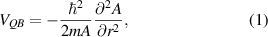
This quantization has been known for a great many years [39]. Over the intervening decades, there has been a search for methods of treating the quantum effects without having to solve Schrödinger's equation. As remarked above, one approach is to use an effective quantum potential [2]. If the wave function is written as  , then it has been suggested that the Bohm quantum potential is of the form [2, 50, 51]
where r is the direction in which the force is to be determined. If we use the previous relationship above between the density and the wave function, then this equation can be rewritten as (this follows directly with the substitution of the amplitude written as  ):
):
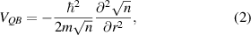
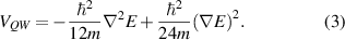
where n is the local density. This form is often called the density-gradient potential, and appears to have been first used in FET simulations by Grubin and Kreskovsky [64]. The compact form of this quantum potential means that it can be incorporated into a wide range of transport models for devices of many sorts, including MESFETs (metal-semiconductor FET [52]) and the MOSFET [65–67].
Wigner also introduced a form of effective potential, in his study of the impact of quantum mechanics on thermodynamics [68]. He found a pair of correction terms to the kinetic energy E in the form of a potential given by
If the normal thermodynamic form

where kB T is the thermal energy, is used, (3) becomes
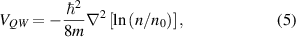
where  is a reference density. With a little manipulation, this latter form can be shown to be only a factor of 2 different from the density-gradient form (2) [69].
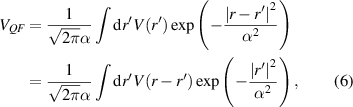
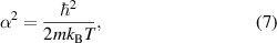
Still another form of quantum potential modification arose from the study of the non-zero size of an electron in a semiconductor [38]. In this case, it was shown that by considering the total energy of a potential (weighted by the density) in the Hamiltonian, the shape of the electron wave packet could be moved to the potential arising from Poisson's equation, which led to it being smoothed by [69]
where [70]
and the last line of (6) arises following a simple change of variables. As mentioned, this smooths the potential, especially in the region where the quantum well is located, and provides both the charge set-back and the quantization energy of the lowest subband [41]. This is shown in figure 2. It also can be shown to be equivalent to the above quantum potentials. To do this, the potential is expanded in a Taylor series around the position r, as follows [69]:

Figure 2. The triangular potential that normally sits at the interface forming the quantum well is shown in red. The effective form of this potential given by (6) is shown in blue. The charge setback is indicated by d and the quantization energy is indicated by ΔEC . Here, the vertical direction is energy and the horizontal is distance, with the oxide-semiconductor interface at the vertical jump in the red curve.
Download figure:
Standard image High-resolution imageThe first term is just the normal potential, and the next term vanishes upon integration, so that the leading term is the quantum correction which gives, in three dimensions
which is again within a constant of (5) when using (4). The point is that almost all of the various quantum potentials wind up being of the same form for small quantum effects, that is for small nonlocality. In figure 3, an example is shown comparing the Bohm potential (2) and the total effective potential (6) [71]. The structure is similar to a MESFET, in that the short barrier that creates the quantum point contact at the bottom of the structure is similar to a very short gate. In panel (a), the Bohm potential is created after solving for the full quantum waves in the structure in the absence of a self-consistent potential, and particle transport through the structure is indicated by the light stream-lines. In panel (b), both the Schrödinger and Poisson equations are solved self-consistently, and the Bohm potential is found, and particle transport is then determined. In panel (c), only the Poisson equation is used for the self-consistent potential, and the effective potential is computed from (6) and used to study the particle motion. In this latter method, there are far more vortices beginning to form in the transport, as there is more confinement observable in this method, as it is non-perturbative.

Figure 3. Particle trajectories through a gate defined quantum point contact. In each case, the density is found from the quantum wave functions for the structure. (a) With no Poisson solution, only the Bohm potential derived from the wave functions according to (2) is used to guide the particles. (b) Both Schrödinger and Poisson solutions are now used with the Bohm potential (2). (c) With both Schrödinger and Poisson solutions, the effective potential (6) is used to guide the particles. Reprinted from [71], Copyright (2000), with permission from Elsevier.
Download figure:
Standard image High-resolution image2.2. Tensile strain
When strain is added to a device, with the intent to modify the transport properties by modifying the band structure, it becomes a quantum effect [22, 23]. In the case of the n-channel MOSFET, the strain is tensile and often accomplished by putting a Si3N4 layer over the gate stack. This tries to stretch the channel. It was remarked in the previous section that quantization in the inversion layer separated the six-fold conduction band into a two-fold set of elliptical energy surfaces whose major axis is normal to the interface and a four-fold set whose minor axis is normal to the interface. Unfortunately, this separation is not particularly large, especially in elevated temperatures. The use of tensile strain increases this separation so that the conduction is dominated by the two-fold pair of sub-bands. A 1% uniaxial strain along the [110] transport direction can give as much as 70 meV splitting between the two sets of valleys [72]. Here, the effective mass for transport in the channel becomes the transverse mass, (∼0.19m0 in Si). This results in an approximately 40% reduction in the transport mass relative to the normal conductivity mass in Si, although the strain will affect this mass [73]. In addition, the carrier scattering between the two-fold and four-fold sets of valleys is greatly reduced, and these two effects together lead to a much higher mobility for the carriers in the inversion channel. Because these valleys are anisotropic, the actual motion in the channel can be quite complicated [74].
In figure 4, the effect of strain on the mobility is plotted for an n-channel device on the (001) surface of Si with the uniaxial strain along the [110] direction [23]. The strain deforms the normally circularly symmetric shape of the two-fold valleys, as can be seen in the figure. Several different levels of strain are given by different curves, and one can see that the mobility, though larger, becomes anisotropic in the valleys. Here, the effect of strain on the bands was calculated with an empirical pseudopotential method, and the transport was simulated with an ensemble Monte Carlo method. The results are comparable to what is seen experimentally in such devices. The result of warping of the ellipsoidal energy surfaces is quite expected in the understanding of these devices. The elongation of the normally circular energy surface in the plane of the device, causes a decrease in the effective mass in the channel direction.

Figure 4. Mobility enhancement for uniaxial stress applied along the (110) direction. The piezoelectric effect is also included in this enhancement. The horizontal axis is the same as the vertical. Reprinted from [23], Copyright (2008), with permission from Elsevier.
Download figure:
Standard image High-resolution imageNote that figure 4 actually plots the mobility as a function of the direction, and not the energy surfaces. Strain along a [110] direction elongates the crystal in that direction. Since momentum is proportional to the inverse of the lattice constant, this compresses the normal energy circle, so that the long axis of the constant energy line would lie along ![$\left[ {\bar 110} \right]$](https://content.cld.iop.org/journals/0268-1242/37/4/043001/revision2/sstac4405ieqn6.gif) , which is normal to the strain. Then, if the resulting constant energy line is written as
, which is normal to the strain. Then, if the resulting constant energy line is written as
the fact that the major axis in the ellipse is normal to the strain direction implies that

As a result, the mass in the strain direction is reduced, while the normal direction has an increased mass, a result in keeping with the theoretical calculations [23]. This leads to a larger mobility in the strain direction, as is indicated in figure 4.
While the two valleys in the lowest sub-band are normally degenerate, quantum interactions between carriers in these two valleys can lead to their splitting, which has been observed experimentally [75]. It has been found that the strain applied along the [110] direction, and the warping of the energy surfaces in the plane can lead to significant splitting of the these two valleys, while maintaining a coupling. The resulting energy surfaces are quite dramatic, as shown in figure 5 [76]. Here, the structure was computed using a  method, including the strain, and the dispersion is seen to become very non-parabolic [77]. Another important aspect is that the effects can become stronger in ultrathin layers of Si, such as in SOI or nanosheets [78, 79].
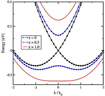
Figure 5. Dispersion of the two degenerate valleys normal to the (001) surface as a result of strain. The point k0 is the normal point along Δ near the X point. With the strain along [110], the dispersion becomes highly non-parabolic. Reprinted from [76], Copyright (2008), with permission from Elsevier.
Download figure:
Standard image High-resolution imageMore than 30 years have passed since SiGe alloys were suggested for use in semiconductor devices [80]. If the SiGe alloy is relaxed, then a subsequent thin Si layer will be under tensile strain. This was thought to be a good method of improving the transport [81]. This would lead to its use in hole transport.
2.3. Compressive strain
In opposition to the strained Si above, growing a strained SiGe layer on Si would put this layer in compressive stress, and using a subsequent Si layer on top would bury the SiGe layer as a quantum well [82]. The top Si cap layer moves the holes away from the surface as a means to reduce the surface-roughness scattering, while the strain in the SiGe layer splits the light and heavy-hole bands at Γ, providing a reduced transport effective mass. A drawback is that the SiGe layer has significant alloy scattering which tends to lower the mobility, so that there are competing effects. To generally describe the valence band structure, in both the quantum effects and with strain, requires a form of full-band calculation for the complicated splitting, warping and crossing of the various valence bands [83].
The approach to p-channel devices more or less settled upon the use of SiGe in the source and drain regions, where the larger lattice constant put the channel under compressive strain [22]. This uniaxial compression raises the light-hole band extremum above the heavy-hole band, so that the effective mass of holes becomes much smaller and the mobility is raised. This creates a problem, in that the two bands will now cross at a not too high value of carrier energy. They do actually cross, but hybridize in a manner to avoid this crossing; the result nevertheless is a very non-parabolic behavior with the initial light mass getting very large as the carrier energy increases. To understand this better, the normal unstrained valence bands in Si are shown in figure 6, along with an equal energy surface for the two top bands [84]. One can understand the phrase 'warping' from the two constant energy surfaces. The maximal extension of the heavy-hole surface is along the (111) directions, while that of the light-hole surface is along the (100) directions.

Figure 6. A schematic view of the valence bands in unstrained Si. E1 is the heavy-hole band, while E2 is the light-hole band. Δ0 is the spin-orbit split-off band. The constant energy surfaces near k = 0 are shown pictorially on the left. Reprinted from [84], Copyright (2008), with permission from Elsevier.
Download figure:
Standard image High-resolution imageThe energy surfaces in figure 6 are at very low energy. As the energy increases, the warping becomes much more pronounced, as can be seen in figure 7 for the unstressed bands (the upper row is the upper band after hybridization while the lower row is for the lower band). As the channels are normally in the [110] direction, the holes will see a much reduced effective mass and therefore an enhanced mobility.

Figure 7. The constant energy surfaces at 39 meV in the strained and unstrained case. It may be seen that the mass in the [110] direction is dramatically reduced as the strain is increased. Reprinted from [84], Copyright (2006), with permission from Elsevier.
Download figure:
Standard image High-resolution imageThe effect of the strain and the gate field can be observed in figure 8, where it can be seen that the gate field really has little effect on the constant energy surface for the dominant band [85]. Here, the lowest energy sub-bands are shown for both the strained and unstrained energy surfaces, as calculated with a  method. As the surfaces are not affected by the gate field, the masses similarly are not affected. Similar calculations for the valence band structure in the presence of the uniaxial strain along [110] have been done by Shifren et al [86], Wang et al [87], and Kotlyar et al [88], among others.

Figure 8. The constant energy surface of the lowest hole sub-band for the Si (001) surface devices, with the compressive strain along [110], for several different gate fields. The black curves and data points are for unstrained channels, while the red curves and data points are for the strained channels. Reprinted from [84], Copyright (2006), with permission from Elsevier.
Download figure:
Standard image High-resolution image2.4. Discrete impurities
The problem with fluctuations in the number of impurities under the gate was discussed already by Keyes [28] half a century ago. The actual distribution of the impurities cannot be controlled, and fluctuations in the actual number lead to fluctuations in the threshold voltages. In large devices, this fluctuation is small, but in small devices, it becomes much more significant. For example, if we consider a 10 × 10 × 10 nm region with a doping of 1019 cm−3, there are only 10 ± 3 dopant atoms in this volume. Hence, as devices become small, the fluctuations become large (30% in this example).
Attention was called to this again when Wong and Taur included the atomistic nature of these impurities in their MOSFET simulations [89]. The importance of this was quickly realized and picked up in the simulations of MESFETs and HEMTs [90, 91]. In figure 9, simulations of 16 different MESFETs of nominally the same dimensions and doping profiles and 18 HEMTs are shown, where the drain current is plotted as a function of the actual number of dopants under the gate, although the doping level is kept constant. It can be seen that the variation of the current with dopant number is not monotonic and fluctuates dramatically.

Figure 9. The drain current in simulations of MESFETs and HEMTs as a function of the actual number of dopants under the gate. © [1994] IEEE. Reprinted, with permission, from [91].
Download figure:
Standard image High-resolution imageThe inclusion of the actual positions of the random doping distributions was adopted widely in the simulation of MOSFETs as well [92–95]. In figure 10, the variation caused by the atomistic doping is illustrated by plotting the drain current as a function of gate voltage for a great many different implementations of a 0.1 μm gate length MOSFET, doped to 8 × 10¹⁷ in the substrate [93]. The fact that the current varies by more than an order of magnitude in the sub-threshold region points to the importance of this effect. It also became evident that impurities near the source-gate entry point into the channel affected the current far more than impurities further from this region [96].

Figure 10. Drain current for a great many different simulatons (differing by the random position of the dopants) for a 0.1 μm MOSFET. © [1998] IEEE. Reprinted, with permission, from [93].
Download figure:
Standard image High-resolution imageThe rise in these fluctuations has led to the ideas that the best course in past few years has been to not add any doping in the substrate, but let the channel appear similar to a n+ –i–n+ structure. With operation below 1 V, adequate voltage separation from the substrate can be achieved especially with double-gate FinFET type devices. A name of junctionless devices was coined some time ago [97].
While the fluctuations are important, it should also be recognized that an individual impurity can have a significant effect on the current due to quantum transport behavior. In figure 11, simulations of the behavior of a single [98] electron nearing a single impurity in the MOSFET channel are shown for various times. Here, the electron is represented as Gaussian wave packet (the size of the electron and these wave packets were discussed above in section 2.1). The right hand column is for a classical Boltzmann solution. The wave packet expands somewhat, which is normal for Gaussian packets, and moves deeper into the channel as it is repelled from the impurity. On the left hand panel though, the wave function becomes quite broken up due to the quantum interference, that leads to decoherence of the packet.
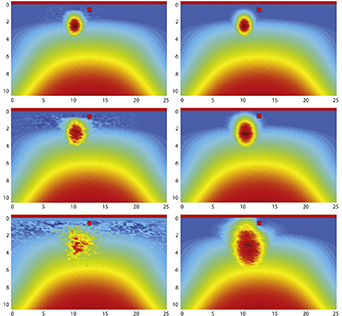
Figure 11. Comparison of classical and quantum Wigner function behavior of a single electron approaching a single impurity in a 25 nm MOSFET. The top row is 2 fs after the start, the middle row is 4 fs, and the bottom row is 8 fs after the start of the simulation. Red is high amplitude, and blue is low amplitude. Reprinted from [98], Copyright (2014), with permission from Elsevier.
Download figure:
Standard image High-resolution imageBut, the impurity can have a larger effect. The reader should be familiar with Young's two-slit optical experiment [99]. It can be replicated with electrons. A charged wire in a transmission electron microscope (TEM) creates what is known as a bi-prism, and electrons split as they pass this wire and form an interference pattern [100] just as that of photons in the Young experiment. Importantly, a single electron in the TEM, or a single photon [101], will lead to the interference pattern. That is, the single electron (or photon) must have both wave and particle properties, as recognized by Einstein [102]. For the purpose here, these observations mean that a single electron passing by a single impurity can create an interference pattern representing its wave-like self-interactions in diffracting around the impurity.
Two electrons and two impurities provide a complicated wave interaction process that illustrates the interference principle. Consider a simple nanowire structure with two repulsive impurities embedded in it, as shown in figure 12 [54]. Here, the nanowires are 40 nm wide, and the area of interest is some 60 nm long. The impurities are located at the two green circles, which are constant energy lines. The electrons are continually injected at y = 0, x = 20 nm, and absorbed completely at y = 60 nm. Consecutive injections are considered as independent, identically distributed statistical experiments, giving rise to the stationary distribution of a single electron. These electrons are simulated by a Wigner function wave packet (Wigner functions are covered in part 3 below). The continual injection allows the study of the steady-state inference with impurities. The electrons are injected at an energy of 0.14 meV, which is above the second transverse sub-band in the nanowire. This, plus the nonlocal interaction with the impurities leads to the injected carriers forming the two beams apparent in the figure in the region before the impurities (the carriers travel from bottom to top in the figure). The carrier 'density' from  is plotted in the figure. It is clear that the electron is diffracted by the impurities, and then interferes with itself downstream from them. This would be present even if only a single impurity were present. The interference peak evolves all the wave to the exit of the nanowire. These interference peaks are certainly reminiscent of the two-slit experiment.

Figure 12. Quantum electron density distribution of an initial wave packet, injected at x = 20, y = 0. The green circles are equal energy lines at 0.175 eV of the repulsive impurity potential. Reproduced from [54]. CC BY 4.0.
Download figure:
Standard image High-resolution imageAn analytical study of similar scattering with a single impurity has been done by Barker [103]. In this work, it is clear that the interference arises from the matrix element itself for the scattering interaction. Yet, the result shows almost the same interference pattern as figure 12, but with a few amplitude differences. For example, in Barker's work, the amplitudes of the different beams decay from the peak for the forward beam. In figure 12, the second beam to either side is weaker and this is likely the result of having two impurities in which their second beams tend to interact negatively to reduce this amplitude. Nevertheless, it is apparent from these, and other sources, that the quantum interference around an impurity is a real event that will influence nano-scale devices. Indeed, a study of the electron wave on its own when near its donor atom shows a quite complicated wave function that is dependent upon the presence of strain in the system [104].
The interference that appears with one or a few impurities becomes much more complex when many impurities are present [55]. The impurities lead to a random potential, which if sufficiently large can localize a number of the band states [105]. But, the random potential has another effect. Transport through the random potential is quite sensitive to the position of the Fermi level and the presence of any magnetic field, even the self-magnetic field of the current in the FET channel. Small variations in these quantities can lead to large variations in the conductance through the channel, and even chaotic behavior. These fluctuations are typically referred to as universal conductance fluctuations, and have been observed in a large Si MOSFET at low temperatures [106]. In small modern devices, this can lead to significant current fluctuations in the drain characteristics if there is insufficient scattering in the channel [107]. This will be seen below in figure 15(a).
Even when there is adequate scattering, current filaments can form in the channel [108], as shown in figure 13 for an n-channel, 50 nm MOSFET. In the figure, the channel runs from 50 to 100 nm, and the current is in A cm−2. The doping in the channel was 5 × 1017 cm−2, while the source and drain were doped to 2 × 1019 cm−2. The individual dopants are shown as dots or small circles, while the size of the circle corresponds to the depth below the surface of the impurity. The impurities are treated in real space by a molecular dynamics approach in which the impurity potential is split into a long-range part which appears in the Poisson equation and a short-range part treated by the direct molecular dynamics forces between the electrons and impurities [109]. An interesting effect is that the current filaments do not really break up and decohere until almost 40 nm into the drain region!

Figure 13. Current inhomgeneity in an n-channel, 50 nm gate length MOSFET, the details of which are in the text. The current scale on the right is in A cm−2.
Download figure:
Standard image High-resolution imageThese effects are often grouped under the heading of excess noise in experimental studies [110, 111]. As the localized states can be interpreted as traps, the fluctuations often appear as trapping/detrapping effects [112–114]. And, often the fluctuations are coupled to those from the random interface potential due to surface roughness [115].
2.5. Short-channel effects
One of the oldest problems in FETs is drain-induced barrier lowering [116]. In this process, a potential applied to the drain of the device affects the injected current at the source-gate barrier, thus leading to an increase in current with drain potential in a region where saturation is supposed to occur. It is not well appreciated that this effect will be dramatically increased when the transport becomes ballistic, that is when there is insufficient scattering in the channel of the FET.
Ballistic transport in semiconductors also is a relatively old idea. In the strictest sense, ballistic transport means the lack of any scattering. It is often discussed in mesoscopic structures, where the mean free path is comparable to the device size, in connection with the Landauer formula [117], but the ideas of ballistic transport are older, and derive from the earliest discussion of vacuum diodes. The Langmuir–Child law describes the ballistic transport of electrons in a thermionic diode, with space charge built up near the cathode (corresponding to our source in a MOSFET) [118, 119]. More recently, Shur and Eastman suggested that ballistic transport in ultra-short channel length semiconductor devices would have the same space charge and current relationship as the diode [120]. Drain-induced barrier lowering is one of the first indications of ballistic behavior [121], and leads to qualitatively similar curves.
However, one cannot argue just from the shape of the curves that ballistic transport is present, but must carry out the comparison with, and without, scattering as done in [122]. The impact of ballistic transport can be seen from a normal derivation of the current in a MOSFET, where
where Cox
is the gate oxide capacitance, L is the channel length, VG
and VD
are the gate and drain potentials, W is the gate width, v is the velocity along the channel, and Vy
is the surface voltage along the channel. Normally, one would now introduce the mobility, but in the case of ballistic transport this has no meaning. Rather, the velocity is a function of the local potential as  . In the ballistic case, the potential can be described through [119]
Introducing this into (12), one finds that saturation occurs in the same manner, but that
Hence, the appearance of saturation has little to do with the properties of the transport in the channel, although the voltage dependence of the current does change somewhat [123]. But, this result arises entirely because it is assumed that pinchoff does occur in the channel. The Langmuir–Child law for diodes does not have any restrictions on the carrier motion, such as occur with pinchoff. If the pinchoff restriction is removed, then one might well expect diode/triode like behavior in the MOSFET, especially under quantum conditions.
In materials like InAs, the transport length for the transition from ballistic to resistive transport can be 15–20 nm at room temperature [124]. Yet, this is sufficiently long to affect the device characteristics as is evident in figure 14, which is a quantum simulation of a 30 nm gate length InAs nanowire MOSFET [125]. The cross-section of the channel is 9 × 8.5 nm, and the channel region is undoped. It is clear that this device has some strange behavior in the gate characteristics near turn-on, and does not saturate in the normal manner. Studies of the transport itself confirm that it is almost completely ballistic in nature. This can explain the diode/triode like behavior of the drain current.

Figure 14. (a) Gate characteristics for two different 30 nm InAs MOSFETs. (b) Drain characteristics for one of the devices with a gate voltage of 0.4 V. Reprinted from [125], with the permission of AIP Publishing.
Download figure:
Standard image High-resolution imageBut ballistic transport is only one of the effects that arise in short channels. When the transport is fully quantum, then the transitions from the low-dimensional channel to the larger three-dimensional source and drain begin to play a role. When crossing one of these latter interfaces, there is a discontinuity in the carrier momentum, and since this occurs at both source and drain, the possibility arises for quasi-bound states, often called resonances, in the longitudinal wave function for carriers in the channel. That is, at certain biases, the drain current can have large peaks that are almost like resonant tunneling peaks. These may be seen in figure 15, which is a quantum simulation for ballistic transport in a 9.8 nm channel length Si MOSFET [126]. The channel cross-section is 18.5 nm wide and 6.5 nm in depth. The channel area is doped p-type with 5 × 1018 cm-3 concentration. In panel (a), the gate characteristics are shown for six different device doping configurations; the dopants are randomly placed according to the doping concentration and the grid size in the simulation. The peaks are the random fluctuations discussed above for atomistic doping when only a few dopants are present. There are, on average, only six dopants in the channel, so that their exact positions will introduce considerable variability. In panel (b), the drain characteristics are shown for a single device. While the small fluctuations are dopant caused, the large peaks are the result of longitudinal resonant levels arising from the mis-matches at the source and drain transitions. In a sense, these can be considered as source-drain resonant tunneling.

Figure 15. (a) Gate characteristics for six devices. The fluctuations are caused by the interferences due to the random positions of the dopants, discussed in section 2.4. (b) Drain characteristics for one device. The smaller fluctuations are due to the dopants, but the large peaks are longitudinal resonances. © [2005] IEEE. Reprinted, with permission, from [126].
Download figure:
Standard image High-resolution image2.6. FinFETs
The long road to FinFETs began many decades ago when it was realized that the danger of scaling would be seen in a situation in which the standby 'off' current of a chip was larger than the operating current. The road to FinFETs can largely be said to be a road in which control of the off current was the leading concept. The off current arises from the bipolar like nature of the n+ –p–n+ doping of a standard n-channel MOSFET (the complement is true for the p-channel). Much of the leakage current that provides the off current is a weak bipolar behavior in which the substrate plays an important part. The first step along the road was the concept of silicon-on-insulator (SOI) [128], as a means to suppress the substrate contribution to the off current. Indeed, the first chip appeared with this technology shortly after [129], and it was shown that these transistors did have a better sub-threshold slope (reduced leakage) [130].
The next step to control was the double-gate MOSFET, with top and bottom gates to better control the pinchoff [131]. But, this was a complicated and expensive fabrication process, so others began to look at different gate configurations that offered similar control [132, 133]. Thus was the arrival of the FinFET in which the channel is turned to the vertical direction with gates on either side. A variant was called the tri-gate transistor, shown in figure 16 [127], although gate materials have changed since this time [134].

Figure 16. Schematic of a tri-gate transistor. Reprinted from [127], Copyright (2003), with permission from Elsevier.
Download figure:
Standard image High-resolution imageTurning the channel vertical allows the surrounding gates to work together to dramatically reduce the off current in these devices. Nevertheless, new roughness appears due to fluctuations in the body thickness, essentially, the fin thickness [135]. Despite many perceived problems and various approaches, it was shown that the trigate design was a more scalable transistor than the conventional planar MOSFET [136]. In 2009, integrated circuits using the FinFETs and trigate FETs began to appear [137], although there were still experiments using alternative materials to Si [138]. Nevertheless, Intel introduced the trigate as a mainstream device at the 22 nm node in 2011, and the industry has not looked back.
With the gate potential on either side of the fin, turnoff of the transistor becomes more effective as these two potentials work together to shut off the channel. The normal state in which there are two inversion layers, one on either side of the fin, can change into a single inversion layer in the bulk of the fin. When the fin is sufficiently thin and the density is not too high, this central inversion layer is the preferred state [42]. Thus, the quantum effects can change the basic nature of the FET, from a surface-oriented device to a bulk-oriented device, which has the added benefit of less scattering from the rough interfaces. In figure 17, the charge density is plotted as a function of the fin width, for a total inversion density of 3 × 1012 cm−2. For smaller fins, one gets bulk inversion as opposed to surface inversion. Of course, larger gate voltages also pull the charge to the surface, enhancing surface inversion.
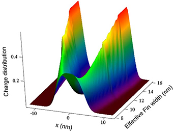
Figure 17. The charge distribution along the fin width (x direction) as a function of the fin width. For small fin width, one gets volume inversion, while for larger fin widths, surface inversion is found as expected. Reprinted by permission from Springer Nature Customer Service Centre GmbH: Springer, Journal of Computational Electronics volume [42], Charge density variation with fin width in FinFETs: an application of supersymmetric quantum mechanics, Razib S. Shishir & D. K. Ferry, © 2008.
Download figure:
Standard image High-resolution imageEven though one has better gate control in the FinFet, it should not be assumed that random doping effects will go away. This is just not in the cards [139], although here it seems that the devices are most sensitive to dopants in mid-channel. However, it does appear that the device is less sensitive to short-channel effects, and have low 1/f noise [140].
2.7. Nanowires and nanosheets
Once the concept of multiple gates was brought forward, then thoughts turned to what could be done with quantum wires, and a gate-all-around (GAA) technology. The first quantum wire device was simply a very narrow channel MOSFET, of 10 nm width [141]. The announced purpose of the device was to begin to study quantum effects in ultra-small MOSFETs, although the SOI device had a gate length of 250 nm, and the Si layer was 7 nm. The channel doping was only 1015 cm–3, so that there was typically no dopants in the channel, although they studied a range of channel widths (1.25–43.75 nm). They observed an increase in threshold voltage as the channel width was reduced below ∼10 nm. Simulations of these devices soon appeared [142, 143].
The GAA Si nanowires seem to have appeared both theoretically [144] and experimentally [145] around 2004. The fabricated wires were about 12 nm high and 20 nm wide, nominal gate lengths of 100 nm, and were surrounded with oxide, although the gate was closer to a trigate than a GAA. These showed excellent sub-threshold slopes, comparable to a large planar device. In simulation, it was shown that these devices had the same bulk-to-surface channel effects, discussed above for the FinFETs, with varying diameter wires [144]. In addition, these simulations did not show any increase in mobility in these nanowires. More advanced forms of simulation continued to appear [146].
It was pointed out Moore's law results from an economic law rather than a technology law [16, 17]. The economics boils down to the cost of Si itself, and leads to the fact that, for Moore's Law to proceed, the gate periphery must be larger than the Si area in order to minimize Si cost, as the technology proceeds. This certainly supports the transition to FinFETs. But, it was shown that nanowires laid on the surface of Si could not satisfy this economic requirement, and could not compete with FinFETs [147]. This is because you basically cannot pack a single layer of circular wires dense enough to overcome the height advantage of the FinFET. An alternative would be to have the wires vertical [16], but that is a more difficult manufacturing technology. Of course, a better way was found, and this is stacked nanowires [148, 149]. The nanowire stack was good, but it was not that much preferred to the FinFET. This changed with the nano-sheet FET, which was a stack of squashed wires—the vertical thickness was much less than the width of each wire [150], although the phrase nano-sheet would come later [151], in a joint effort of IBM, Samsung, and Global Foundries.
By utilizing other materials, such as SiGe and Ge, a range of strain possibilities arise in these GAA stacked devices [152, 153]. Generally, the substrate under the stack can undergo punch-through by the source-drain bias which leads to leakage, so that some form of punch-through stopping layer is used [154]. Later, the use of a bottom oxide was used to provide this behavior and to give better control [155]. In figure 18, a nanosheet stack is shown [156]. Although this stack has four nano-sheets, the usual and preferred, is to use only three nano-sheets. Use of the oxide led to better sub-threshold slope and less drain-induced barrier lowering.

Figure 18. Three-dimensional scheme and cross-section of the multi-nanosheet FET. (a) Transistor with bottom oxide. (b) Transistor with no bottom oxide. Reproduced from [156]. CC BY 4.0.
Download figure:
Standard image High-resolution imageThis has led to the announcement this year of IBM's 2 nm node technology using their nano-sheets and oxide spacer layers [157]. In this approach, the nanosheets are 40 nm wide and 5 nm thick, with an effective gate length of 12 nm. It is expected that this technology will appear in mainline production in 2024. But, other technologies are being examined for the nanosheets, since these are formulated by various epitaxial and deposition methods. Indeed, nano-sheets have been studied in the III–Vs, as mentioned above [138]. More recently, the monolayer transition-metal di-chalcogenides (TMDC) have been studied in this association [158]. Materials such as MoS2 and WS2 offer the ultimate in nano-sheets, as the layer is a two-dimensional material less than a nm in thickness. These materials have a sizable band gap and reasonable velocities and mobilities [159, 160].
Perhaps as important is the problem of keeping the n-channel and p-channel transistors of the CMOS pair close together. One suggestion has led to a variety of approaches that lead to perhaps stacking the n and p devices on top of one another as part of the nanosheet stack [161, 162]. One approach to this is the forksheet technology which utilizes a self-aligned common gate between the two devices.
2.8. Spin field-effect transistors (Spin-FETs)
The Spin-FET was theoretically predicted over 30 years ago [163] (for relevant reviews see, e.g. [56, 164–166]). This particular type of transistor uses the spin properties of electrons for switching. In essence, a Spin-FET is based on two ferromagnetic contacts (source and drain) connected by a semiconductor channel. Spin-polarized electrons are injected via the source contact into the semiconductor region. The manifesting channel current is modulated by the gate-voltage-dependent spin–orbit interaction [167] which results in electron spin precession during transport. The drain contact's magnetization acts as a filter, as only spin-aligned electrons can pass through. All ballistic electrons have the same spin rotation at the end of the channel, which is linked to the spin–orbit field dependence on the electron momentum. As a consequence, the spin–orbit interaction strength dictates the minimum required length of the semiconductor channel for sufficient spin precession. In principal, two dominant spin-orbit interaction mechanisms are known: Rashba (geometrically induced structural asymmetry [167]) and Dresselhaus (bulk inversion symmetry breaking [168]). In silicon thin films spin–orbit interaction is Dresselhaus-dominated [169, 170], and is due to interfacial-induced breaking of the inversion symmetry (for transport modeling see, e.g. [171, 172]). The spin–orbit interaction strength depends almost linearly on the effective electric field and has been reported to be in the order of 2 μeV nm [173], making confined silicon structures candidates for Spin-FET channels ([100] oriented thin silicon film channels seem to be those best suited [174, 175]). However, among the challenges is the fact that a channel length in the order of micrometers is necessary. This requirement is contradictory to the ongoing geometric device down-scaling. Modern semiconductor devices offer roughly two orders of magnitude shorter channels: a severe competitive disadvantage of silicon Spin-FETs. Moving forward, required channel lengths can, in principal, be reduced by increasing the gate-voltage-dependent spin–orbit field strength (e.g. III–V materials). Another challenge is electron-phonon scattering which introduces randomization and acts against the spin precession coherence. Tackling this challenge requires cryogenic operational temperatures, further limiting potential applicability of Spin-FETs. The original limitation of requiring ferromagnetic contacts by injecting spin-polarized electrons through electrostatically created point contacts has been overcome [176]. More recent work on Spin-FETs has investigated alternative channel (e.g. 2D materials) and electrode materials (e.g. cobalt) as well as multi-gate and multi-functional logic devices and systems (for recent reviews see, e.g. [165, 166]).
In 2015, researchers showed the first demonstration of a Spin-MOSFET with a high on/off ratio operating at room-temperature [177]. Two metallic ferromagnetic contacts (source and drain) are connected by a non-magnetic semiconductor channel, allowing for charge and spin transport. Parallel/antiparallel magnetization alignment between source and drain leads to a current increase/decrease at the drain contact respectively. The ability to change the contact magnetization of the contacts by an external magnetic field and/or by the current (spin-transfer torque) provides opportunities for reprogrammable logic [178]. A particularly important feature of Spin-MOSFETs is the fact that the contact magnetization is preserved without external power, partly enabling non-volatile logic devices. However, in contrast to Spin-FETs, spin orientation is solely determined by the injecting ferromagnetic contact orientation.
As a concluding remark on the matter of Spin-FETS, let us point out that from an efficiency point of view, Spin-FETs only hold true advantages over conventional transistor designs when no current flow is required for the fundamental transistor switching mechanism. Indeed, only if this switching mechanism is realized solely via spin manipulation, will Spin-FETs be able to advance to a high-impact transistor technology. For reviews of recent applications of Spin-FETs see in particular [165, 166].
2.9. Tunnel FETs
While the idea of tunneling in semiconductors is quite old, the idea of putting a tunnel junction into an FET seems to have appeared around 2007 [179]. At this time, the problem of poor sub-threshold slope and leakage current was becoming ever more important, and of course led to the rise of FinFETs and now nanowire FETs, as discussed previously. But, the idea of greatly improving the sub-threshold slope by using tunneling from the source into the channel was quite promising, and was quickly pursued by some [180, 181]. In this approach, a resonant tunneling structure is placed between the source and the channel, to create a large resistance in the sub-threshold region; but a smaller resistance through resonant tunneling as the device turns on. Interband tunneling from a p-source into an n-inversion channel did improve the sub-threshold slope. But there was a correlated problem with the device, and that was that the tunneling barrier lowered the available 'on' current in the device. This problem seems to be intrinsic to its very concept [182]. While there have been many approaches to try to raise the on current, including III–V materials [183] and monolayer compounds [184, 185], it does not appear that this problem has gone away. Almost immediately, it was suggested that graphene would be a suitable material for this device [184]. However, the device is still under study today, following ideas such as anisotropic insulators [186]. Yet introducing tunneling generally lowers device performance, in particular by limiting the available current that is intrinsic to a tunnel barrier, and this may be a problem not easily overcome.
3. Dealing with quantum transport
Quite generally, most engineers think of FET operation and performance in terms of the motion of electrons or holes, as well as the resulting space charge and self-consistent potentials [48]. This is simulated with classical or semi-classical methods. What then makes quantum transport approaches different? Certainly, the mathematics are somewhat different, and in certain cases much more complicated. But in reality, it is the physics and the physical effects that occur due to quantum mechanics that must be handled by quantum mechanics. Any quantum mechanical representation has to meet all the requirements of a self-contained and consistent mathematical theory, but it obviously also has to correctly reflect the laws of nature. In this sense, it is no different than classical simulations. But, the physical behavior is deeper.
The physical effects that arise have been outlined in the previous section. Of course, most of these effects, such as random dopants, appear in normal devices and are merely the result of the devices becoming smaller. Indeed, other quantum effects can be handled by modifications to the semi-classical transport of normal devices. This includes the quantum potential and/or the effective potential additions, and even the current striations that appear in figure 13 are basically classical. Thus, a great deal of the incorporation of modest quantum effects can be achieved without the complications of quantum transport.
However, this is not the case for the interference that is shown quite clearly in figures 12 and 15. And it is this interference, or correlation or entanglement, depending upon how one wishes to describe it, that is clearly evident in the device characteristics of figure 15. Interference is a property that is given to the electrons, or holes, when they are treated as waves under the premise of quantum transport. And this interference is not just the transverse quantization effect, but also the longitudinal resonances apparent in figure 15. Quantum interference and entanglement are some of the most important aspects of pure quantum transport [187]. It cannot be obtained with a semi-classical treatment of the particles. But there is more, as a detailed and careful look at figure 3 shows that there is a tendency toward the creation of vortices. A vortex is what you see as water runs down the drain, much in the fashion of whirlpools in the ocean. Vortices are well-known in classical hydrodynamics. Quantum waves create vortices as well, especially in the many-body interactions [188, 189], and many think of this as quantum hydrodynamics [190]. As may be expected, quantum vortices have a quantized angular momentum, which leads to more fluctuations as the vortices are created and annihilated. The quantization arises from the EBK (Einstein, Brillouin, and Keller [191–193]) form of quantization which leads to:
where n is an integer and h is Planck's constant. Surprisingly, this same equation comes into play for the Aharonov–Bohm effect [194], and in the spin-FET [195], both through the Berry phase [196]. In the full quantum world, the constant n can be modified in many circumstances. For example, it is known to become  in WKB approaches (Wenzel, Kramers, Brillouin [197]). In proper quantum mechanics, p becomes the expectation value of the momentum. Equation (15) can take on other values when topological considerations come into play, such as in spin effects. It is clear that this quantization can well be important in modern FETs, where quantum transport must differ from semi-classical transport in the FET. It is in the treatment of these truly quantum effects which lead to observable behavior. No perturbatively obtained extra potential can give rise to this interference behavior. Moreover, no perturbative treatment of impurity scattering, even in quantum mechanics, can show the interferences of figure 12. Much of this behavior can occur over regions the size of the thermal de Broglie wavelength [198]. In a Si MOSFET at room temperature, this length is a few nm. In the modern world, some feature sizes are much less than this, and quantum effects are expected to be prevalent in the transport through these modern devices.
There are basically four common approaches to the treatment of quantum transport. These are: (a) direct solution of the Schrödinger equation, (b) the density matrix, (c) non-equilibrium Green's functions (NEGF), and (d) Wigner functions. It is not the purpose here to treat these in depth. Rather, a brief introduction to each will be given and then examples will be given that demonstrate how these approaches have been used to describe FETs. But first, it is important to review a few basics that are independent of the transport scheme used.
There are some general concepts for discussing the quantum effects that appear in FETs, whether they are experimental details or simulation descriptions. The first is described schematically in figure 19. In the figure, there are two domains. One is the physical domain of the device shown in the upper panel. The other is the simulation domain illustrated in the lower panel. The most important dimension here is the longitudinal coordinate along the current flow direction, which is taken to be the x-axis. It does not matter whether this is a planar FET (pictured) or a dual-gate FET or a gate-all-around nanowire FET, the descriptions will be the same. The simulation domain has been split into five distinct sections. The obvious ones are the gate, channel and drain, which are easily replicated by the physical design of the transistor. What is not so often recognized is that there are two transition regions, one between the source and the channel, and the second between the channel and the drain. These transition regions are extremely important, and they may be much larger than indicated in this simple drawing. For example, it has been shown that the high kinetic energy that carriers bring into the drain region may take as much as 20–30 nm to dissipate as the carriers thermalize [108]. Consequently, failure to carry the detailed simulation well into the drain may fail to give adequate recognition to this fact, and miss important device physics. The drain and source regions are not simply 'contacts'. Important quantization occurs in these regions, especially in the nanowire devices, and the transition regions have to relate this quantization to that occurring in the channel.

Figure 19. Two domains need to be considered in discussing the quantum transport. The first is the physical device domain (top) and the second is the simulation domain (bottom).
Download figure:
Standard image High-resolution imageThe second general problem is indicated in figure 20 where local potentials are plotted along the device longitudinal axis. In panel (a), the device schematic is repeated from figure 19, in order to position the potential relative to the device parts. In panel (b), the potential variation from source to drain is indicated in the absence of any bias. This variation is also present in the absence of dopants in the channel region (the so-called junction-free FET), but the amplitude is less than in a doped channel region. Finally, panel (c) indicates the potential variation when positive gate and drain voltages are applied. Note that the potential peak is less in this case due to the gate bias, as the latter meters carriers into the channel. It is important to note that the potential barriers, or the variation in potential along the channel require excess charge to be present. Thus, even in the absence of bias, the device is not in equilibrium, but in a sort of steady-state. The potential step at the source end requires a dipole of charge, whose size is determined by the width of the potential rise. These space-charge regions have to be fully accounted for in any simulation, as they provide both boundary conditions and physical transition limitations on the simulation. But they require even more from the quantum simulation [199].

Figure 20. (a) Device schematic from figure 19. (b) Potential variation along the device with no applied biases. (c) Potential energy variation with positive drain and gate voltages applied.
Download figure:
Standard image High-resolution imageIn the simulation domain, the quantum problem is usually partitioned into various parts, just as in the physical device. This partitioning was discussed in quantum theory at least as early as the work of Löwdin [200, 201]. One begins with the separate slice Hamiltonians that are the transverse eigen-states, and builds up the structure via couplings between the slices. In essence, the resulting system Hamiltonian is partitioned into sub-sections. For the schematic in figure 19, there will be five diagonal blocks, one each for the source, drain, channel, and the two transition regions. The off-diagonal blocks will describe the interactions between one region and its two neighbors. This general form is found in all four of the quantum simulation techniques mentioned above, although in many applications that have appeared, the two interaction regions have been relegated to the off-diagonal parts of the matrix. This is explained in a little more detail in figure 21 [202]. Here, the various slices that make up the device are shown in panel (a), while the total Hamiltonian is given in panel (b). There is a group of slices that correspond to each part of the device discussed in figure 19 (it should be mentioned that there are other methods to reduce the size of the Hamiltonian; in two dimensions one such is [203]). In this figure, the transitions may be considered to be the last electrode box closest to the device and the light grey boxes, coupled by Tdr or Tdl. The current through the device may be written as [202]
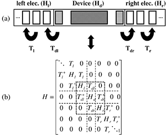
Figure 21. (a) Schematic representation of an 'atomic' system, in which the left and right electrodes are the source and drain respectively, and the device is the channel. Each block may be several layers thick, in which a layer is described by the quantized transverse states, which may themselves be built up from atomic wave functions. The couplings are indicated by the arrows. (b) The total Hamiltonian that results from the slice representation of (a). The central device is shown in the dashed box. Reprinted from [202], Copyright (2003), with permission from Elsevier.
Download figure:
Standard image High-resolution imagewhere the μ are the Fermi levels in the left and right contact regions, and Tlr is the transmission of a particular wave in the left contact (fully to the left so that that particular layer is nearly in equilibrium) to a particular wave in the right contact (again, fully to the right so that that particular layer is nearly in equilibrium).
It was emphasized by Landauer [117] that the transmission must be computed from the far left to the far right, and not just over the device region, in order to properly account for the role played by the charge dipoles mentioned above. Indeed, (16) may be immediately recognized as one form of the Landauer formula. While some feel that this formula is limited to low temperature ballistic systems, this is not the case. If properly applied, (16) is quite universal and even handles the presence of significant scattering. Thus, it is an important equation to keep in mind, as many, if not most, of the four methodologies for quantum transport will eventually use the Landauer formula. However in semiconductors, there is an additional change due to the fact that these are not metals. Hence we have to account for the fact that different modes can have different propagation velocities. This requires the modification of the transmission terms to
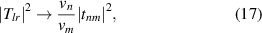
where this measures the transmission tnm from mode n on the left to mode m on the right, and summations over the modes must be made.
In principle, the entire matrix of figure 21(b) can be inverted to find the eigenvalues, but this can be expensive. For example, with a three dimensional device and a grid size of  , the order of this matrix is 106. This is solvable, but usually only with massive supercomputers. A more common method is to iterate the solution from the two ends. For example, beginning by solving just the Hamiltonian of the far left slice of figure 21(a). This would be just
  , or a matrix of order 104, which is considerably easier. This is discussed in the next few paragraphs. In either case, an important property of the system lies in the diagonalization of the germane Hamiltonian. It is needed, for example, in (16) where the transmission is computed for a mode, but Poisson's equation requires the amplitude at each site (the density at each site).
Another method that has some promising properties is the contact block reduction method (CBR) [204]. In this approach, all of the surrounding world is projected into the dashed box in figure 21(b). This greatly reduces the size of the matrix that has to be inverted, and this inversion is done only once. As this is usually applied to Green's functions, it will be discussed further when these are dealt with.
3.1. The Schrödinger equation
The normal approach to solving transport using the Schrödinger equation is straight from the textbook. This involves matching the wave function and its derivative at each slice of the structure (across the interface, as shown in figure 21). But, this is generally unstable when a large number of such interfaces are present, due to the presence of evanescent modes that must be accurately treated. This leads to both increasing and decreasing exponentials, and that is the source of the instability. Stability can be restored by modifying the recursion to one based upon the scattering matrix, which has long been a staple of microwave systems and entered quantum mechanics through the Lippmann–Schwinger equation [205]. The stability of this approach lies in the fact that modal solutions maintain their orthogonality through the scattering process [205]. In small devices, the connection to microwave theory becomes stronger as the transport becomes dominated by the modes introduced by the lateral confinement, much as in a microwave waveguide. The use of scattering states provides a method of building up an orthogonal ensemble, even with weighting of the states by e.g. a Fermi–Dirac distribution [206]. This is particularly useful for the initial conditions of the wave function in a particular semiconductor device [207]. In the end, this approach allows to determine the transmission from one end to the other and evaluate the conductance via the Landauer formula.
Normally, the transport would be governed by the size of the Hamiltonian. In the scattering matrix approach however, the matrix is twice that of the Hamiltonian due to the existence of waves traveling in both directions. These are separated to avoid the exponential problem of wave function matching. Thus, the modes and their momentum wave numbers are computed at the far left slice in figure 21, via the matrix [208–210]
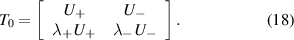
This is a scattering matrix form. Prior to this, the Hamiltonian for this first slice is solved to find the eigen-functions and the eigen-energies. The U matrices are then the similarity matrices for the forward and backward solutions for the wave functions, while the λ matrices are the eigen-value matrices. Normally, we think of the similarity matrices being the transformations on the Hamiltonian as

where I is a unit matrix. In other words, this matrix allows one to diagonalize the Hamiltonian, and find the eigen-values for the particular slice. Since, these eigen-values, for propagating waves, can correspond to forward or backward propagation for that particular slice, the system is doubled in dimension in order to separate the two types of eigen-values [208]. When the Hamiltonian is inverted to find the eigenvalues, a result is the similarity transformation matrix U, which is used to diagonalize it. This matrix is also computed during the process, and it (or its adjoint, depending upon the details of how one defines it—the order of matrices in (19)) contains valuable information. The columns of this matrix are the modes and their values at each site on the grid used to solve Schrödinger's equation. The rows are the values of the various modes at a particular grid point. This matrix is now a mode-to-site transformation matrix.
The matrix (18) changes the mode wave functions into the site wave functions in this zero-slice initialization of the process. Process through the structure is generated by solving the required normalization to a unit matrix of the following set of matrices [55, 57, 211]:
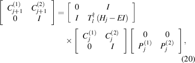
where the I are unit matrices.  and
and  are the amplitudes of the forward and backward modes respectively. The initial values of
  are determined as the value of the Fermi function in the far left slice (between 0 and 1), while
  . The P matrices will be found from the basic scattering matrix requirement that
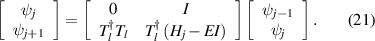
Equating these last two equations gives
These are now propagated to the Nth slice, which is the end of the device and Hr region, and then onto a terminating slice. For various points in the device, Tl will become Tdl, as indicated in figure 21. At this point, the inverse of the mode-to-site transformation matrix is applied to bring the solution back to the mode representation, so that the transmission coefficients of each mode can be computed. The density at each point in the device is determined from the wave function squared magnitude at that point, which is back propagated from the terminal so that the wave function at site i in slice j is given as

This solution technique for the direct Schrödinger equation was used for the MOSFET depicted in figures 14 and 15 above.
If there is no scattering, and the device transverse dimensions remain constant from one end to the other, then the various modes will be uncoupled, so one can simply use the Landauer formula. This provides a type of ballistic transport for a small device and has been used to study wave function penetration into the gate oxide [212], and to study a double-gate FET in TMDCs as a biological sensor [213]. A slightly different formulation, termed the quantum transmission boundary method [214], has been used to study the effect of defects in graphene nanoribbon FETs [215].
It is not necessary to avoid including scattering, as it can naturally be added via a self-energy correction [216] (the self-energy is discussed further below). Primarily, the scattering is represented by the imaginary part of the self-energy, and this was calculated for all common scattering processes [216]. With these scattering processes, the crossover from ballistic to collision-dominated transport (usually referred to as the ballistic-to-diffusive crossover) was studied for Si and for a variety of temperatures and materials [124, 216, 217]. Thus a direct solution method provides a viable simulation technique for FETs that can be done on a standard desktop computer and provides accurate representations of the quantum physics.
3.2. The density matrix
The second approach, which is one of the most straight-forward approaches, creates a matrix of modes. Generally, the Schrödinger equation is solved by assuming an expansion of the wave function in a suitable basis set so that each basis function is an energy eigen-function according to

just as is done for the regular solutions of the previous section. Here, En
is the energy level corresponding to the particular basis function  . For example, in a quantum well, the basis functions are the set of wave functions corresponding to the bound states of the quantum well. In a quantum wire, these are the bound states arising from the quantization resulting from the wire width (and height). In both of these cases, the basis functions are the mode wave functions. They have values on the sites of the grids used in the computation. Then, the total wave function can be written as
For the general situation, one may then define the density matrix, as a single time function, to be
The off-diagonal elements are rapidly oscillating in the difference frequency, so that they are usually ignored in transport theory. However, these off-diagonal elements are generated in the complex device and represent entanglement of the various modes, such as that occurring in figure 12 [218].
Generally, the device is embedded within an environment, such as shown in figure 21, and this environment can include other devices. So, the total Hamiltonian can be written as [31]

where the last term represents interactions between the device and its environment. Since measurements are always made in the environment [59], the coupling between the device and the environment is crucially important. The reduction to the dashed box in figure 21 can be achieved through the use of projection operators [219], in which the goal is to find the equation of motion for the reduced density matrix

The problem is that the equation of motion arises from the normal Liouville equation in which
where the last term defines the commutator relationship. It is to this equation that the projection operators are applied [31, 53, 57]. The details will not be presented here, as they are complicated and the result agrees with intuition. The end result is that the equation of motion for the device density matrix is found to be
where in the last term,  is the self-energy mentioned above and represents scattering within the device and between the device and its environment. The reduced interaction (represented by the overhead bar) in the first term represents effects of the environment on the device, such as boundary conditions affected by the environment.
There are two common approaches followed from here to obtain solution techniques of use for the solving of the properties of a device. In the first approach, a set of balanced equations for the density, momentum (current), and energy are obtained [220, 221], just as are normally done with the Boltzmann equation [222]. These equations are referred to as the (quantum) hydrodynamic equations. These equations were used to study tunneling in single and double-barrier structures [64, 223]. Often, these approaches bring the explicit quantization in a confined structure into the problem via an effective potential, and this approach was used to study the carrier density distributions in a GaAs HEMT [224].
It is possible to directly use the Liouville equation (28), and try to solve this equation directly. However, it is not obvious that one can do this for an application in a small semiconductor device. One problem is that we cannot just do the diagonal terms in the density matrix, but must also properly account for the off-diagonal terms [225]. But there is a long history of this approach [226]. The presence of the reservoirs, or contacts, generally lead to interferences that appear within the off-diagonal terms [227–230]. Indeed, this approach has been used to study the transport through a small  structure in Si [231, 232]. More recently, this approach has been applied to a double-gate ultra-thin-body Si MOSFET [233]. The channel region was 5 nm thick and 10 nm long, and lightly doped. The source and drain regions were more heavily doped. In figure 22, the potential throughout this device is shown. The effect of phonon scattering and interface roughness scattering are shown in the distribution functions in figure 23, where the diagonal terms of the density matrix are plotted as a function of energy.
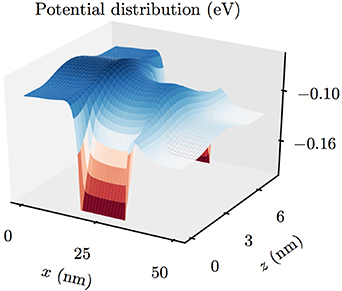
Figure 22. The potential in the 5 nm thick device. The reference level is the Fermi energy in the source region. Reprinted figure with permission from [233], Copyright (2020) by the American Physical Society.
Download figure:
Standard image High-resolution image
Figure 23. The diagonal elements of the density, plotted as a function of energy, for the source and drain of the device. The latter represents the final occupation for (a) phonon and (b) interface scattering. The solid and dashed red lines represent the expected ballistic occupation from source and drain, respectively. Reprinted figure with permission from [233], Copyright (2020) by the American Physical Society.
Download figure:
Standard image High-resolution imageThe second approach develops a proper quantum kinetic equation and then solves it directly for the density matrix, an approach that is amenable to using ensemble Monte Carlo particle methods [234]. The density matrix is more complicated than a classical approach as there are two positions and the time along either of these must be considered. But a path integral equation can be constructed from the equation of motion for the density matrix, and this serves as the basis for developing a Monte Carlo procedure. More importantly, this procedure is not limited to just the lowest-order scattering processes [235].
General Monte Carlo techniques coupled with the density matrix have been discussed by Jacoboni [236]. This approach was used to follow time-dependent wave packet trajectories, and the Bohm potential, in order to build up the density matrix [237]. Monte Carlo was also used with the density matrix to study interband tunneling of holes at high electric fields in GaN [238].
3.3. Nonequilibrium Green's functions
With the classical Boltzmann equation, one has a nearly equilibrium situation in which the distribution function is a Maxwellian or a Fermi–Dirac at a temperature possibly above that of the lattice. One often couples this with an assumption that the contacts are in near-equilibrium, but this is not always true, as was seen in figure 13, and this assumption is no more likely to be true in the quantum case. Then in the hot carrier system, and that means most devices, the distribution is unknown and has to to be found via one of several possible methods to solve this version of the Boltzmann equation, as the currents (and therefore the device characteristics) are found from integrals over this distribution.
In quantum mechanics, the system is quite the same, giving rise to excitations that propagate under the action of the potential. The NEGF include new functions that must be found to describe this very non-equilibrium distribution [239, 240]. With these Green's functions, the wave functions  and
and  go beyond the simple forms (25), as the coefficients become expressed as fermion creation and annihilation operators. Thus, the wave functions are referred to as field operators [57], and the Green's functions determine the transport of an excitation over a certain distance (given by the two positions and times in the arguments) to where it is annihilated (or destroyed). In this sense the Green's functions describe transport through the system. In terms of these two field operators, one uses the anti-commutators for fermions as

and the four Green's functions in NEGF are described by
Here,  and
and  are the retarded and advanced Green's functions respectively, and derive from the near equilibrium case where the distribution function is a Fermi–Dirac function. These define the spectral density as

where k and ω are Fourier transforms of  and
and  respectively. The spectral density relates the energy to the momentum of the quantum state. Classically, this is a delta function asserting that, for example
  , where the momentum
  and
and  is the effective mass in the semiconductor. In quantum mechanics, the presence of state broadening leads to a breakdown of this equality, thus leading to the need for the spectral density. These two Green's functions,
  and
and  , are operator expressions, hence the anti-commutation (curly) brackets common for fermions.
The other two Green's functions in (32) are not operators, but are correlation functions related to the distribution function that must be found for the non-equilibrium device. The connection between these two functions is not accurately known in the far from equilibrium case, but has been hypothesized to maintain the same form as found near equilibrium [240]. This ansatz thus gives the less-than function as [241]

and the greater-than function as

where  is the nonequilibrium distribution function. As one can infer from the multitude of functions, using the Green's functions is far more difficult than using either wave functions or the density matrix.
The correlation functions (34) and (35) require a pair of equations of motion for these quantities. With the added complications of having four functions, these equations will be more complicated than the simple Boltzmann equation. Keldysh [242] introduced a general method with a single matrix Green's function, and hence a single matrix equation to be solved. This does not reduce the overall effort required, but it simplifies the equations in which these functions are described. The Keldysh matrix involves a contour that defines the evolution of time between  and
and  , either forward or reverse in time. This contour is drawn from the initial time (t0 or 0) to the time of interest (the lower part of the overall contour) and then back to the initial time (the upper part of the contour). Each of these field operators can be on the upper line or the lower line of the overall matrix. The matrix is a 2 × 2 matrix. The wave functions enter the Green's functions through (32). The rows of the Keldysh matrix are defined by the operator
  . That is, row one of the matrix corresponds to when t is on the lower line, while row two is defined when t is on the upper line of the trajectory. Similarly, the operator
  defines the columns of the matrix. Column one is defined when
  is on the lower part of the trajectory, while column two is defined when
  is on the upper part of the trajectory. This is discussed fully in more detailed treatments [57], but is not all that germane to the discussion here. This contour ordered matrix may be written as:
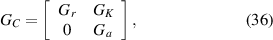
where the Keldysh function is

and  and
and  are given by the third and fourth lines of (32), respectively. From the Liouville equation (28), the equation of motion for the Green's functions can be written as [242]
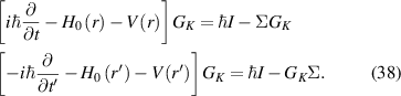
Here, the bold-face characters are the matrix forms following (36). The Keldysh approach and its failures will be discussed further in the
Most modern approaches to the use of NEGF for devices base their work on the Keldysh [242] formulation. The scattering self-energies  depend on the correlation functions
  and
and  and on the greater and lesser Green's functions of the phonons, which account for the occupancy of the phonon states and depend on the phonon energies. Keldysh himself uses the S-matrix from equilibrium theory that works only upon the assumption that the system is close to equilibrium, so that the normal techniques can be used. Keldysh also assumes the interaction representation, in which the scattering-derived
  is assumed to follow from a unitary time-translation operator. But this assumption fails when the energies contain self-energies so that the Hamiltonian is no longer Hermitian. More importantly, Danielewicz has pointed out that correlated initial conditions also make the S-matrix questionable at best [243].
The entire concept of the contour mentioned above is also debatable. When electric fields or forces are applied to the device, the entire complex system undergoes a phase transition that breaks time-reversal symmetry. The device, within its environment, then seeks a steady-state if it exists; a far-from-equilibrium stable state that balances the driving forces and the dissipative forces [53]. During the transient evolution to this stable state, the system may evolve though a number of intermediate phases: e.g. homogeneous, inhomogeneous, linear, nonlinear, etc. When these driving forces are removed, the system response does not reverse its course through these different phases, but seeks a relaxation toward the equilibrium steady-state from which it initially deviated. This excitation/relaxation cycle may involve significant hysteresis. The excitation process generates entropy [220]. The relaxation process does not remove this entropy from the system, but generates even more as dissipation still occurs during this relaxation. The adoption of a time-ordered contour that smoothly retraces itself to its initial state is contrary to this physics (discussed further in the
Many approaches to using the NEGF use this perturbation theory expansion to arrive at Σ, even in the case of impurity scattering. It has already been pointed out that this approach will not yield the interferences seen in figure 12. More properly, the terms  and
and  should be two-particle Green's functions, and their partition into a pair of single particle Green's functions is not clearly evident, as it ignores all correlations. The evaluation of a two-particle Green's function is usually much more complicated and cannot be reduced to a simple Dyson's equation. Rather, it needs the full evaluation of the Bethe-Salpeter polarization [57]
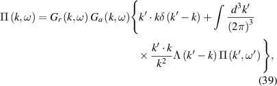
which then enters the conductivity as
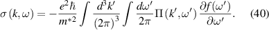
The distribution function  comes from (34). Failure to incorporate the Bethe–Salpeter equation should cause a questioning of results found with the use of NEGF.
Most approaches for actually solving for device response with NEGF rely on a version of the CBR mentioned above. With this approach, the Green's functions can be reduced to those of the device itself (the region in the dashed box in figure 21). The CBR leads to equations of the form [244]
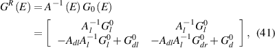
with

The subscripts are written according to figure 21. The matrix A can easily be evaluated using the properties of the self-energy, which is presumed to be non-zero only where the system makes contact with the external leads. This obviously means that ballistic transport is being assumed throughout the device. But in the case of ballistic transport, NEGF is an unnecessary afterthought. For ballistic transport, the coupling to leads gives the self-energies that define the transmission from one lead through the device to the next lead as [245]

and the trace over the matrix T is used in the Landauer equation (16). The Γ are the imaginarly parts of the self-energies that arise from Tdl and Tdr . Since the two Green's functions in this equation are the equilibrium Green's functions, use of NEGF seems to be overkill and is used more for hype than for need.
It is clear that the interference from impurities can be treated with NEGF from the earliest applications to real devices [103]. More recently, the role of fixed charges in Si nanowire FETs was examined, taking full account of the atomistic positions of the fixed charge within Poisson's equation (and not with perturbation theory) [246]. These authors clearly demonstrated how a few random dopants can greatly affect the nanowire FETs. The effect of random dopants in an InAs drain region for a Si tunnel FET was also examined [247]. Then, using DFT to calculate both the band structure and the full asymmetric wave functions of donor electrons in Si nanowire FETs, it was clearly established how this anisotropy could affect the transport properties [104].
NEGF was used early to study the properties of double-gate MOSFETs and showed that channel length modulation and drain-induced barrier lowering became significant for channel lengths below 15 nm [248]. It was also used to study a double-gate SOI Si MOSFET [249], and to study the role of phonon scattering in multi-material nanowire FETs and FinFETs [250]. In figure 24, the current spectra found in this latter work, overlaid on the potentials, are shown for two Si nanowire FETs of 2.2 × 2.2 N m2 and 3.6 × 3.6 N m2. It may be seen that the larger cross-section device has less change in the current. The hot electrons have not relaxed in this larger device even after 65 nm of drain region. It may be concluded from this that the denser density of states in the smaller wire has more dissipative scattering than the slightly larger wire, and that relaxation of the carriers extends well into the drain regions for quite a distance.

Figure 24. Current spectra taken for Si nanowire FETs of (top) 2.2 × 2.2 N m2 and (bottom) 36 × 3.6 N m2. The drain region is 64 nm in length and VG = 0.9 V. The dotted white line is the first subband and the dashed red line is the current-energy variation in the device (basically the integral over the cross-section of the product of current and kinetic energy). This dashed red line shows clearly that the hot carriers have relaxed even after 64 nm of drain. Reproduced from [250]. CC BY 4.0.
Download figure:
Standard image High-resolution imageOthers have also studied nanowire FETs of various types [251] and FinFETs [252], as well as various tunneling structures [253]. Strong simulation packages using full band structure and NEGF for transport have appeared for FETs over the years [254, 255]. There have been several studies of alternate material FETs, typically graphene and TMDCs, that have used NEGF as well.
3.4. Wigner functions
In classical physics one uses the Boltzmann equation, which yields a distribution function that is defined in position, momentum, and time. Hence, there has always been a desire to have a phase space formulation in quantum mechanics, and one was developed quite early by Wigner [68]. To approach this, and to clarify the two positions and time that appear in the density matrix, as well as the NEGF, the center-of-mass and difference coordinates are defined through
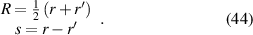
Like the density matrix, the Wigner function has only a single time, so that the times in NEGF are set equal as  . Then, the density matrix may be transformed on the difference coordinate as
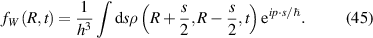
Using the Liouville equation (28), this leads to an equation of motion for the Wigner function that is expressed as (in one dimension)

where
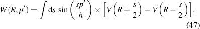
The term  is often called the Wigner potential. Scattering has not been included, but it is easily incorporated by a gain-loss term added to the right-hand side of the equation. This is usual for treatment of devices, and we will return to this below.
The Wigner function is not a positive definite function under far-from-equilibrium conditions [256]. This is a consequence of the uncertainty relationship. If the Wigner function is integrated over position or momentum, a positive definite function gives the probabilities (square magnitude of the wave functions) in momentum or position respectively. The negative excursions of the function exist over phase space regions whose volume is of order  (in three dimensions), so that smoothing the function over a volume corresponding to the uncertainty principle will produce a positive definite function. The Wigner function is always positive definite in the ground state appropriate to equilibrium. But the onset of negative excursions of the Wigner function are viewed as the appearance of correlation and/or entanglement [58]. Such correlation or entanglement is connected to off-diagonal elements of the density matrix [218], and these lead to oscillatory behavior in the Wigner function and the negative excursions. Because of the phase-space nature of the Wigner distribution, it is possible to identify where quantum corrections enter a problem by comparing it with the classical version. Wigner himself derived an effective quantum potential that can be used as a correction term for the potentials in thermodynamics [68]. It is worth remarking that many start their study of devices with NEGF, but finally resort to using the Wigner function [257].
As with Green's functions, early use of Wigner functions for transport considered resonant tunneling diodes [207, 258]. Such tunneling can be seen in figure 25, where a Gaussian wave packet is in the process of tunneling through a 3 nm AlGaAs barrier, with GaAs regions on either side [259]. The total wave packet still has components that represent the initial wave packet (on the right below the barrier, represented by the two black lines), the reflected wave (on the left below the barrier), and the transmitted wave (above the barrier). It is worth noting that a wave packet is composed of a great many waves, and the figure shows how the reflected components actually slow down and then accelerate into the backward direction. Reflection and transmission is not instantaneous in quantum mechanics, but occurs over a period of time, which is characteristic of the motion of the wave packet. The wave here is incident on the barrier at a slight angle, which is observed in the 'tilts' of the partial waves, and there is a small electric field applied which is apparent in the increasing momentum as the wave moves forward (upward).
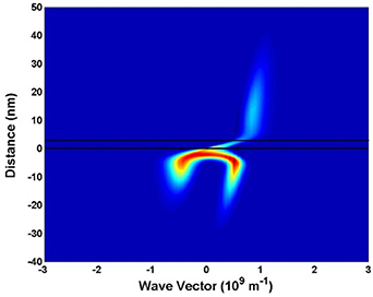
Figure 25. Tunneling of a Wigner wave packet through a 3 nm single barrier in the GaAs/AlGaAs system. The incident and transmitted partial waves have positive momentum, while the reflected wave has negative momentum. Reproduced with permission from [259].
Download figure:
Standard image High-resolution imageThe Wigner equation of motion (45) is quite similar to the Boltzmann equation, except for the complication of the Wigner potential, which arises from the nonlocal properties of quantum mechanics. Nevertheless, it is possible to transform the equation of motion into a path integral form, from which a Monte Carlo procedure can be developed. As has been mentioned in the Introduction, the idea of using particles in quantum mechanics was discussed quite early by Kennard [2]. The concept of a Wigner path is thus useful, as it provides a representation of the quantum evolution, and leads to numerical simulation of the Wigner equation of motion. Such a path is followed by a small sample of the Wigner function as it evolves through phase space (these are represented by the particles used in the simulation). Moreover, this path evolves quite like a classical particle, except for scattering and for rapidly varying quantum potentials, as described by Kennard [2] and later by Bohm [51]. Using paths guided by the Bohm potential has been used extensively by Oriols [260]. In using particle approaches with the Wigner function, there are a few quantum issues that have to be addressed. First is the problem of including interference effects leading to negative excursions for the Wigner function. Second will be the nonlocal effects that have to be treated in scattering processes, especially those that appear in treating FETs.
The problem of phase is dealt with first. An early approach used a weighted Monte Carlo in which each particle was assigned a particular weight [261]. A variant to include paths with negative weights handles the negative parts of the Wigner function [262]. Because some of the Monte Carlo particles carry negative weights, a problem arises as to how to keep the density at its nominal value, as there may well be more simulation particles than real particles. This can be handled easily within the simulation, and the weights are termed affinities. The Wigner function at a point in phase space can be described by a sum over the particles as
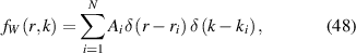
where N is the number of simulation particles and  is the weight, or affinity, attached to each of these particles. Absorbing boundary conditions on the exit boundaries from the device may be instituted in a very easy manner. An important aspect of the affinity is its sign and magnitude change during the simulation. The nonlocal Wigner potential determines the change in the affinity that each particle possesses. That is, the wave nature of the particles is maintained through the variation of each particle's affinity. This affinity was used for figure 3.
The weight and the affinity are really artificial numerical quantities whose purpose is to simulate the quantum phase interference that occurs during real propagation within a semiconductor device. A melding of these two concepts was pursued in another approach [263], which led to the adoption of a pure sign convention [264, 265]. This creates a model in which the Wigner function is considered to include a Boltzmann-like scattering term, and a generation term. The quantum information is carried by the sign of the quasi-particles. This approach is most useful when treating the interaction with the non-local potential as a scattering event. When a scattering event from the potential occurs, two new particles are created, and thus two new wave packets, one with the momentum increased by q and one where it is reduced by q, with q determined randomly from the probability distribution of the potential's spatial Fourier transform. The sign on one of these new particles is taken to be the same as the incident particle, while the sign on the other is the opposite. These signs are taken into account in each averaging process that is used to find average values. Equivalent particles with opposite signs annihilate one another when they meet in phase space, i.e. when their wave packets overlap. This approach was used for figure 12. The Wigner Monte Carlo approach was used to simulate double-gate MOSFETs [266], especially on the nano-scale [267]. In figure 26, the schematic of a nano-scale double-gate MOSFET is shown for these simulations. The source and drain regions are heavily doped and are degenerate, while the channel region is undoped and has a gate length of 6 nm. The Si layer thickness is taken to be 3 nm. In figure 27, the quantum calculation is compared to a classical calculation for the lowest sub-band occupancy in the sub-threshold region. Interference fringes may be seen in the quantum calculation, but not in the classical simulation.
Figure 26. The simulated double-gate MOSFET structure. Highly doped source and drain regions are 15 nm in length. [267] John Wiley & Sons. © 2008 WILEY-VCH Verlag GmbH & Co. KGaA, Weinheim.
Download figure:
Standard image High-resolution image
Figure 27. (a) Cartography of the Wigner function for the lowest subband in the (100) valleys of the Si in the sub-threshold region (VGS = 0.25 V, VDS = 0.7 V) at 77 K. (b) The equivalent distribution for a semi-classical simulation at the same bias and temperature. [267] John Wiley & Sons. © 2008 WILEY-VCH Verlag GmbH & Co. KGaA, Weinheim.
Download figure:
Standard image High-resolution imageThe above simulation for the sub-threshold behavior gives results similar to those for the transistor when it is turned on. In figure 28, the Wigner function is shown for the lowest propagating sub-band in a gate-all-around cylindrical nanowire Si MOSFET with diameter of 50 nm diameter and channel length of 60 nm [268]. It may be seen that the lowest sub-band, which is pictured, moves smoothly through the device, accelerating in momentum as it follows the electric field. Both ballistic transport and scattering due to impurities and acoustic phonons are shown. In either case, as well as the sub-threshold behavior of figure 27, the current-carrying carriers are not relaxed well in the drain. One can clearly see the separation of these carriers from the main body of carriers in the drain in figure 28. Similar behavior has been reported by Croitoru et al [269, 270].

Figure 28. Contour plots for the partial Wigner functions (of the current-carrying lowest mode) and the main body of carriers in the source and drain. The biases are VG = 1 V and VD = 0.3 V. (a) The ballistic case. (b) The case for scattering by impurities and phonons. Reprinted from [268], Copyright (2002), with permission from Elsevier.
Download figure:
Standard image High-resolution imageAs remarked above, many approximations are used to include collision effects and scattering within the Wigner approach. These are typically the normal semi-classical scattering functions, modified slightly to account for off-shell effects and collisional broadening. Levinson has developed a formal approach to Wigner scattering [271], and his results support this approach. In quantum transport, scattering from a phonon, for example, does not have to be local; the event may spread over a small spatial distance. The collision is not instantaneous, but takes a few femtoseconds to be completed [272]. With the intra-collisional field effect, in which the particle continues to be accelerated by the field during this short time, the particle also moves a short distance, which makes it nonlocal. In addition, the loss of a one-to-one correspondence between energy and momentum leads to broadening of the energy conservation that arises from replacement of the delta function by the spectral density function.
While it is not something that is often discussed with the Wigner function, the momentum arises from the difference in the two positions of the wave functions, as may be seen in (44) and (45). The momentum is therefore normal to the main diagonal in the density matrix. The time duration is the time required to transit between the two positions at the corresponding momentum. These different variables are thus tied together in a self-consistent manner. Many methods have been suggested to include the collisional displacement as a modification to the use of semi-classical scattering within the Monte Carlo method [273–275]. To properly include the role of the finite collision duration, we need to account for two effects: (a) the collision duration itself and the resulting energy shift, and (b) the position change during the collision. During the collision, the position changes approximately as [276, 277]
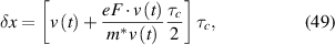
where F is the electric field and  is the collision duration. The first term is just simple displacement due to the particle's motion. The second term represents the intra-collisonal field effect. During the interaction, there is an overlap between the two wave packets at the two positions separated by
  . The two wave functions are Wigner packets which may be taken to be Gaussian in shape, which leads to the probability for a given shift
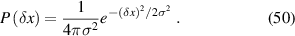
Here, σ is the rms width of the wave packets. The direction of the shift is given by the angle between the velocity and the electric field in the dot product of (49). This provides a method of incorporating the displacement in time and space when using the semi-classical (instantaneous) approximation for the scattering process.
Generally, the collision duration may be considered to be exponentially distributed, and then may be estimated by

where  is the maximum collision duration determined from direct calculations [272] and r is a random number between 0 and 1. In figure 29, the average displacement during the collision is plotted for a simulation of a resonant tunneling diode [277], with the tunneling structure centered around x = 0. The RTD structure contains 3 nm barriers of 0.3 eV height and a 5 nm well. It may be seen that, away from the tunneling region, the rms displacement is about 0.6 nm. But in the tunneling region, the rms displacement can be much larger. This is because the field is considerably larger around the tunneling structure (due to the barriers), where most of the potential drop occurs. Here, the displacement is peaked in the direction of the electric field, and clearly shows the increase due to the intra-collisional field effect.

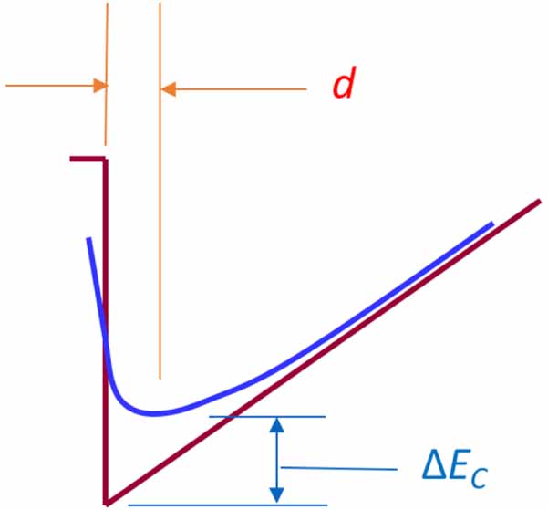
Figure 29. Average (rms) amplitude of the collision displacement during scattering as a function of position in a resonant tunneling diode. The tunneling structure is located at x = 0. The large increase near the tunneling structure arises from the high electric fields in this region. The red curve is for V = 0 across the device, while the blue curve is for V = 0.5 V. Reprinted from [277], Copyright (2003), with permission from Elsevier.
Download figure:
Standard image High-resolution image
4. Discussion
The FET is a simple device in concept. However, in reality, it is a very complex system, and the simulation of it also may be a very complex endeavor, involving full simulation of the processes by which it is created, as well as simulation of its operation and resulting characteristics [278]. This complexity arises not merely from the need for a deeper understanding of the transport of such small or large systems, but also because these devices interact with their environment. From a physical point of view, a device comprises an active region, which is open to the environment in which it is embedded. This connection to the environment may be through a set of contacts, or through interactions with the phonon structure of the lattice upon which the device lies, or through other types of interactions, as mentioned below. The experienced device engineer will recognize that measurements are made in the environment, not within the device, so treatment of the environment is essential. The central feature of these devices is that the device dynamics cannot be treated in isolation and must be considered in conjunction with this environment [31, 53], including the array of other devices and interconnects nearby [279]. This is especially true in the quantum regime [59].
Device–device interactions have not been discussed much recently, but are known to be important in even larger devices than some of those encountered today. It is known, for example, that hot carriers in FETs can emit light [280]. This light emission is believed to arise from intra-conduction band radiative transitions of the hot carriers [281, 282]. These photons have been observed to excite carriers in the substrate which then affect an adjacent device, by modifying the substrate bias [283, 284]. It is also known that clocking an interconnect line can affect charge stored in a nearby potential well [279]. This produces a nonlinear pumping that can excite carriers out of the well, which has consequences for memory devices. So there are a variety of methods whereby a device can interact with neighboring devices and with interconnects, all of which are part of the environment in which a device is situated. These effects can clearly be amplified in quantum controlled devices. At the same time, these interactions have been pursued for the idea of quantum dot array processing [285, 286].
While we have largely examined the entire range of quantum effects that could occur within a FET, it must be pointed out that the FET is not a '...one size fits all...' device. FETs range from the ultra-small to the ultra-large, and they may be digital or analog or mixed-signal devices. They may work at dc or at THz frequencies. In any of these cases, quantization in the inversion/accumulation layer is almost always going to occur, but may never be observable in the device characteristics. It is easy to see that a given device may have little in the way of quantum effects, or it may be a maximum quantum device. We have tried here to cover most of the quantum effects, and the manner in which they may be simulated, but it is up to the device engineers to determine if any or all of these effects are germane to their device.
Transport in these complex FET systems requires a complex quantum description, which takes into account coherent phenomena, as well as dissipative processes of scattering, with both modified by the interaction with the environment as well as by the onset of quantum effects, such as the intra-collisional field effect. There are many approaches to study the quantum effects, as detailed in section 3. Our preference is for the Wigner function, as perhaps was evident in this preceding section. The use of the Wigner function is particularly useful in studies of complex systems, as it may explicitly illustrate the important quantum effects and entanglement that is a signature of quantum interactions. Particle approaches and Monte Carlo simulation of the quantum Wigner function provide an efficient approach to the study of such methods. It becomes clear how to study each process with this approach and to establish its importance in the behavior of the overall system. The Wigner function allows one to clearly identify the quantum effects, particularly the entanglement that arises between different parts of the quantum system.
However, the industry has kind of gone in a different direction, with NEGF becoming increasingly applied in practice. But there are problems with NEGF, both conceptually and with implementation in FETs. These have been discussed in section 3.3, and should not be ignored, if for no other reason than that they call into question the accuracy of present approaches to NEGF. Moreover, the assumption of merely using quantum approaches for the channel region, and coupling to the source and drain 'contacts' by a simple self-energy term ignores a great number of important effects. Not the least of these are the effects illustrated in figures 13, 23, 24, 27 and 28, where the hot carrier energy relaxation has not been completed even 10 s of nm into the drain region. Failure to capture these important effects can lead to simulations that are far removed from reality.
The reader may have observed that most of the discussion concerns the steady-state behavior of the FETs, and not the behavior beyond dc. This is primarily because that studies for the latter are somewhat limited. Nevertheless, the time-dependent behavior has been reviewed [287] in a special issue of the Journal of Computational Electronics on this particular topic. It turns out that any of the various approaches to quantum transport discussed in section 3 can be adapted to study the transient and steady ac response of devices, although some have not been applied to FETs.
The wave function approach of section 3.1 has been used to study microwave oscillations in a mesoscopic ring [288], transport through nanowires in the presence of the spin–orbit interaction [289], ac response of quantum point contacts [290], and the dynamic response of laser structures [291]. Nevertheless, these approaches can be improved, and it should be noted that, to date, no one has addressed the transient response of a simple quantum point contact even though detailed measurements are available [292]. Part of the problem with this approach, as with any approach whether quantum or classical, is that the transient response depends significantly upon the circuit in which any FET is embedded.
The density matrix often appears in the form of a quantum master equation, and this can easily be used to study the ac response of a system [293]. This has been applied to the sub-picosecond response of a mesoscopic system, such as a resonant tunneling diode [294]. This has also been used to look at the initial stages of optical absorption in a semiconductor [295], and this has been applied to the transients in pump-probe spectroscopy [296].
NEGF has been used to study short-time behavior for many years. Transient transport in bulk semiconductors has been studied [297, 298]. A general NEGF approach to open systems has also been discussed [299]. NEGF has also been used to compute the actual collision durations for optical phonons interacting with electrons [272, 300]. More recently, general time-dependent transport has been reviewed [301].
Transient response of resonant tunneling diodes was studied with Wigner functions was first done quite some time ago [302]. More recently, the decoherence behavior of scattering has been studied with the Wigner function [303]. Transient behavior in devices has been studied by the Monte Carlo techniques for decades, so that the Monte Carlo approach to Wigner function modeling is quite easy to use for the transient behavior of FETs as well. This follows on from the general particle trajectory approach [304].
Most of these quantum approaches can be extended to the study of noise as well. Noise can arise from many different sources within a device, and the field needs a full book to treat it in a coherent manner. A brief review of the noise and the two-time correlation functions needed due to the finite bandwidth of a device is given in [287]. A final point is that consideration of most devices at high frequencies usually also involves solutions of Maxwell's equations, often through an approach that couples the electromagnetics to the self-consistent device simulation.
5. Conclusions
In this review, we have tried to present quantum effects in a manner which draws attention to how they will appear in FET characteristics, as well as how they will affect the transport. In addition, we have tried to review the various approaches to quantum transport that have been applied to describe FETs. Of course FETs come in variety of flavors, and one has to evaluate what can occur in any device of interest. The palette presented here is meant to inform these evaluations for the device of interest.
One important aspect is that most of the approaches to quantum transport, including both Wigner functions and the density matrix, require proper initial conditions. While quantum transport remains over the horizon from most FETs today, it may be expected that this will not remain the case in the foreseeable future. We hope that this review has helped to ease the transition to that future.
Acknowledgments
The financial support by the Austrian Science Fund (FWF): P33609, Austrian Federal Ministry for Digital and Economic Affairs, the National Foundation for Research, Technology and Development, and the Christian Doppler Research Association is gratefully acknowledged.
Data availability statement
The data that support the findings of this study are available upon reasonable request from the authors.
Appendix.: Failure of the Keldysh approach
In equilibrium quantum mechanics, use is made of a unitary operator  , in which
  is used as a normalization to the vacuum state,
where  is an appropriate interaction term (or terms) of the Hamiltonian. This means that the interaction is turned on (and off) adiabatically from the infinite past (or infinite future). Keldysh [242] modifies this to move from the infinite past to
  and then return to the infinite past, but retains the assumption that the operator (A1) is unitary. One important point is that the normal trajectory (from past to future) leads to a cancellation of disconnected Feynman diagrams in the equilibrium case [198]. But in real devices, the interaction is neither turned on adiabatically, nor turned off adiabatically, as was pointed out in section 3.3. In reality, quantum field theory (QFT) deals with self-energy corrections, which have imaginary parts. In QFT these lead to divergences, which are sometimes overcome with renormalization of the masses. But imaginary parts of the energy lead to problems with (A1), as it may not result in unitary behavior. Moreover, the expansion of (A1) into a series of terms (from which diagrams may be constructed to evaluate the terms) has never been shown to converge [305]. In the derivations of (30), several of the terms have their own included commutators, and this leads to nested commutators, such as in the current–current correlation functions used to compute the conductivity [198]. In real systems, this can lead to disconnected diagrams and a failure of Wick's theorem [305, 306], and the need for doubled diagrams (such as those used in the Bethe–Salpeter equation [57]). Moreover, some of the terms that arise do not arise from Wick contractions, and the many additional terms lead to the doubled diagrams [307].
As noted, disconnected graphs are assumed to be canceled in equilibrium Green's functions. But, this is not the case in nonequilibrium theory. Disconnected graphs represent two or more interaction processes occurring among separate groups of particles which have physical reality, but are usually omitted from the Dyson equation [308, 309]. Here, these particles have direct particle–particle interactions, and these disconnected graphs lead to phase factors that are important in interference terms. In a modern example, these phase factors are known to be important in the braiding approach to quantum computing [310].
Doubled Feynman graphs, especially the two-particle graphs, appear automatically when particles interact with one another. Even tripled graphs can be necessary, for example when one has to deal with propagators for the nonequilibrium phonons. More importantly, these graphs often signal the need for two-particle Green's functions. In (38), the last terms on the right are actually two terms, due to the matrix product. Each Σ and G involves a creation and an annihilation field operator, which means this product term actually involves two of each operator. The two resulting terms in the matrix product arise from matching one annihilation operator with each of the two creation operators. In fact, the product of these four operators lead to a two-particle Green's function [311]. Even Feynman noted that these two-particle Green's functions are difficult to analyze and approximated them with the pair of one-particle functions [312], as Keldysh has done. But this does not make it correct, and the two-particle Green's function is usually solved using the Bethe–Salpeter self-consistent integral equation [313]. Even simple impurity scattering requires solution of the Bethe–Salpeter equation for the two-particle Green's function to accurately arrive at even the classical result.
Another example of the impact of the two-particle Green's function is in heavily-doped semiconductors, where both the number of electrons and the number of ionized impurities is large. In considering the interactions between these two scattering processes (electron–electron and electron–impurity), does one screen the impurities with the electrons as done classically, or screen the electron–electron interaction with the impurities? If one wants to incorporate the contribution of the electron–election interaction to band-gap narrowing, the latter has to be used [314]. In this case, the interaction site in the Feynman diagram is given a vertex correction, which is composed of the ladder diagrams arising from the normal two-particle Green's function evaluation of the Bethe–Salpeter equation for impurity scattering, but with the two Feynman lines pulled together at one end [55].
From these considerations, it is apparent that using NEGF based upon the Keldysh approach is a somewhat simplistic approach to quantum transport in real devices. Use of the adiabatic approximation for paths and the avoidance of two-particle Green's functions are serious deficiencies. Even the avoidance of disconnected graphs can lead to large errors in interference cases such as those illustrated in figures 12 and 13.
Footnotes
- 4
Lilienfeld's patent was filed in 1926.