

Abstract
Niobium thin films are used at CERN (European Organization for Nuclear Research) for coatings of superconducting radio-frequency (SRF) accelerating cavities. Numerical simulations can help to better understand the physical processes involved in such coatings and provide predictions of thin film properties. In this article, particle-in-cell Monte Carlo 3D plasma simulations are validated against experimental data in a coaxial cylindrical system allowing both DC diode and DC magnetron operation. A proper choice of ion induced secondary electron emission parameters enables to match experimental and simulated discharge currents and voltages, with argon as the process gas and niobium as the target element. Langmuir probe measurements are presented to further support simulation results. The choice of argon gas with a niobium target is driven by CERN applications, but the methodology described in this paper is applicable to other discharge gases and target elements.Validation of plasma simulations is the first step towards developing an accurate methodology for predicting thin film coatings characteristics in complex objects such as SRF cavities.
Export citation and abstract BibTeX RIS

Original content from this work may be used under the terms of the Creative Commons Attribution 4.0 licence. Any further distribution of this work must maintain attribution to the author(s) and the title of the work, journal citation and DOI.
1. Introduction
Thin film coatings used at CERN (European Organization for Nuclear Research) cover a wide range of applications including non-evaporable getters for distributed pumping [1] and amorphous carbon for electron cloud mitigation [2]. We focus here on niobium on copper (Nb/Cu) thin film deposition used in the production of superconducting radio-frequency (SRF) accelerating cavities, as an alternative to bulk niobium cavities [3].
The Nb/Cu technology has been developed and studied at CERN since the large electron positron collider era [4]. State-of-the-art production of superconducting niobium coatings in RF cavities involves either DC diode or DC magnetron sputtering configurations with external solenoidal field or permanent magnet assemblies [3]. The wide variety of shapes and sizes of SRF cavities usually implies an expensive and time-consuming experimental optimisation phase to design the coating system suited for each specific geometry [5]. The link between thin film properties and RF performances of the coated cavity is non-trivial [6]. The use of numerical simulations could help in the design of sputtering sources and tuning of the deposition process, providing qualitative (relative thickness uniformity) and quantitative properties (absolute thickness profile, film morphology).
In this article, we focus on the numerical simulation of the DC discharge itself with the validation of two physical parameters which have a strong impact on the plasma behaviour: the secondary electron emission yield induced by argon ion bombardment on the niobium target, and the initial energy distribution function of the secondary emitted electrons from the niobium cathode. Validating these two parameters is essential since the plasma distribution along with discharge voltage and current are responsible for the target erosion profile, which in turn plays a large role in the coating properties. The influence of ion induced secondary electron emission (IISEE) parameters has been demonstrated in radio-frequency discharges between parallel plates with one-dimensional in space simulation codes. For example, in [7], the transition between 'wave-riding' and 'secondary electron' regimes is attributed to the secondary electrons emitted from the electrodes under ion bombardment. In [8], an asymmetric plasma response is noticed when electrodes of similar areas possess different secondary electron yields, which is used in [9, 10] to attempt a separate control of ion mean energy and ion flux at the electrodes in dual-frequency capacitive discharges. At last, the dependence of the secondary electron yield on the bombarding ion energy is discussed in [11, 12] for argon discharges and [13] for oxygen discharges by assuming 'non-clean' electrode surfaces. In the present study focussed on DC discharges, constant sputtering of the cathode under ion bombardment ensures stable discharge voltages after cathode conditioning (removal of adsorbed impurities and oxide layer). This leads us to neglect the contribution of ion energy-dependent so-called kinetic emission to the total secondary electron emission. Therefore, for clean metal surfaces, we only consider potential emission which predominates at ion energies below a keV [14] and does not depend on bombarding ion energy.
Reliable data for ion-induced secondary electron yield and energy distribution are often difficult to find for ion energies typically in the range below one keV. Empirical formulas are reported in the literature [15–18], providing yield values between 0.12 and 0.16 for potential emission of electrons by argon ions on niobium.
To validate the simulation results, we developed a dedicated experimental system which can be operated both in DC diode and magnetron configurations with the addition of an external solenoidal magnetic field, similarly to the HIE-ISOLDE cavity coating apparatus [19]. In the diode configuration, the initial energy distribution of the electrons (a few eV) does not require precise modelling since electrons are radially accelerated away from the cathode by the electric field in the cathode sheath to several hundreds eV. In the magnetron case, their initial energy distribution plays an important role since the magnetic field can induce electron recollection on the cathode surface [15, 20]. Therefore, a suitable ion-induced secondary electron emission yield γIISEE value is numerically assessed as a first step in diode by assuming a uniform initial electron energy distribution in the [0–5] eV interval. Then for the magnetron case, the approach described in [21] is followed, by approximating the energy distribution of the secondary electrons as a Gaussian centred on  with a cut-off energy at Ei − 2ϕ, where Ei is the argon first ionisation energy (15.76 eV), and ϕ is the niobium metal work function (4.2 eV).
The paper is organised as follows: we first describe the experimental system along with the numerical parameters used in the particle-in-cell Monte Carlo (PICMC) simulation code. Secondly, experimental and simulated discharge voltages and currents are presented in diode and magnetron at different pressures, including comparison of electron density, energy and electric potential profiles obtained from simulations and from Langmuir probe measurements.
2. Materials and methods
2.1. Experimental setup description
The experimental system (figure 1) designed to validate the simulation results consists of a 1.1 m vertical vacuum chamber of 200 mm inner diameter. Pumping is ensured by a turbomolecular pump (60 l/s pumping speed for N2) backed up by a primary pump. The system base pressure is in the 10−7–10−6 mbar range in the main chamber without bake-out. Argon is injected in the main chamber through a variable leak valve, and two capacitive diaphragm gauges are located at the top and bottom of the chamber in order to precisely control the argon process pressure in the chamber during the plasma discharge. A coil made of 2.8 mm diameter insulated copper cable and wound around the main chamber provides a solenoidal axial magnetic field described in section 2.4. This solenoid has an inner diameter of 220 mm, and a total height of 990 mm.

Figure 1. (a) Schematic cutview and (b) picture of the experimental setup. The grounded stainless steel anode is attached to the top flange using fixation threads, and the discharge power is applied on the niobium cathode. The whole assembly is inserted in the vertical vacuum chamber with an external solenoid winding.
Download figure:
Standard image High-resolution imageA niobium rod cathode (18 mm diameter, 303 mm length) is coaxially mounted inside a stainless steel anode (125 mm average diameter, 500 mm length) as shown in figure 1. The anode is made of two half shells creating an octagon, such that diagnostics (quartz balance, sample for thickness analysis not used in this study) can be easily mounted on the planar faces while keeping the azimuthal symmetry close to that of a cylinder. The cathode–anode distance of 51.5 mm is chosen equal to the one between substrate and cathode in the HIE-ISOLDE coating assembly [22]. The anode is grounded through fixation threads attached to the main chamber top flange, and a negative bias voltage is applied on the cathode by an MDX 500 advanced energy power supply unit. This unit can deliver up to 1000 V–0.5 A with an accuracy of 0.2% of the full rated output, and is used to apply and read discharge voltage and current values. It is operated in power regulation mode.
2.2. Langmuir probe analysis
A Langmuir probe is mounted on a linear motion vacuum feedthrough of 405 mm stroke length. This allows measurements of axially resolved plasma density, electron temperature and plasma potential to compare with simulation results. The probe consists of a 1 mm diameter tungsten wire (rprobe = 0.5 mm) inserted in a 1.6 mm inner diameter, 3 mm outer diameter alumina tube attached to a vertical rod outside of the anode and connected to a vacuum-compatible coaxial cable insulated with kapton, as seen in figures 1 and 2. The effective tungsten tip length Lprobe immersed in the plasma is of 2 mm, and the middle of the tip is located at 27 mm from the cathode axis with an uncertainty of ±1.5 mm due to the geometrical design. A slit in the anode allows vertical motion of the probe.

Figure 2. Schematics of the Langmuir probe assembly. Zoomed view from figure 1(a). The white dashed line represents the vertical axis of the cylindrical vacuum chamber.
Download figure:
Standard image High-resolution imageTo obtain values of plasma parameters comparable to the simulated ones, the probe is operated in sweeping mode by applying a triangular voltage Va varying between −40 V and +3 V at a sweeping frequency f = 13.1 Hz. The current drawn by the probe is recorded by a Lecroy HDO6104 oscilloscope. Current density/voltage (J/Va) characteristics are analysed according to the procedure suggested in [23, appendix B.4]. First, the plasma potential V0 [V] is estimated as the voltage corresponding to the maximum of the J/Va characteristics first derivative. Then, the electron temperature Te [eV] is estimated as  4
where J0 [A m−2] and k0 [A m−2 V−1] are, respectively, the current density and the slope of the I/V characteristics at the plasma potential. The plasma density n0 [m−3] is estimated as
4
where J0 [A m−2] and k0 [A m−2 V−1] are, respectively, the current density and the slope of the I/V characteristics at the plasma potential. The plasma density n0 [m−3] is estimated as  where e is the base of the natural logarithm, and Vf [V] is the floating potential. These four values are taken as initial guesses in a four-parameter fit of the J/Va characteristic from Vf to V0, with the approximated expression of the current density collected by a cylindrical probe Japprox(Va) [A m−2] given by Guittienne et al [23] in equation (B12):

This fit provides final values for Te, V0, n0 and Vf, with experimental error bars taking into account probe area uncertainty and error estimates on the determination of initial V0, n0 and Ee (converted from Te by assuming a Maxwellian electron energy distribution) before the final four-parameter fit. At last, we estimate that the methodology used here to analyse (J/Va) characteristics is associated with an error margin of ∼20% in the pressure range of interest.
2.3. Particle-in-cell plasma simulations
Plasma simulations are performed on a high performance computing cluster installed at CERN with a PICMC parallel code developed at the Fraunhofer IST [24–26]. The simulation geometry includes cathode, anode, insulating ceramic and surrounding vacuum chamber. Surface meshing and physical surfaces definition are obtained with the open source software Gmsh [27], which is also used for visualising simulation results. Anode and chamber are defined as grounded elements, insulating ceramic as floating, and the negative bias voltage on the cathode is adjusted throughout the simulation run by a feedback loop enforcing the power setpoint.
A summary of the numerical and physical parameters is presented in table 1. To compare simulation results with experiments, a power setpoint Pdis of 20 W is applied for all cases. Higher powers would result in higher currents and plasma densities, and unfulfillable numerical constraints in terms of time step and mesh size due to computational costs. The Cartesian simulation volume mesh is refined inside the anode where the plasma is denser, and made coarser outside of it. To ensure proper collision statistics, the scaling factor representing the number of argon simulation particles with respect to real particles is adjusted for each pressure to have about ten argon numerical particles in each 1 mm3 cell inside the anode. Volume reactions used in the simulation model involving argon atoms, ions, and electrons were described in [26], while surface reactions assume that electrons and argon ions impinging on surfaces are collected there, with the emission of one neutral argon atom and a number of electrons according to the value of γIISEE for each collected ion. Electrons impinging on a physical surface are collected with a probability of 1 without further re-emission. Secondary electron emission under neutral, metastable or photon bombardment is also neglected.
Table 1. Physical and numerical simulation parameters.
| Domain size [mm3] | 210 × 210 × 1100 |
| Mesh size inside the anode [mm3] | 1 × 1 × 1 |
| Species | Ar, Ar+, e− |
| Discharge power Pdis [W] | 20 |
| Time step [s] | 5 × 10⁻¹² |
| CPU used per run (cores) | 112 |
| Scaling factor for Ar+ | 1 × 10⁵ |
| Scaling factor for e− | 1 × 10⁵ |
| Simulation time | Several weeks/months |
| Diode | Magnetron | |
|---|---|---|
| Peak magnetic field [Gauss] | 0 | 160 |
| Ar pressure pAr [mbar] | 0.2, 0.3, 0.4 | [3, 5, 7, 9]× 10−2 |
| γIISEE | Varied | 0.13 |
| IISE energy distribution | Uniform in [0–5] eV | Gaussian |
| IISE angle distribution | Cosine | Cosine |
| Electron capture probability | 1 | 1 |
The choice of these numerical parameters could lead to some inaccuracies in the simulation results presented in this manuscript. First, the mesh size of 1 mm is not resolving the Debye length for the typical densities and energies simulated here. This could induce so-called numerical heating [28], meaning that insufficient spatial resolution of the electric field could result in artificially too high electron kinetic energies. However, a finer mesh size would make simulation runs even longer and practically impossible to carry. To partly mitigate this issue, the stability of each simulation in terms of cathode voltage convergence, sufficient cathode sheath resolution and absence of abnormally high electron energies in the plasma volume are ensured. Then, absence of secondary electron emission due to sources other than ion bombardment and uncertainties inherent to the collision cross-sections model could also alter the presented results. The impact of these choices on the simulation inaccuracies and in particular on the assessed IISEE parameters is quite challenging to quantify and is beyond the scope of the present study. Discussions on this matter can be found in [10, 12, 13] in the case of radio-frequency discharges simulated with one-dimensional in space codes.
2.4. Magnetic field
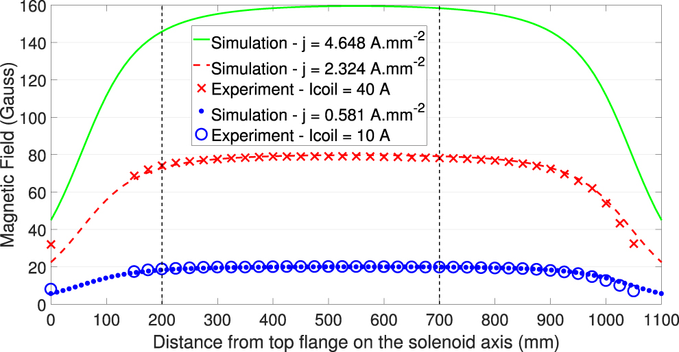
Magnetron simulations require a magnetic field map as an input to the plasma simulation code. This map can either be computed by the boundary element method module of the PICMC code in the case of permanent magnet assemblies, or imported as a 3D text file from an external source. In the present case, we choose the latter option and compute the magnetic field generated by the solenoid using the magnetostatic module of the Opera commercial simulation software [29]. Figure 3 shows the good agreement between the simulated axial component of the magnetic field and the corresponding quantity measured on the solenoid axis with a gaussmeter for different coil currents. The simulated axial component of the magnetic field corresponding to a simulation current density of j = 0.581 A mm−2 is found to match the experimental value generated by a current Icoil = 10 A, as shown by the blue curves in figure 3. A linear scaling of the simulation current density and of the experimental Icoil at, respectively, j = 2.324 A mm−2 and Icoil = 40 A shows a consistent agreement between simulation and measurement (red curves of figure 3). Therefore, the simulated field generated with j = 4.648 A mm−2 (whose axial component is plotted with a green straight line in figure 3) is selected for the magnetron simulations which will be presented in section 3.2 as an accurate 3D representation of the experimental field generated with a current Icoil = 80 A (not measured). The axial positioning of the anode at 200–700 mm below the main chamber top flange is chosen such that the anode lies in the uniform field region (B ∼ 160 Gauss, see figure 3), thus minimising edge effects on the plasma due to non-uniformity of the magnetic field.

Figure 3. Comparison of the axial component of the solenoidal magnetic field computed with the Opera software [29] and its value experimentally measured at different solenoid currents on the solenoid axis. Black vertical dashed lines at 200 mm and 700 mm identify the octagonal anode top and bottom locations, respectively.
Download figure:
Standard image High-resolution image3. Results and discussion
3.1. Numerical assessment of γIISEE in the diode configuration
In this section, a suitable value of γIISEE is numerically assessed in the diode configuration by comparing global discharge currents and voltages between simulations and experiments as a function of the argon gas pressure.
Three simulations are performed in the DC diode configuration for different γIISEE with pAr = 0.3 mbar. As can be seen in table 2, increasing γIISEE leads to a discharge voltage decrease (respectively a current increase) since it entails more electrons emitted from the cathode towards the plasma region. Moreover, a simulation yield of 0.13 fits the experimental current and voltage values for this given pressure within the experimental uncertainties.
Table 2. Comparison of simulated voltages and currents at different secondary electron yields γIISEE with experimental values in diode for pAr = 0.3 mbar, Pdis = 20 W.
| Voltage [V] | Current [mA] | ||
|---|---|---|---|
| Experiment | 400 | 51 | |
| Simulation | γIISEE | ||
| 0.10 | 454 | 44 | |
| 0.12 | 418 | 48 | |
| 0.13 | 399 | 50 |
aValues correspond to stable ones after some minutes of operation and removal of the cathode oxide layer. bValues are given for stable simulation currents and voltages at tsim = 7.5 μs.
Then, we perform a parameter scan in process pressure pAr while keeping γIISEE = 0.13. In diode coating processes such as the one of the HIE-ISOLDE cavity [22], a pressure increase leads to a large number of scattering collisions between sputtered niobium and argon atoms and hence high niobium redeposition on the cathode and very low deposition rates [30]. Even though we do not consider sputtering processes in the present study, we choose to vary pAr between 0.2 and 0.4 mbar to be relevant with typical diode process pressures.
It is shown in table 3 that the simulation I/V trend and absolute values match the experimental data. Validity of the IISEEY value is further confirmed by a loss of plasma sustainability for both simulation and experiment at pAr = 0.05 mbar, with voltages saturating at 1000 V and weak currents of, respectively, 1.2 mA and 2 mA being delivered, both failing to reach the 20 W power setpoint.
Table 3. Comparison of experimental and simulated voltages and currents in diode at different pressures for γIISEE = 0.13, Pdis = 20 W.
| Voltage [V] | Current [mA] | |||
|---|---|---|---|---|
| Pressure [mbar] | Measurement | Simulation | Measurement | Simulation |
| 0.2 | 557.9 ± 25.4 | 562.2 ± 0.2 | 37.3 ± 1.5 | 35.6 ± 0.03 |
| 0.3 | 400.4 ± 7.7 | 399.3 ± 0.6 | 51 ± 1.3 | 50 ± 0.2 |
| 0.4 | 339.9 ± 6.7 | 335.5 ± 0.4 | 60.1 ± 1.6 | 59.5 ± 0.2 |
aError is ± the standard deviation σ over 7 different measurements. bError is ±σ over 0.5 μs at 10 μs converged simulation time.
Physical parameters can be extracted from each simulation case, such as electron and ion densities, electric potential and species energies. A map of the electron density distribution is displayed in figure 4(a) for pAr = 0.3 mbar, along with a photograph (visible light spectrum) of the experimental diode plasma taken through a viewport located below the vacuum chamber (figure 4(b)). Figure 5 presents radial and axial plots of the electron density and energy, and radial plot of the electric potential for the three pressure cases. Radial plots represent azimuthally averaged values in the horizontal mid-plane of the cathode, in the discharge gap (9–60.5 mm). Axial plots are similarly obtained from azimuthally averaged values over a 27 mm ± 1 mm radius cylinder around cathode axis, with its axis origin at mid height of the cathode. Displayed electron energies correspond to mean electron energies within each cell.

Figure 4. (a) Electron density [m−3] displayed in the vertical and horizontal midplanes at pAr = 0.3 mbar, diode, γIISEE = 0.13, tsim = 10 μs, Pdis = 20 W. (b) Picture of the diode argon plasma taken from a viewport below the chamber. The apparent plasma displacement is not due to the Langmuir probe, but rather to a slight misalignment between camera and chamber axes.
Download figure:
Standard image High-resolution image
Figure 5. Diode—simulation results for the three process pressures at Pdis = 20 W: radial profiles at tsim = 10 μs of (a) electron density [m−3] and (b) electron energy [eV] in logarithmic scale in the horizontal plane passing through the cathode centre; axial profiles of (c) electron density [m−3] and (d) electron energy [eV] at 27 mm radius (e) radial profile of the electric potential [V] in the horizontal plane passing through the cathode centre.
Download figure:
Standard image High-resolution imageIncreasing the pressure leads to a radial confinement of the plasma as shown by the radial density peak position shift (figure 5(a)), along with a cathode sheath width reduction (figure 5(e)). Indeed, a higher pressure means that electrons accelerated through the cathode sheath experience more collisions with neutral argon particles, hence losing their energy closer to the cathode (figure 5(b)). As seen in figure 5(c), the axial electron density profiles are almost flat around the cathode and quickly drop at the cathode edges (±151.5 mm). This confinement can be explained by two reasons. First, in the absence of a magnetic field, the plasma is electrically driven. Due to the aspect ratio between cathode length (303 mm) and anode average diameter (120 mm), the electric field is almost constant and radially directed, which ensures the axial plasma uniformity around the cathode. Second, the relatively high process pressures limit the axial drift of charged species because of collisions, thus leading to the abrupt electron density axial drops at the cathode edges.
Langmuir probe measurements are performed at the three pressures along the vertical direction, according to the probe configuration described in section 2.2. The probe surface used to convert the probe current into current density is the geometrical area of the probe tip Ap
=  , where rprobe = 0.5 mm and Lprobe = 2 mm. Similarly to the simulation results of figure 5, experimental plasma parameters taken at 27 mm radius from the cathode axis are almost pressure independent in the studied pressure range. Therefore, we only present in figure 6 the comparison of simulated and experimental plasma density, electron energy and plasma potential at pAr = 0.3 mbar. We use a synthetic diagnostic to compare simulations and experiments, where simulated values are extracted from a cylinder of radius 27 mm ± 2.5 mm such that they match the probe spatial resolution. As such, averaged simulated results are presented with error bars corresponding to ±3 standard deviations over the 5 mm radius averaging. Analysis of the J/Va probe characteristics yields the electron temperature Te [eV], which is converted into electron energy Ee [eV] for comparison with the simulated profile of figure 6(b). This conversion assumes a Maxwellian energy distribution for the electrons, i.e. Ee [eV] =
  [eV].
[eV].

Figure 6. Diode—comparison at pAr = 0.3 mbar, Pdis = 20 W of simulation and Langmuir probe profiles of (a) axial electron density ne [m−3] (b) axial electron energy Ee [eV] (c) axial plasma potential V0 [V].
Download figure:
Standard image High-resolution imageFigure 6 shows that experimental electron density (electron energy and plasma potential, respectively) is about twice (respectively about half) of its simulated equivalent in the central axial region (z ∈ [−150; 150] mm). The discrepancy between simulation and experiment could be partly explained by plasma perturbations induced when the probe voltage Va is positively swept above the floating potential Vf. Indeed, electron peak currents collected by the probe are of ∼6 mA, compared to a global discharge current of ∼51 mA (see table 3 for pAr = 0.3 mbar). This could mean that for positive probe voltages Va, electrons are collected from a plasma region beyond the probe vicinity. For a given positive voltage Va above Vf, the electron current is therefore overestimated. This results in an overestimate of the plasma density ne along with an underestimate of the plasma potential V0 and electron temperature Te. This could also explain why the plasma density decay observed in the simulation profile for z < −150 mm and z > 150 mm is not well reproduced in the measurements, since the probe collects electrons from a large plasma region independently of its position. Real plasma parameters without probe perturbation should be closer to the simulated ones. It is also worth mentioning that the probe perturbation does not impact the values given in table 3, since those are taken when the probe is electrically floating and axially positioned at the anode extremity.
3.2. Validation of the secondary electron energy distribution function in magnetron configuration
Electron trajectories are modified in the presence of a magnetic field. In particular and contrarily to the diode configuration, secondary electrons emitted from the cathode surface can be recollected depending on their initial energy distribution, which therefore plays a role in the global I/V discharge parameters. To validate the use of a Gaussian energy distribution of secondary electrons emitted from the cathode, magnetron simulations are run at different pressures with γIISEE = 0.13 according to the results of the previous section 3.1. The magnetic field profile used as input for the simulations was described in section 2.4, corresponding to an experimental axial field of 160 Gauss peak value. Four pressures are chosen, as given in table 1, as a trade-off between minimum pressure needed to sustain the plasma discharge and process-limited higher pressure (same criteria as for the diode study). The other physical and numerical parameters are unchanged.
Table 4 shows the experimental and simulated discharge currents and voltages for the four different pressures. The simulation trend matches the increase of current with pressure and corresponding decrease of voltage. Discrepancies of ∼25–35 V (∼10% of the discharge voltage) can be noticed between measurement and simulation for the same pressure. This could be partly attributed to longer simulation stabilization times in the magnetron configuration with respect to the diode case. Indeed, voltage convergence exhibits an exponential decay behaviour in time such that simulation values given at 30 μs are slightly overestimating voltages and thus underestimating currents. This slow convergence of the magnetron cases could be explained by the drift of the charged species outside of the cathode–anode region. This can be seen in figure 7(a) showing electron density losses at the anode ends, which lead to a larger effective plasma volume and longer computation times as well as longer physical time needed to reach a steady-state. This phenomenon of electron end-losses was described in [31] for such a configuration, and is usually avoided in coating systems such as planar or post-magnetrons. As a trade-off between reasonable computational time and required physical accuracy, the achieved agreement between simulated and experimental values meets the precision required for our practical purpose.
Table 4. Comparison of experimental and simulated voltages and currents in magnetron at different pressures, 160 Gauss peak value, Pdis = 20 W.
| Voltage [V] | Current [mA] | |||
|---|---|---|---|---|
| Pressure [mbar] | Measurement | Simulation | Measurement | Simulation |
| 0.03 | 292.6 ± 3.4 | 326.4 ± 0.1 | 69.3 ± 1 | 61.3 ± 0.1 |
| 0.05 | 267.6 ± 1.6 | 294.3 ± 0.3 | 76.4 ± 1 | 68 ± 0.1 |
| 0.07 | 253.3 ± 2 | 281.2 ± 0.2 | 80.6 ± 1.1 | 71.2 ± 0.1 |
| 0.09 | 243.7 ± 2.7 | 273.5 ± 0.4 | 83.6 ± 1.5 | 73.2 ± 0.2 |
aError is ±σ over 7 different measurements. bError is ±σ over 0.5 μs at 30 μs simulation time.

Figure 7. (a) Electron density [m−3] displayed in the vertical and horizontal cutplanes at pAr = 0.05 mbar, magnetron, γIISEE = 0.13, Gaussian electron energy distribution, tsim = 30 μs. The direction of the axial magnetic field B generated by the solenoid is illustrated by the red arrow. (b) Picture of the magnetron argon plasma taken from a viewport at the bottom of the chamber.
Download figure:
Standard image High-resolution imageFigure 8 presents the electron density and energy radial and axial profiles, and electric potential radial profile for the four pressure cases. Pressure-dependent variations of plotted quantities are less pronounced than for the diode cases (figure 5). The decay of plasma characteristics (ne, Te) is smoother along the z-axis because of electron end-losses bringing the plasma outside of the axial cathode region. Electron energies are about twice higher than in the diode configuration due to lower working pressures. The apparent saturation of the electron density axial profile when the pressure is increased (figure 8(c)) is attributed to a mitigation of the magnetic field influence when more collisions between charged particles and process gas atoms occur, thus limiting the transport of charged particles and tending towards the diode case.

Figure 8. Simulation results in magnetron configuration for the four process pressures at Pdis = 20 W: radial profiles at tsim = 30 μs of (a) electron density [m−3] and (b) electron energy [eV] in logarithmic scale in the horizontal plane passing through the cathode centre; axial profiles of (c) electron density [m−3] and (d) electron energy [eV] at 27 mm radius (e) radial profile of the electric potential [V] in the horizontal plane passing through the cathode centre.
Download figure:
Standard image High-resolution imageLangmuir probe measurements are taken at the four pressures in the vertical axis direction, similarly to the ones described in section 3.1. For the magnetron discharge, the probe surface used to convert the probe current into current density is taken as the projection of the probe tip geometrical surface onto the plane perpendicular to the magnetic field [32]: Ap = 2rprobe Lprobe. Indeed, with B = 160 Gauss and Ee ∼ 2 eV according to simulated values of figure 8(d), the electron gyroradius rL ∼ 0.3 mm is smaller than the probe typical size. Experimental plasma parameters taken at 27 mm radius from the cathode axis are almost identical for pAr ∈ [0.05; 0.07; 0.09] mbar. As such, we only compare experimental measurements with simulated parameters using the synthetic diagnostic described in section 3.1 for the two extreme pressures pAr = 0.03 mbar and 0.09 mbar, as shown in figure 9. Due to the influence of the magnetic field, a non-uniformity of the azimuthal plasma densities, as seen in figure 7(a), is leading to local fluctuations of the azimuthal electric potential profiles. Because of the very different time scales between simulations and Langmuir probe measurements, comparison of azimuthal electric potential profiles cannot be made, as opposed to what was showed in the diode case in figure 6(c).

Figure 9. Magnetron, Pdis = 20 W—comparison of simulation and Langmuir probe profiles at pAr = 0.03 mbar and pAr = 0.09 mbar in semi-logarithmic scale of (a) axial electron density ne [m−3] (b) axial electron energy Ee [eV].
Download figure:
Standard image High-resolution imageFigure 9(a) shows that simulated and experimental electron density profiles agree in shape except for z < −100 mm. The experimental increase in density for these axial positions is consistently measured for all pressures, but remains unexplained. The simulated densities in the central axial region are 6.5 and 3.5 times higher than the experimental ones, respectively, for pAr = 0.03 mbar and pAr = 0.09 mbar, but the trend with pressure matches: a larger pressure results in a larger electron density in both simulation and experiment. Figure 9(b) also reveals an agreement of relative electron energy profiles between simulation and experiment with a matching trend as a function of pressure. However, simulated electron energies are 2.6 to 1.8 times lower than their experimental counterparts, respectively, for pAr = 0.03 mbar and pAr = 0.09 mbar. The currents drawn by the probe are ten to twenty times smaller than the ones in diode and the plasma is therefore not disturbed in the vicinity of the probe. This could explain the reasonable agreement of measurements with simulations in magnetron despite the fact that the theory used for the analysis of Langmuir probe characteristics J/Va does not account for the presence of the magnetic field.
4. Conclusions
A PICMC plasma simulation code was used to model DC diode and magnetron discharges in a full 3D coaxial cylindrical cathode and anode configuration. A yield γIISEE of 0.13 and a Gaussian energy distribution function for secondary electrons emitted under argon ions bombardment on a niobium target were demonstrated to fit experimental discharge currents and voltages for different working pressures. Plasma density, electron energy and plasma potential axial profiles obtained in the simulations were in qualitative agreement with Langmuir probe measurements, and possible reasons for discrepancies in absolute values were provided.
The self-consistent PICMC simulation approach has the advantage of overcoming the use of an 'effective' secondary electron yield to describe the discharge in the presence of a magnetic field (as developed in [15]), since appropriate electrons angle and energy distributions induce accurate modelling of electron recollection on the cathode. Nonetheless, the present study could be complemented by including secondary electron emission under electron, photon or fast neutral bombardment in the simulations, provided that reliable experimental data could be gathered.
A change of gas or target material would require a similar validation process, inducing a possible additional need for the validation of volume collision cross-sections involving other gases than the well characterized argon.
Obtaining the sputtering profile on the target is required for neutral particle transport simulations and prediction of deposition profiles on real SRF cavity geometries. This extension of the presented work will be described in a future article.
Acknowledgments
The authors wish to acknowledge the help of the simulation group from the Fraunhofer IST for discussions and code upgrades, and the support of the Swiss Plasma Centre for providing Langmuir probe electronics and expertise.
Footnotes
- 4
This stems from neglecting the ion thermal velocity
 with respect to the electron thermal velocity , where q [C] is the elementary charge, Ti [eV] is the ion temperature, mi [kg] and me [kg] are the ion and electron masses, respectively.

