

Abstract
To enhance the performance of transition metal chalcogenide composite electrode material, a key point is a composite design and preparation based on the synergistic effect between the oxide and selenide materials. With a facile 'one step template-annealing' step, Ni3Se4, Ni0.6Zn0.4O and ZnO are simultaneously synthesized, by 500 °C annealing. With the increase of annealing temperature from 350 °C to 600 °C, nickel selenides change from NiSe2 to Ni3Se4 to NiSe. The charge storage capacity increases first and then decreases with the increase of annealing temperature, and the 500 °C annealing obtained three compound composite Ni3Se4/Ni0.6Zn0.4O/ZnO (NNZ-500) nanoparticle material displayed a high specific capacitance of 1089.2 F g−1 at 1 A g−1, and excellent cycle stability of 99.8% capacitance retention after 2000 cycles at 5 A g−1. Moreover, an asymmetric supercapacitor was assembled with NNZ-500 as the positive electrode material and activated carbon as the negative electrode material. This kind of asymmetric supercapacitor demonstrated a high energy density of 53.4 Wh kg−1 at 819.0 W kg−1, and cycle stability with 98.6% capacitance retention after 2000 cycles. This material preparation approach provides great potential for the future development of high performance transition metal composite electrode materials in energy storage applications.
Export citation and abstract BibTeX RIS
1. Introduction text
At present, electrochemical energy storage devices, especially supercapacitors (SCs) have attracted huge interest due to their high power density, long cycling lifetime, fast charge and discharge rates, and environmental friendliness [1–4]. Electrical double layer capacitors (EDLCs) and pseudocapacitors are the two most typical types of SCs, based on their charge storage mechanisms [5, 6]. EDLCs employ carbon materials (activated carbon, graphene, carbon nanotubes and so forth), utilizing their high surface area, which store charges accumulated at the electrode/electrolyte interface [7]. Using transition metal compounds (such as RuO2, NiO, MnO2, etc), pseudocapacitors typically rely on the fast and reversible redox reactions near the active material surface to store charges [8–10]. Pseudocapacitor materials can have higher specific capacitance than materials of EDLCs [11] but the energy densities of the pseudocapacitor materials are still far lower than that of the advanced battery materials [8].
Nowadays, asymmetric supercapacitors (ASCs) are effective energy storage device to increase the energy density, as compared to pure EDLC devices [12]. In ASCs, people use pseudocapacitor-type in the positive electrode to achieve high energy density, and EDLC-type material in the negative electrode to achieve high power density [7, 13, 14]. Transition metal chalcogenide compounds, such as oxides and sulfides have been extensively studied for positive electrode applications because of their abundant redox active sites, excellent electrical conductivity and good rate capability. However, the low-rate capability of metal oxides and the poor cycling stability of metal sulfides can reduce their electrochemical performances [15, 16]. Zhang et al [17] reported directly synthesis the Co3O4 nanowire on nickel foam, and delivered a specific capacitance of 1160 F g−1 at 2 A g−1, and 820 F g−1 at 20 A g−1. However, there is the drawback of the low weight fraction of the active material in the electrode, which will sacrifice the energy density of the full device. Zhu et al [18] used a template-engaged conversion method to synthesize hierarchical NiS hollow spheres. Despite the relatively high capacitance of 927 F g−1 at 4.08 A g−1, the metal sulfides have poor cycling properties. Se element also belongs to the VIA group as O and S, while the chalcogenide compounds of transition metal selenides, such as nickel selenides, are expected to have higher electrical conductivities than the corresponding oxides and sulfides, and can play important roles in electrochemistry, with high electrochemical reaction rates and capacitance [19–21]. Compared with single nickel selenide, multi-component nanocomposites can make full use of the synergistic and complementary effects among the different components, which gives them greater advantages in application [22–24]. Chebrolu et al [21] successfully synthesized a multicomponent electrode with NiCu(OH)2 wrapped Ni–Cu–Se co-axial nanoparticle structure via the co-electrodeposition technique, which showed a specific capacitance of 264.9 F g−1 at 1 A g−1 and 75.7% retention after 3000 cycles. Due to the contribution of the synergistic effect, where Ni–Cu–Se provides high specific capacitance and high conductivity, and NiCu(OH)2 provides the main support for the structure, the composite material performance remains stable after 3000 cycles. A few papers have been further devoted to investigating the synergistic effects of nickel selenide complexed with transition metal oxides. Wang et al [22] reported hydrothermally synthesized NiMoO4/NiSe2/MoSe2 nanowires, which deliver a relatively high capacitance of 955 F g−1 at 1 A g−1, and 86.1% capacitance retention after 5000 cycles at 10 A g−1. Compared to NiMoO4, the electrochemical performance of NiMoO4/NiSe2/MoSe2 is improved in all respects, due to the oxides and selenide contribute individually to rich redox reactions and remarkably increased electrical conductivity. However, this synthesis method is relatively cumbersome, where NiMoO4 was firstly hydrothermally synthesized, and was then partially converted to NiSe2 and MoSe2 through in situ selenylation of the NiMoO4 with Se powder. Moreover, it is also difficult to control the morphology and size of the nanoparticles. It is important to synthesize composites with multiple components through facile preparation steps, to maximize the synergistic effects for material performance improvement, and to reduce the material preparation costs. However, to the best of our knowledge, one-step annealing preparation of three-phase composites of oxide and selenide compounds has not been reported.
In this work, we synthesized high performance Nix Sey /Ni0.6Zn0.4O/ZnO nanoparticle samples with a facile one step template-annealing method. It not only demonstrates a facile route for high quality multiphase transition metal oxide/selenide complex preparation for SC applications, but also suggests new ideas for the future design and preparation of advanced multiphase composites.
2. Experimental
The zinc nitrate hexahydrate (Zn(NO3)2·6H2O), nickel nitrate hexahydrate (Ni(NO3)2·6H2O), Se powder, Isopropyl alcohol, propylene glycol, N-methylpyrrolidonewere purchased from Sinophelic Chemical Reagent Co., Ltd. Acetylene black (C) was purchased from Anhui Zesheng Technology Co., LTD. Polyvinylidene fluoride (PVDF) were purchased from Shanghai Aladdin Biochemical Technology Co., Ltd. Activated carbon was purchased from Xianfeng Nanomaterial Technology Co., Ltd. Anhydrous ethanol was purchased from Titan Technologies Inc. Acetylene black and PVDF were chemically pure; other than these, all of the above chemicals are analytically pure. All are used without further purification.
2.1. Synthesis of NiZn-glycerate (NiZn-gly) precursors
NiZn-gly precursors were prepared by the solvothermal method. 0.25 mmol (72.8 mg) Ni(NO3)2·6H2O and 0.125 mmol (37.2 mg) Zn(NO3)2·6H2O were dissolved into a mixed solution containing 52.5 ml IPA (isopropyl alcohol) and 7.5 ml glycerol. After stirring for 30 min, the light green solution was transferred to 100 ml Teflon-lined stainless-steel container and kept at 180 °C for 6 h, and then cooled to room-temperature. The obtained powder was centrifuged, washed with ethanol for 3 times and dried at 60 °C for 12 h.
2.2. Synthesis of Ni3Se4/Ni0.6Zn0.4O/ZnO composites
50 mg as-prepared NiZn-gly precursor was placed in a porcelain boat at the downstream side, and 100 mg Se powder was placed at the upstream side. Then, such a porcelain boat was annealed under N2 flow for 3 h at 350 °C, 400 °C, 500 °C and 600 °C with heating ramp rate of 1 °C min−1, respectively. After cooled down to room-temperature, the obtained samples were named as NN-350, NN-400, NNZ-500 and NNZ-600, respectively (see figure 1).
2.3. Material characterization
The powder XRD data of composites were recorded on 18KW/D/max2550VB/PC x-ray powder diffractometer with CuKα (λ = 0.15406 nm) with 4° min−1. The morphology and structure of composites were determined using Hitachi-S4800 field emission scanning electron microscopy (FESEM) (with samples dispersed on silicon wafer substrate surfaces) and JEOL-JEM-2100 transmission electron microscopy (TEM). Thermo Fisher ESCALAB 250Xi x-ray photoelectron spectrometer (XPS) was used for the analysis of the chemical constitution and valence states of the elements in the composites.
2.4. Electrochemical measurement
The electrochemical tests were performed by using Bio-Logic electrochemical workstation for cyclic voltammetry (CV) and galvanostatic charge/discharge (GCD) tests, and by using CHI 660E electrochemical workstation for electrochemical impedance spectroscopy (EIS) at a frequency range from 0.01 Hz to 100 kHz, with a sinusoidal voltage amplitude of 5 mV, and the equivalent circuit diagram is obtained by ZView software simulation. KOH solution (3 M) was used as the electrolyte for all of the electrochemical measurements in our experiments. The working electrodes were prepared by mixing the as-synthesized active material with acetylene black and polyvinylidene fluoride (PVDF) binder with a mass ratio of 8:1:1, coating it onto nickel foam (1 cm2), controlling the active material mass loading on nickel foam to be about 1.5 mg, and then pressed at a pressure of 10 MPa. A platinum foil (1 cm2) was used as the counter electrode, and a saturated calomel electrode (SCE) as the reference electrode. To assemble an ASC, the synthesized samples were used for the positive electrode and the commercial activated carbon (AC) was used for the negative electrode. The negative electrode was prepared by mixing active carbon and PVDF with a 9 : 1 mass ratio, among them, the mass loading of AC was 3.0 mg, and such a mass ratio was calculated from the following equation [25]:

In which, m+ and m− stand for the masses of the active materials from the positive and negative electrodes, C− and C+ stand for the specific capacitances of the two electrode materials, ΔV− and ΔV+ represent the working potential windows of the two electrodes.

Figure 1. Schematic illustration of the synthetic route of the composite nanoshells.
Download figure:
Standard image High-resolution image3. Results and discussion
The morphologies of the NN-350, NN-400, NNZ-500 and NNZ-600 samples were shown in the FESEM images of figure 2, respectively. Some of the particles show ring like features, suggesting these particles are likely nanoshells, instead of solid nanospheres (figure 2(a)). The formation of these nanoshells can be divided into the following three stages [26]. At the initial stage, NiZn-gly microspheres form slight cavities due to inside-out localized Ostwald-ripening processes. At the second stage, the temperature gradient between the surface and the interior of the NiZn-gly microspheres leads to the rapid formation of Ni0.6Zn0.4O shells on its surface at elevated temperatures. In the final stage, due to the adhesion action of the external shell, accompanies by the oxidative decomposition of the internal organic matter, the NiZn-gly shrink toward the external shell layer and form NiZn-oxide nanoshells. In sample NN-350 (figure 2(a)), the sizes of the nanoshells range roughly from 305 to 495 nm, and the mean particle size was calculated to be about 397 nm. In sample NN-400 (figure 2(b)), the sizes of the nanoshells vary from 251 to 485 nm, with the mean particle size of about 360 nm. For NNZ-500 (figure 2(c)), the image showed partial of the nanoshells were broken. The max-size is 401 nm and min-size is 270, and the mean particle size is about 350 nm. For NNZ-600 (figure 2(d)), the nanoshells were more severely broken, with the debris scattered on the substrate surface. The sizes of those unbroken nanoshells range from 280 to 358 nm, and the average size of nanoshells is about 320 nm. The brightness contrasts are overall non-uniform in figure 2, and appear more non-uniform from figures 2(b) to (c), and then become relatively less non-uniform in figure 2(d), which can be resulted from the different secondary electron (SE) generation efficiency of different phases [27]. This overall contrast change trend suggests the sample NN-350 is close to single-phased, and the samples of N-400 to N-600 are more and more multiple-phased. Based on the NiZn-oxide nanoshell frame, when partial of the NiZn-oxide change into other phases, the spheres can still keep the nanoshell morphology, which is confirmed with the TEM data later in this paper. In the future, more experiments will be done to display a better manifest the nano structure of the nanoparticles.
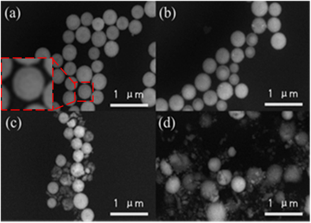
Figure 2. FESEM image of synthesized material with different temperature: (a) NN-350, (b) NN-400, (c) NNZ-500, (d) NNZ-600.
Download figure:
Standard image High-resolution imageXRD characterization was performed to check the crystalline phases of the samples (figure 3). All of the four samples showed the NiZn-oxide diffraction signals that can be indexed to the standard pattern of Ni0.6Zn0.4O (ICDD: 75–0273), with the peaks at about 36.9°, 42.8° and 62.2° agreeing with the (200), (220) and (102) crystal planes of Ni0.6Zn0.4O. The NN-350 sample is mostly of this Ni0.6Zn0.4O phase, with NiSe2 diffraction signals barely above the background level. With the annealing temperature increased to 400 °C, the NiSe2 phase become pretty clear, with the four peaks at 33.8°, 50.7°, 55.6° and 57.8° agreeing with the (210), (311), (023) and (321) crystal planes respectively (ICDD: 88–1711). The similarities between the 350 °C and 400 °C data can support the NN-350 contains a small amount of NiSe2 phase, and thus the sample is not really single phased.
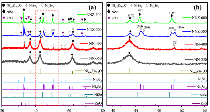
Figure 3. (a) XRD pattern of the materials synthesized at different temperatures and (b) partial enlarged details on 40°−56°.
Download figure:
Standard image High-resolution imageWith the temperature of reaction increased to 500 °C, three phases (Ni3Se4, Ni0.6Zn0.4O and ZnO) are observed in the NNZ-500 sample. Less Ni0.6Zn0.4O phase was found in the final product, while the rest of the Ni and Zn elements formed the relative nickel rich Ni3Se4 phase, with the peaks at about 33.1°, 33.6°, 44.8°, 45.3°, 50.2°, 50.7°, 60.3° and 61.9° agreeing with the ( ), (202), (
 ), (204), (002), (310), (
 ) and (
 ) crystal planes of Ni3Se4 (ICDD: 18–0890). Furthermore, the diffraction peaks of ZnO were also detected, as labeled out in the figure. The peaks at about 31.8°, 34.5°, 36,4°, 47.7°, 56.7°, 68.1° and 69.3° agreeing with the (100), (002), (101), (102), (110), (112) and (201) planes of ZnO (ICDD: 36–1451). As the temperature further increased to 600 °C, the three phases in the final product became NiSe, Ni0.6Zn0.4O and ZnO. The Ni0.6Zn0.4O peak intensities are further decreased in the NNZ-600 sample, and the nickel selenide became the more Ni rich phase of NiSe, with the peaks at about 32.8°, 44.4°, 49.8°, 59.6°, 60.9° and 68.9° agreeing with the (101), (102), (110), (103), (201) and (202) planes respectively (ICDD: 75–0610), and with the ZnO peak intensities increased from the level of the NNZ-500 sample. Overall, these temperature related phase distribution results agree with the SEM observation.
Upon heating, the ZnNi-gly template can release oxygen ions due to the pyrolysis of glycerol [17] which reacts with the Zn and Ni elements in the template to form Ni0.6Zn0.4O. Although surrounded by the Se vapour, at the low temperature of 350 °C, the vapour pressure and the reactivity of Se are relatively low, thus the final product is mostly Ni0.6Zn0.4O. Now that the heating rate in our sample preparation process is slow, all of our samples can be expected to pass through is Ni0.6Zn0.4O stage. With the annealing temperature increased, the vapour pressure and reactivity are increased to form nickel selenide phases, and on the other hand, the stability of Ni0.6Zn0.4O decreases at the higher temperature and can decompose to provide more Ni atoms to combine with Se. In our experiment, the more Ni supply at the higher temperatures appear to dominate, and thus the higher temperature, the more nickel rich nickel selenide phase is formed. As the nickel atoms diffuse out to react with the vapour to form nickel selenides, the hollow shell structure can be further promoted. For the Zinc atoms released from the Ni0.6Zn0.4O decomposition, it cannot react with vaporized selenium at our temperature range [28] thus it formed ZnO instead of zinc selenides. TEM characterization was further performed to investigate the NNZ-500 nanocomposite sample (figure 4). As shown in figure 4(a), the sample is mostly composed of hollow nanoshells, with partial of the spheres broken into pieces, agreeing with the SEM result in figure 2(c). The diameters of the nanoshells range from 200 to 300 nm, which agrees reasonably well with figure 2(c) within the error range. The particles imaged here are fewer than in the SEM image, thus larger and smaller spheres are not counted in this TEM image. With the higher image resolution of this TEM image, the surfaces of the nanoshell shells are observed to be rough, which is beneficial for providing increased surface area and rich active sites that can help improve the SC electrode performances. The existence of fractured structures may further help the electrolyte permeation and charge transport, and promote effective redox reactions, and enhance the electrochemical performance of the electrode material. The high-resolution TEM (HRTEM) image of NNZ-500 is obtained in the thin sample area of the fragments (figure 4(b)), where the interplanar spacings of 0.149, 0.19, 0.27 and 0.52 nm can be indexed to the (220) crystal plane of Ni0.6Zn0.4O, the (102) crystal plane of ZnO, and the (12) and (002) crystal planes of Ni3Se4, respectively. Figures. S1(a) and (b) are the partially enlarged view of the (102) crystal plane of Ni0.6Zn0.4O and the (102) crystal plane of ZnO. And the angle of Ni3Se4 ( ) and (002) crystal planes can be measured to 60°, which is equal to the calculation by following formula of the angle between crystal planes in monoclinic planes in monoclinic system:
where θ is the angle between the two crystal planes. (h1 k1 l1) and (h2 k2 l2) are the crystal face indices of the two crystal faces,d1 and d2 are the interplanar crystal spacing of the two crystal faces. (a), (b), (c) and β are the cell parameters of the monoclinic crystal system.

Figure 4. (a) TEM images of NNZ-500 nonastructure, (b) HRTEM images of ZONS-500, (c) selected area electron diffraction (SAED) pattern, (d) (e) EDS mapping of Ni, Zn, Se and O elements.
Download figure:
Standard image High-resolution imageFigure 4(c) shows the SAED pattern of the NNZ-500 sample, with the indexed ring curves showing the diffractions from the (220) crystal plane of Ni0.6Zn0.4O, the ( ) and (002) crystal planes of Ni3Se4, and the (102) and (002) crystal planes of ZnO, which further confirmed the polycrystalline structure of the NNZ-500 sample. Figure S2 further indexed the crystal planes of the bright spots that are not on the diffraction rings in figure 4(c). The SAED results and XRD results match very well. Moreover, EDS elemental mapping analysis (figures 4(d), (e)) revealed that the Ni, Zn, Se and O elements were relatively homogenously distributed in the NNZ-500 sample. In figure 4(e), the relatively fewer signal dots in the center of the spheres support the spheres are nanoshells. The slight differences in the element distributions support different phase distributions in the sample, with the Ni3Se4 rich region and Ni0.6Zn0.4O rich region discernable as indicated with the frames in the figure. In figure 4(d), the oval marked area is a Ni3Se4 rich region and the rectangle marked area is a Ni0.6Zn0.4O rich region. In the future, we will perform the TEM image of all of the samples to better understand their morphologies and crystalline structures.
The surface element compositions and chemical valence states of the NNZ-500 sample are investigated using XPS (figure 5). As shown in figure 5(a), 5 elements (C, O, Se, Ni and Zn) can be found on the surface of the sample. In figure 5(b), the two fitted XPS peaks of C 1s at 284.8 eV and 288.1 eV can be assigned to the carbon signal related to the C–C bond and the C–O bond respectively. The C–O peak mainly comes from the residue of the glycerate backbone after the high temperature pyrolysis [18, 29]. In figure 5(c), for the two spin–orbit doublet characteristic peaks, the peak at 291.1 eV can be corresponded to the O2− (Ni), and the peak at 231.2 eV can be corresponded to the O2− (Zn), respectively [30]. For the Se 3d signal in figure 5(d), the Se 3d3/2 and Se 3d5/2 peaks are located at the two locations of 55.3 eV and 54.7 eV due to spin–orbit splitting. And the other peak located at 59.1 eV could be assigned to oxidized Se (i.e. SeOx ), due to the oxidation of the Se atoms attached to the outermost surface of the nanoshell when exposed to air [31, 32]. As show in figure 5(e), the three peaks at 879.2 eV, 873.45 eV and 871.5 eV belong to Ni 2p1/2 and the other three peaks at 861.2 eV, 855.7 eV and 854.1 eV belong to Ni 2p3/2. Among them, because the binding energy of Ni3+ is higher than Ni2+, the peaks at 873.45 eV and 855.7 eV are assigned to Ni3+ and the peaks at 871.5 eV and 854.1 eV are assigned to Ni2+ [32]. Meanwhile, the two shake-up satellite peaks (marked as Sat.), having higher Binding Energy (∼15.5 eV) than the main peaks, are located at 879.2 eV and 861.2 eV respectively. For Zn 2p (figure 5(f)), the peaks at 1021.65 eV and 1044.5 eV are assigned to Zn 2p3/2 and Zn 2p1/2, and the ∼23 eV Binding Energy difference between these two peaks is in agreement with the Zn2+ state [33].

Figure 5. XPS spectra of NNZ-500 sample: (a) full spectrum, (b) C 1s, (c) O 1s, (d) Se 3d, (e) Ni 2p and (f) Zn 2p.
Download figure:
Standard image High-resolution imageThe electrochemical performance of the NN-350, NN-400, NNZ-500 and NNZ-600 samples are investigated in a three-electrode system. Figures 6(a) and S3(a) show the CV curves of the four samples obtained at a scan rate of 20 mV s−1, with a potential window of 0–0.5 V for NN-350, NN-400, NNZ-500 and −0.1 to 0.5 V for the NNZ-600 sample. Among them, NNZ-500 and NNZ-600 have similar redox peak positions and shapes, which is in accordance with their similar crystalline phase compositions. The fact that the NNZ-500 and NNZ-600 redox peaks are more outstanding to the background as compared with the NN-350 and NN-400 indicates NNZ-500 and NNZ-600 have stronger redox reaction processes. The nickel selenides, as battery-type materials [33], are the main contributors to the electrochemical performances of NNZ-500 and NNZ-600, while Ni0.6Zn0.4O, as a pseudo-capacitance material [34], is a main contributor to electrochemical performance in NN-350 and NN-400, when the concentrations of nickel selenides are relatively small. This is consistent with the XRD results. ZnO has a high theoretical specific capacity and its fibrolite-type space structure has good stability, thus the existence of the ZnO phase can also contribute the performance improvement of the NNZ-500 and NNZ-600 samples [30]. Different nickel selenide phases have different SC properties. NiSe2 as a semiconductor exhibited unsatisfactory electrochemistry properties, and NiSe2 nanoparticles only showed a specific capacity of 251 F g−1 in the literature [35, 36]. This explains the much lower electrochemical properties of the NN-400 sample as compared with the other samples. Compared the Ni3Se4 phase, the electrochemical properties of NiSe are reported to be slightly decreased [26, 37]. Furthermore, the substantial decrease in the specific capacitance of the NNZ-600 sample may be related to the extensive nanoshell structure breakdown in the sample, which remains to be further studied.

Figure 6. Electrochemical performances of NN-350, NN-400, NNZ-500 and NNZ-600: (a) CV curve of NNZ-500 at 20 mV s−1, (b) GCD curves at 1 A g−1, (c) specific capacities at different current densities, (d) cycling stability at the constant current density of 5 A g−1, (e)(f) EIS curves of different samples, inset image: equivalent circuit diagram.
Download figure:
Standard image High-resolution imageCV curves at different scan rates were investigated and the results were mathematically analyzed for further inquiry of the detailed energy storage mechanisms and reaction kinetics in NNZ-500. In figure. S3(b), CV curves of NNZ-500 at different scan rates (from 5 to 80 mV s−1) showed similar redox peak shapes. Clear redox peaks can be observed, indicating the charge/discharge mechanism belongs to battery type. As the scan rate increased, the peak intensity increased, and the peak positions shifted, which is caused by the increase in the overvoltage due to polarization [33]. From CV curve in figure 6(a), we calculated the capacitance of NNZ-500 is 1100 F g−1 at 20 mV s−1. It can be concluded that the sample has good reversibility and rate capability. And the electrode redox reaction process could be expressed by the following formula [29, 33, 38]:


In figure 6(b), the GCD curves of NN-350, NN-400, NNZ-500 and NNZ-600 at 1 A g−1 (potential window of 0–0.4 V) showed obvious charging and discharging platforms, and the position of the charge/discharge platform are in accordance with the positions of the redox peaks in the CV curves. The NNZ-500 sample showed the longest charge/discharge times, and we use the discharge curve to analyze the actual charge storage capacity of the material. The specific capacitances and discharge capacity of the samples can be calculated by the following formula:


In which i is the discharge current, Δt is the discharge time, m is the active electrode material weight and ΔV is the discharge voltage interval, respectively.
At 1 A g−1 current density, the specific capacitances of the NNZ-500 and NN-350 samples are 1089.2 F g−1 and 318.1 F g−1, respectively. Compared with the specific capacitance calculated from CV curve, there is an error of 0.955%. And the discharge capacity also can be calculated by equation (9). The NNZ-500 sample have a high capacity for 121.3 mAh g−1. As the discharge current density increased from 1 to 10 A g−1, the specific capacitance of the NNZ-500 sample is decreased to 790.5 F g−1, showing a good capacitance retention of 72.6% (figure 6(c)). In figure 6(d), it can also be found that the NNZ-500 sample further showed an excellent cycle stability (98.54% capacitance retention after 2000 cycles at 5 A g−1).
Note in the above specific capacitance calculations, the ΔV is the full discharge voltage interval, and the obtained specific capacitance is an 'average' value in that voltage range [39]. For smaller ΔV valves, the calculated specific capacitance values will be voltage dependent. There exists the proposal that the battery-type material cannot use the term 'pseudocapacitive' due to this specific capacitance value calculation issue [39]. However, this specific capacitance value calculation issue not only exists for the battery-type supercapacitor materials, but also exists for the EDLC-type material and the non-battery-type pseudocapacitive materials, unless the CV curve could be perfectly rectangular ( In a certain CV curve test, Δt/ΔV is kept constant, thus C ∝ I. A device with constant C will generate horizontal top and bottom lines in the CV loop. Any fluctuation in these lines would suggest capacitance change or extra potential generation in the electrode). Even for a battery-type material, as addressed later in this draft, there is still the significant capacitive contribution in the charge storage/release processes. As a practical tradition, it is recognized that battery-type electrode materials are still presented in the literature as pseudocapacitive materials [11, 39, 40]. Surely it will be safer to name them as energy storage materials.
In order to further analyze the electrical conductivity and reaction kinetics of the different samples, figures 6(e) and (f) present the Nyquist plots of the EIS characterizations, which can be analyzed with the equivalent series resistance (RΩ), charge-transfer resistance (Rct), constant phase element (CPE) and Warburg element (Zw) of the equivalent circuit model in figure 6(e) (inset) [41]. CPE is jointly controlled by CPE-P and CPE-T, and Zw is jointly controlled by W-R, W-T and W-P, as shown in the table S2. In the high-frequency region, the value of RΩ, which is the sum of the intrinsic resistance, electrolyte resistance and interfacial contact resistance, is determined by the abscissa intercept; and the value of Rct is determined by estimating the diameter of the semicircle [42]. According to the table S2, RΩ of the NNZ-500 sample is the lowest (0.74 Ω), indicating the most excellent electrical conductivity among the 4 samples. The NNZ-500 sample also showed a low charge transfer resistance of 1.13 Ω. Meanwhile, in the low-frequency region, the higher slope of the straight line represents the smaller value of the diffusion resistance and slope is controlled by Zw [43]. The straight line part of the NNZ-500 sample displayed the highest slope (figure 6(e)), which means the lowest diffusion resistance and the most excellent capacitance. All of these are consistent with the CV curves and GCD curves results.
In the investigation of SCs electrochemical behavior, understanding reaction kinetics is very important. The reaction kinetics of the electrode material charging and discharging process of the electrode material can be analyzed from the relationship between the peak current (i) and scan rate (v) of the CV curves [3]

where a and b are constants, and b can be obtained from the slope of log(i) versus log(v) data with linear fitting (figure 7(a)).

Figure 7. (a) The plots of log(i) against log(v) for NNZ-500 and (b) separation of the capacitive and diffusion-controlled currents of the NNZ-500 sample at a scan of 20 mV s−1.
Download figure:
Standard image High-resolution imageIf b = 1.0, it means the redox reaction is capacitive-controlled type; and if b = 0.5, it means the redox reaction is diffusion-controlled type. In figure 7(a), the two lines represent the NNZ-500 sample linear fitting results of the cathodic electrode (b = 0.59) and anodic electrode (b = 0.53), and the data obtained are overall within the error tolerance limits. Which indicate the charge storage process is mostly dominated by diffusion-controlled behavior.
The quantitative proportions of the two behaviors in the total reaction process can be obtained by analyzing the response current iv (V) [3, 44]

In which, iv (V) means the response current at a scan rate of v, under the potential of V, and v means the scan rate; k1 v and k2 v1/2 correspond with capacitive-controlled type current and diffusion-controlled type current, respectively.
Both sides of equation (11) are simultaneously divided by v1/2:

k1, k2 can be derived from the relationship between iv (V)/v1/2 and v1/2. Figure 7(b) shows iv (V), k1 v and k2 v1/2 of the ZONS-500 sample at a scan of 20 mV s−1. The capacitive-controlled and diffusion-controlled processes are about 39% and 61%, respectively. Further according to figure S4, by examining the contribution of the capacitive-controlled and diffusion-controlled processes at different scan rates, the results showed that the contribution of diffusion-controlled process contribution is decreased as the scan rate increased. Such diffusion-controlled process is a redox reaction process with intercalation of ions into the lattices. Thus, as the scan rate is increased, the time available for ion intercalation into the lattice is shortened, and eventually the contribution of the diffusion-controlled process can be decreased to a minor process, which is in agreement with the literature [44].
The excellent electrochemical performance of the NNZ-500 sample, among the 4 samples, can mainly be attributed to the following factors. Firstly, Ni3+ ions are highly electrophilic because of its partially filled d orbitals, which improves electron mobility, reduces electrical resistance, and increases the rate of surface redox reactions [45]. Secondly, the presence of elemental Se in the sample can have a positive effect on the rate performance and conductivity of the sample [46]. Thirdly, the multi-component active materials introduce more active sites, which is conducive to the redox on the electrode surface, thereby increasing the specific capacity [32]. Fourthly, the plentiful heterointerfaces can enable the active material to have a faster charge transfer rate [47]. And finally, the hollow nanoshell framework structure enlarges the specific surface area of the electrode material, which helps the electrolyte to get fully contacted to the active material, and improves the reaction kinetics, provides more charge storage sites and increases the specific capacitance of materials [7] as well as buffering the volume change and mechanical strain of the material, which improves the cycle stability. In the future, more experiment will be done to further manifest the relationship between the nanostructure and the specific surface area of the material.
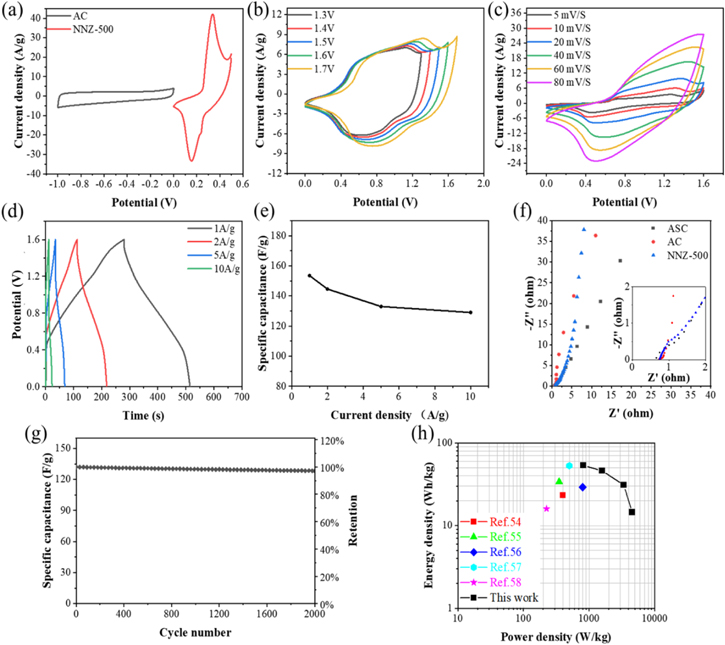
In order to further evaluate the practical application of the NNZ-500 material, an ASC device was assembled by using NNZ-500 as the positive electrode material and AC as the negative electrode material, and 3 M KOH as the electrolyte. CV curves at scan rate of 5–60 mV s−1 of the ASC device are shown in figure S5(a). In figure S5(b), The specific capacitance of the commercial AC electrode was measured to be 220.2 F g−1 at 1 A g−1. Refer to formula (1), the mass ratio of the NNZ-500 positive electrode and the AC negative electrode could be confirmed. Figure 8(a) showed the CV curves of the NNZ-500 positive electrode (potential window 0–0.5 V) and AC negative electrode (potential window −1 to 0 V) at a scan rate of 20 mV s−1. Figure 8(b) showed CV curves with the different potential windows (1.3 V to 1.7 V) at a scan rate of 20 mV s−1. Almost no apparent polarization can be found as the stable potential windows are extended to 1.6 V, while, at 1.7 V, there is a slight polarization induced current increase at the high voltage end. Therefore, the CV curves of ASC device were set at the 0–1.6 V potential window and at different scans rate of 5–80 mV s−1. Under the influence of the capacitive electrode, the CV curves of the device showed a rectangular-like shape under low scan rates. But as the scan rate is increased, the redox peak of the CV curve become more and more obvious, indicating that the battery-type electrode is playing a major role in it [48, 49]. The GCD curves showed obvious asymmetric capacitance characteristics of the device, and its charge and discharge curves all tend to be relatively straight, as shown in figure 8(d). And at the different current densities of 1 A g−1, 2 A g−1, 5 A g−1 and 10 A g−1, the specific capacitance of ASCs device was calculated to be 153.5 F g−1, 144 .6 F g−1, 133 .0 F g−1 and 129.1 F g−1, respectively, showing a rate capability of 84.3% at 10 A g−1 (figure 8(e)); and the discharge capacity of ASCs device was calculated to be 63.8 mAh g−1, 61.1 mAh g−1, 55.7 mAh g−1 and 51.4 mAh g−1, respectively. The Nyquist plots of the ASC device, the AC negative electrode and the NNZ-500 positive electrode were displayed in figure 8(f), where the RΩ values of 0.66 Ω, 0.72 Ω and 0.74 Ω can be obtained. Compared with the three-electrode system, the smallest RΩ values of the ASCs device originates from the full penetration of the electrolyte, into the electrode and through the diaphragm, and the reduced ion diffusion distance. However, the slope of the straight line of the device in the low-frequency region is relatively small, indicating the large diffusion resistance of the device. The assembled ASC device retained 98.6% of its capacity at 5 A g−1 after 2000 cycles, as shown in figure 8(g), which demonstrates extraordinary cycling stability. In the future, retention test with more cycles will be performed to better check the longer-term stability of the device. Meanwhile, to further analyze the electrochemical performance of the ASC device, figure 8(h) showed the Ragone plots of the ASC device to compare its power density and energy density. It possessed a high energy density of 53.4 Wh kg−1 at 819.0 W kg−1 and delivered a high-power density of 4539.2 W kg−1 at 14.5 Wh kg−1. Compared to those reported energy storage devices, including Ni3Se2//AC [50]. MoS2/NiSe2//AC [51] NiCoSe spheres//AC [52] ZnO/Ni3Se2//ZnO/Ni3Se2 [53] and ZnO/MnOx//AC [54] the superiority of the device in this work is obvious, especially for high energy densities. The excellent electrochemical performance with high power and energy density, and ultra-long cycling lifetime gives the device good potential for practical energy storage applications.
Figure 8. Electrochemical performance of the NNZ-500//AC ASC device, (a) CV curves of NNZ-500 and AC at 20 mV s−1, (b) CV curves at different potential windows, (c) CV curves at different scan rates, (d) GCD curves at different current densities, (e) specific capacitance at various current densities, (f) EIS plot of the NNZ-500, AC electrodes and ASC device, inset: enlarged image in the high frequency region, (g) cycle property of the ASC device, (h) the Ragone plot of the energy density versus power density curves.
Download figure:
Standard image High-resolution image
4. Conclusions
In summary, we have successfully synthesized three-phase nanocomposites of Ni3Se4, Ni0.6Zn0.4O, and ZnO, with a facile one step 'template-annealing' method, and investigated their electrochemical performance in three and two electrode systems. Among the samples, NNZ-500 displayed the best electrochemical properties. It exhibited the highest specific capacitance of 1089.2 F g−1 at 1 A g−1, a good rate capability of 72.6% capacitance retention from 1 to 10 A g−1, and excellent cycling stability of 98.54% capacitance retention after 2000 cycles at 5 A g−1 in three electrode systems. In addition, the ASC device of NNZ-500 and AC electrode possess a high energy density of 53.4 Wh kg−1 at 819.0 W kg−1 and retains 98.6% of its capacity at 5 A g−1 after 2000 cycles. Furthermore, two NNZ-500//AC ASCs devices connected in series are tested, which are able to light up a red LED for 10 min as shown in figure S6. Our work not only validates the advantages of the synergistic effect of transition metal selenide/oxide composites, but also provides new ideas for the synthesis and design of multiphase compounds for electrochemical energy storage device developments. In the future, more experiment will be done such as BET and AFM to further delve into the structure and properties of materials. The potential window of the current material is still relatively low, and the future research will also include the enlargement of the potential window.
Acknowledgments
This work was supported by the National Natural Science Foundation of China (21875066); Shanghai Leading Academic Discipline Project (B502); and the Shanghai Key Laboratory Project (08DZ2230500).
Data availability statement
The data generated and/or analysed during the current study are not publicly available for legal/ethical reasons but are available from the corresponding author on reasonable request.
Supplementary data (0.8 MB PDF)