
Abstract
GaSb is considered as an attractive p-type channel material for future III-V metal-oxide-semiconductor (MOS) technologies, but the processing conditions to utilize the full device potential such as low power logic applications and RF applications still need attention. In this work, applying rapid thermal annealing (RTA) to nanoscale GaSb vertical nanowire p-type MOS field-effect transistors, we have improved the average peak transconductance (gm,peak) by 50% among 28 devices and achieved 70 μS μm−1 at VDS = −0.5 V in a device with 200 nm gate length. In addition, a low subthreshold swing down to 144 mV dec−1 as well as an off-current below 5 nA μm−1 which refers to the off-current specification in low-operation-power condition has been obtained. Based on the statistical analysis, the results show a great enhancement in both on- and off-state performance with respect to previous work mainly due to the improved electrostatics and contacts after RTA, leading to a potential in low-power logic applications. We have also examined a short channel device with Lg = 80 nm in RTA, which shows an increased gm,peak up to 149 μS μm−1 at VDS = −0.5 V as well as a low on-resistance of 4.7 kΩ·μm. The potential of further enhancement in gm via RTA offers a good alternative to obtain high-performance devices for RF applications which have less stringent requirement for off-state performance. Our results indicate that post-fabrication annealing provides a great option to improve the performance of GaSb-based p-type devices with different structures for various applications.
Export citation and abstract BibTeX RIS

Original content from this work may be used under the terms of the Creative Commons Attribution 4.0 licence. Any further distribution of this work must maintain attribution to the author(s) and the title of the work, journal citation and DOI.
1. Introduction
III-V compound semiconductors are a promising channel material for the next generation high speed complementary-metal-oxide-semiconductor (CMOS) circuits thanks to their high carrier mobilities and injection velocities [1, 2]. High performance n-type metal-oxide-semiconductor field-effect transistors (MOSFETs) based on III-As materials, such as In(Ga)As [3, 4], have successfully demonstrated competitive on-state performance with respect to current Si-based n-MOSFETs. For their p-type counterpart, in spite of the high hole mobility in antimonides such as GaSb and InGaSb [2, 5], fabrication of GaSb-based p-MOSFETs with competitive performance is still challenging. III-V p-MOSFETs are mainly limited by gate-stack properties [6] and high-resistive, non-ohmic contacts [7] resulting in unbalanced performance in all-III-V CMOS technology [8–10]. Although one alternative with co-integration of conventional SiGe p-type and InGaAs n-type MOSFETs has been proposed [11, 12], the difficulty in material chemistry during processing may limit this type of device integration. Moreover, p-type GaSb play an essential role in heterostructure tunneling FETs [13] for emerging low power application. Thus, the motivation of further investigation and development of III-V p-type transistors still remains. Earlier studies based on (In)GaSb MOSFETs with various device structures [5, 14–17] have shown the challenge to retain the off-state performance when scaling from a long channel device to a short channel device (Lg < 500 nm). Thus, the trade-off between on- and off-state performance during gate length scaling therefore needs to be solved.
Recently, in a vertical nanowire (VNW) architecture using a gate-all-around (GAA) geometry, we have demonstrated GaSb VNW p-MOSFETs with improved electrostatic control and high transconductance [18, 19], as compared to other reported GaSb-related MOSFETs. Although an on/off current ratio of about 700 was demonstrated within 1.5 V gate voltage modulation in a 60 nm channel VNW devices [18], a further enhancement is doubtlessly required to approach low power logic applications. Rapid thermal annealing (RTA) is an important technique widely used in semiconductor device fabrication to improve the performance by influencing the material properties, such as dopant activation and defect passivation, as well as contacts improvement [20]. By annealing in a forming gas (N2/H2), the electrical properties at the interface between the semiconductor and gate oxides can be improved by the RTA process thanks to the passivation of interface defects (Dit), as reported for InGaAs n-channel devices [21]. Several investigations regarding contact improvement using RTA in n-MOSFETs have been also demonstrated, applied on both conventional planar devices [22] and nanoscale VNW MOSFETs [23]. In terms of GaSb-based technologies, it has been proven that the sheet resistance of Ni–GaSb can be lowered by RTA [24, 25] which may offer a possibility to improve the contact. However, for using RTA on the device level, only planar GaSb long channel (gate length Lg ≈ 5 μm) MOSFETs were reported by comparing individual device performance before and after annealing [17, 26], and it is not clear how the annealing affects the electrostatics and the contacts in short Lg devices.
In this work, we for the first time apply post fabrication RTA to nanoscale GaSb VNW transistors with two different device structures (sample 1:200 nm Lg with Ni top contact; sample 2:80 nm Lg with W top contact) and achieve substantial improvements in transistor performance in both samples. Section 3.1 mainly discusses the on-state performance in the different samples with varying RTA temperatures. Section 3.2 focuses on the influence of RTA on the on-resistance (Ron) while section 3.3 discusses the annealing effects on the electrostatics and off-state performance. Finally, a further discussion and the corresponding benchmark will be shown in section 3.4 Our statistical results in this study reveal that RTA can be used as a device performance booster for GaSb p-type transistors in order to reach a specific application.
2. Experimental methods
InAs-GaSb NWs were grown on a prepatterned Si substrate with a 260 nm n+-InAs buffer layer by metal-organic vapor-phase epitaxy (MOVPE) via vapor–liquid–solid process. InAs buffer layer was used for the integration of III-V materials on Si substrates. The NW growth started with a short n-type InAs stem doped with Sn to not only enable nucleation of GaSb NW growth, but also form the source of the device, which has an InAs/GaSb broken band tunneling junction to assist the carrier transport [27]. Subsequently, undoped GaSb with an estimated background doping of ∼1016 cm−3 and p-type GaSb NWs doped with Zn (molar fractions: χTMGa = 4.9 × 10⁻⁵, χTMSb = 5.6 × 10⁻⁵, DEZn/TMGa = 0.39) were grown for the channel and the drain, respectively. Here, two samples with different structures as well as process schemes were fabricated and compared. Sample 1 (S1) was grown as the above structure and fabricated with a gate-first process starting from the NW bottom. In contrast, a gate-last process starting from the top contact of the NW transistors was employed for sample 2 (S2) which has a 2 nm thick Sn-doped InAs shell as an interfacial layer for the top (drain) contact.
The device fabrication for S1 was initialized by the digital etching while the first step for S2 was the drain contact which requires several additional steps discussed below. Firstly, a 20 nm thick Al2O3 was deposited by atomic layer deposition (ALD) as the first spacer which was then removed in the drain region of the NW MOSFET. The length of the drain was defined by a back-etch process with S1813 (photoresist). Next, the drain contact was formed by sputtering 20 nm W which was dry etched anisotropically leaving metal only on the NW sidewalls. The S1813 was further thinned down to define the gate length. Then the Al2O3 on the channel region was wet etched and S1813 removed. Next, the diameter of the GaSb channel was reduced by ∼10 nm and ∼20 nm in S1 and S2, respectively, using repeated digital etching with oxidation inside an oxygen chamber followed by an oxide etch in HCl:IPA (1:10) for 30 s. In the case of S2, the oxidation for the first cycle of digital etch was carried out in an ozone ambient for 30 s at 50 °C to fully oxidize the InAs shell. A bilayer high-k film with 1 nm Al2O3/3 nm HfO2 (EOT  1 nm) was deposited using ALD. For S1, an extra 20 nm Al2O3 layer was grown after the high-k film as the first spacer whose height was defined by the same back-etch process using S1813. The remaining fabrication steps were identical for two samples. A 60 nm W was sputtered for the gate metal and the excess gate-metal was subsequently removed using S1813 mask and dry etching. The gate length in S1 was defined in this step. Both the NW diameter of the channel and the gate length in S1 and S2 were verified by the scanning electron microscopy (SEM) image shown in figures 1(a) and (b), respectively. The samples were finalized by the second spacer deposition and the contact metallization.
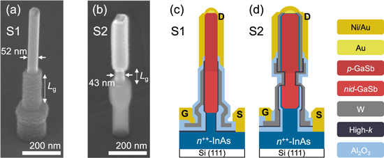
Figure 1. SEM images of the real NW devices: (a) a device in S1 with Lg = 200 nm after gate length definition; (b) a device in S2 with Lg = 80 nm after high-k deposition. The marked diameters include the channel diameter and the high-k thickness (4 nm). Schematics of the GaSb single NW transistor are displayed in (c) S1 and (d) S2. G, S and D denote gate, source and drain, respectively. nid represents non-intentionally doping.
Download figure:
Standard image High-resolution imageFigures 1(c) and (d) illustrate the schematics of the final NW transistor in S1 and S2, respectively. In order to enable post processing annealing of the samples at high temperatures, all the spacers for isolating the terminals are replaced with Al2O3 rather than polymers which were usually used as the second spacer in our previous work [10, 28]. After initial electrical characterizations for the devices, an RTA process was performed in wall-mounted rapid thermal processing (RTP) system, RTP-1200-100, from UniTemp GmbH, with a forming gas (N2/H2, 95%/5%) for 2 min at temperatures from 200 °C to 350 °C for S1 and 250 °C to 350 °C for S2. Two step temperature ramping scheme (the temperature first increases to 50 °C less than the setpoint in 30 s and stabilizes for 20 s. Then the temperature continues increasing by a ramping rate of 1.67 °C s−1 to the target.) was employed in order to avoid the temperature overshooting. When it reaches the desirable temperature, 2 min is waited before cooling down without supplying any power on the heater. Devices were electrically characterized sequentially after each RTA process. The main information and differences between two samples are summarized in table 1. All the devices in this work are based on single NW transistors. In S2, the highly doped GaSb/InAs core/shell structure in the drain combined with the W–InAs contact can help to lower the resistivity [29, 30].
Table 1. Differences in device structures between two samples.
| No. | Process sequence | Top contact | Lg | Channel diameter | RTA |
|---|---|---|---|---|---|
| Sample 1 (S1) | Gate-first | Ni/p-GaSb | 200 nm | 44 nm | 200 °C–350 °C |
| Sample 2 (S2) | Gate-last | W/n-InAs/p-GaSb | 80 nm | 35 nm | 250 °C–350 °C |
3. Results and discussion
3.1. Transistor on-state performance improved by RTA
The transfer characteristics of the individual GaSb NW MOSFET in each sample before and after RTA at different temperatures are shown in figure 2. In consideration of the change in threshold voltage (VT) after RTA (see supplementary material: figure S1 (available online at stacks.iop.org/NANO/33/075202/mmedia)), the gate overdrive voltage, VOV = VGS–VT, is presented in this article instead of the absolute gate bias VGS for better comparison. Generally, as compared to the as-fabricated device performance, the drain current (IDS) as well as gm increases after RTA and reaches a maximum after annealing at 300 °C in both samples. Further increasing the RTA temperature up to 350 °C, however, degrades the on-state performance in both samples. In S1, an increased on-current (Ion, defined at VOV = −0.5 V) of 31 μA μm−1 as well as a peak gm (gm,peak) of 70 μS μm−1 at VDS = −0.5 V are achieved in the device after RTA at 300 °C with corresponding increment of ∼25% as shown in figures 2(a) and (b), respectively. However, the source depletion of the device in S1 becomes severe after annealing at 350 °C probably due to higher efficiency in hydrogen passivation at the InAs/high-k interface than that in GaSb/high-k interface so that InAs bands adjacent to the junction move up faster than GaSb bands at high negative gate bias. As a result, the tunneling probability between InAs and GaSb may be reduced, thereby lowering the drain current. Despite a thicker oxide layer including both the high-k and the bottom spacer (Al2O3) on the InAs segment, substantially lower Dit at the interface of InAs/high-k likely results in high gating efficiency at high gate voltage. Several reports have shown that the optimal annealing temperature of hydrogen passivation of In(Ga)As/high-k interface is close to 350 °C [31, 32]. Therefore, annealing at lower temperatures has relatively limited effects on InAs/high-k interface passivation, resulting in less source depletion.

Figure 2. Transfer characteristics of (a), (b) S1 and (c), (d) S2 before (as-fabricated) and after RTA at different temperatures. Here, an overdrive voltage VOV = VGS–VT is used to align VGS = VT to 0 in all the cases. IDS–VOV are shown in (a) and (c) while gm–VOV are shown in (b) and (d). Ion is defined at VOV = −0.5 V and −0.7 V for S1 and S2, respectively. The reason of using different VOV for Ion definition is to keep the identical gate bias (0.2 V) away from the position of as-fabricated gm,peak in both samples as shown in figures.
Download figure:
Standard image High-resolution imageThanks to a shorter Lg, S2 provides a better on-state performance in both IDS and gm,peak, but meanwhile higher overdrive bias (∼0.2 V higher in VOV) is needed to achieve gm,peak as compared to S1, seen in figures 2(b) and (d). Thus, to reflect this difference, we defined Ion at relatively higher VOV (−0.7 V) for S2. Here, as the comparison of Ion only occurs before and after RTA in the same sample, Ion may well be defined independently between two samples. In S2, despite only 20% increase in Ion, gm,peak is enhanced by almost 50% up to 149 μS μm−1 after RTA at 300 °C.
Figure 3 shows the corresponding statistical results based on 28 single NW devices in both S1 and S2, as a function of RTA temperatures. In the case of S1, the median values of Ion and gm,peak determined at different RTA temperatures are compared in figures 3(a) and (b), respectively, showing an unambiguous enhancement with increasing the annealing temperature from 200 °C to 300 °C whereas maintaining almost the same value when further increasing the temperature to 350 °C. In figure 3(b), gm,peak increases 50% on average after RTA at 300 °C compared to as-fabricated devices, reaching a maximum median value of 42 μS μm−1. It is noticeable that when increasing the RTA temperature, the minimum gm,peak increases more than 100% and it follows the same trend as the median value while the maximum gm,peak increases roughly 10%. Therefore, the gm,peak increase mainly results from the enhancement in those devices with low as-fabricated gm,peak. However, after annealing at 350 °C, those devices start degrading again, resulting in a reduced minimum value in both Ion and gm,peak. Thus, the spread of the data set after annealing at 300 °C is narrowed but widened again when annealing at 350 °C due to the device degradation. In addition, a similar feature of Ion change with the RTA temperature is shown in figure 3(a).
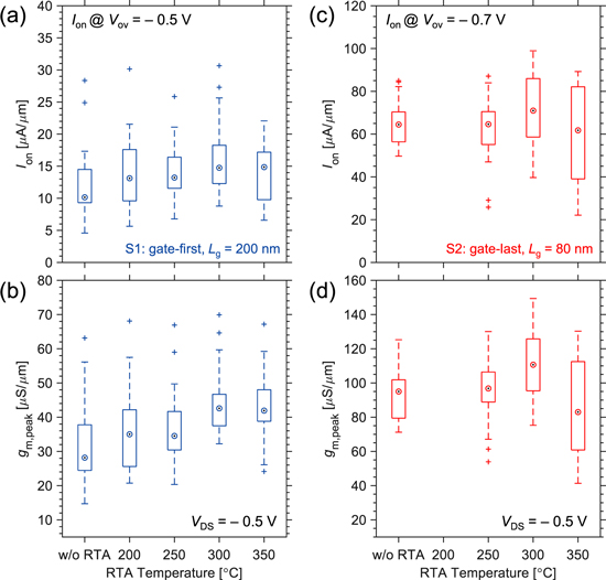
Figure 3. Statistics of (a), (c) Ion and (b), (d) gm,peak as a function of RTA temperatures in (a), (b) S1 and (c), (d) S2. Data are shown in a boxplot based on 28 devices in each sample. The same dataset for all other figures in this article. VDS = −0.5 V for all plots.
Download figure:
Standard image High-resolution image3.2. Annealing effects on Ron
Figure 4(a) compares the output characteristics of the same devices plotted in figure 2 before and after RTA. Here, only the output curve at VOV that defines Ion is selected to present for both samples, respectively. For the individual devices in S1 and S2, Ron first decreases when annealing at 300 °C, reaching 16.7 kΩ·μm and 4.7 kΩ·μm in the device of S1 and S2, respectively, but increases again after RTA at 350 °C. Similar as the individual devices, the corresponding statistical result of Ron in S1 shows decreasing Ron as increasing the RTA temperature until 300 °C, presented in figure 4(b). In spite of the large variation in Ron, it is found that the median Ron of all devices annealed at 300 °C is still reduced 26% as compared to that without annealing. In contrast to the clear drop in Ron after RTA observed in S1, no noticeable change of Ron is observed in S2 in the same RTA temperature interval, shown in figure 4(c). Instead, almost identical median value and device variation are obtained with increasing RTA temperature until 300 °C. Among the 28 studied devices in S2, there are 12 devices with a higher Ron after RTA at 300 °C and 16 devices having a lower value. Although the maximum reduction reaches 33%, most of the devices have a change within ±10%, leading to a similar median value after RTA. As compared to S1, a 7-times lower mean Ron (6.5 kΩ·μm) is achieved before annealing in S2, while the gate length is only 2.5 times shorter. Hence, the top contact is likely improved with W–InAs/GaSb configuration, thereby contributing to significant Ron reduction in S2.

Figure 4. Annealing effects on (a) output characteristics of the same device in figure 2 at the gate bias which is used to define Ion in S1 and S2. (b) and (c) show the statistics with boxplots of Ron as a function of RTA temperature in S1 and S2, respectively.
Download figure:
Standard image High-resolution imageIt is reasonable to assume that the access resistance will remain constant when annealing at such moderate temperatures (200 °C–350 °C). The access resistance is mainly determined by the geometry and the carrier density, which relates to the doping concentration in this case. Since the epitaxial growth temperature of the NWs is much higher than the annealing temperatures, the doping profile should be unchanged after RTA. Therefore, we believe that the Ron reduction in S1 after RTA can be mainly interpreted as the improvement of the top contact in the NW transistors. Annealing can promote Ni to alloy with GaSb, leading to more Ni–GaSb alloy formed at high temperature thus lowering the sheet resistance of Ni–GaSb alloy layer [7, 24]. Extrapolating to the transistor level, the contact resistance can be lowered by forming higher conducting Ni–GaSb alloy after annealing. However, higher annealing temperatures may degrade the contact attributed to the presence of a new phase Ni2Ga3 (forming at 369 °C according to the phase diagram [33] with higher resistivity in the alloy while the desired NiGa(Sb) phase is only formed at relatively low annealing temperature [25]. Consequently, a slight increase in Ron occurs after RTA at 350 °C in S1.
Despite unchanged median value and variation in statistical result of Ron in S2, a small variance within 10% is still found in most of the devices. Ron increasing or decreasing in this case could be attributed to the relatively slight change in the top contact which is W–InAs/GaSb in S2. W is used as a non-alloy ohmic contact for InGaAs transistors [4] and behaves similarly as Mo [28] for contacting InGaAs. Moreover, a recent study on InGaAs VNW devices with Mo–InGaAs (similar as W–InGaAs) non-alloy contact shows a smaller change in Ron with varying RTA temperatures as compared to Ni–InGaAs transistors [23]. Thus, W–InAs/GaSb likely provides a rather thermally stable contact below 300 °C as compared to Ni–GaSb. However, we observed a dramatic increase in not only the median value but the spread of Ron after RTA at 350 °C, which may highly relate to the deterioration in channel interface thus leading to a dominantly large channel resistance as compared to considerably low contact resistance in S2. The annealing effects on the interface will be discussed in the next section
3.3. Annealing effects on electrostatics and off-state performance
Figure 5(a) presents the statistics of saturation SS (SSsat, at VDS = −0.5 V) with varying RTA temperature. For S1, SSsat continuously reduces when increasing the annealing temperature even up to 350 °C. Specifically, the reduction in SSsat is mainly determined by the improvement of devices with originally high SS, thus a narrower distribution is achieved, reaching a lowest SSsat = 166 mV dec−1 in a device as shown in figure 5(b). A similar trend based on statistics is observed for SSlin (see supplementary material: figure S2(a)) and a minimum value of 144 mV dec−1 is obtained in the same device shown in figure 5(b), which is the lowest subthreshold swing among reported GaSb-based p-MOSFETs [8, 17, 19, 34]. In accordance with the equation [35]  where k is the Boltzmann constant, T the temperature, q the electron charge and Cox the capacitance of the high-k oxides which is assumed to be invariant with annealing [36]. Dit refers to the trap density of the MOS interface, usually describing the interface quality. The lower Dit, the better interface quality. Based on this equation, the change of SS can be determined by Dit only. Thus, we estimated Dit ≈ 3.6 × 10¹³ eV−1 cm−2 at VDS = −0.05 V after annealing by calculating a coaxial oxide capacitance of Cox ≈ 7 aF nm−1. By considering the same device before annealing, Dit approximates to 4.4 × 10¹³ eV−1 cm−2, thus indicating a reduction of 22%. Therefore, the reduction in SS can originate from the MOS interface improvement by lowering Dit attributed to the H2 passivation capability during RTA.

Figure 5. Annealing effects on electrostatics and the off-state performance. (a) Statistics of SSsat in both samples. Y-axis is plotted in logarithm. (b) Transfer characteristics of the device with lowest SS and highest Ion/Ioff at VDS = −0.5 V in S1. Ion is defined at VOV = −0.5 V while Ioff is defined at VOV = 0.5 V. Statistics of (b) Ioff and minimum IDS at off-state in the range of 0 V < VGS < 1 V, as well as (c) on/off current ratio Ion/Ioff in S1.
Download figure:
Standard image High-resolution imageIn contrast, S2 exhibits an opposite trend of SSsat (also see SSlin trend in supplementary material: figure S2(a)) with RTA temperature, showing a significant increase after annealing at 300 °C–350 °C. Although S2 has a higher SSsat than S1 before RTA, a similar drain-induced barrier lowering is found in S1 and S2, suggesting a good electrostatic control without short channel effect when scaling down Lg from 200 to 80 nm. Therefore, the high SS before RTA in S2 mainly results from the increase of Dit at the channel interface as compared to that of S1 fabricated with the gate-first process. For the gate-last process in S2, many additional steps are required prior to the digital etching and subsequent high-k deposition, resulting in unexpected process-induced contaminations. One likely contamination of the channel can be oxygen vacancy from residual GaSb oxides present from the digital etching. The first 30 s ozone treatment at 50 °C is likely to oxidate through the InAs shell and deeply penetrate into GaSb to form a thick GaSb oxide layer [37] which may be insufficiently etched by HCl:IPA for 30 s in the current process. The presence of oxygen vacancy at the interface may generate more traps at the GaSb/high-k interface thereby increasing SS. Although these oxygen vacancies might be reduced by annealing in an ambient with hydrogen, other possible contamination originating from the previous process would be active to react with the channel surface when annealing, probably leading to more interface states. Thus, the dramatic increase of SS after RTA is likely related to these interface states activated by annealing. As a result, Dit increases substantially after RTA at 300 °C or higher, leading to a poor off-state performance. Further detailed material characterizations for the channel interface in our NWs, such as x-ray photoelectron spectroscopy and transmission electron microscopy, are needed to verify of our hypothesis.
The off-state performance in S1 is further studied. The device with lowest SS after RTA at 350 °C also reveals a high on/off current ratio (Ion/Ioff) over 1000 with attractive Ion = 23 μA μm−1 and a low Ioff = 19 nA μm−1 at VDS = −0.5 V, as demonstrated in figure 5(b). In figure 5(c), a stable Ioff = 40 nA μm−1 retains until annealing at 300 °C and further reduces to 30 nA μm−1 after RTA 350 °C. In addition, the minimum drain current (IDS,min) fluctuates with RTA temperatures in a small range around ∼10 nA μm−1. The lowest IDS,min in all studied devices at off-state reaches 4 nA μm−1 after annealing at 200 °C and 250 °C, which fulfills the Ioff specification of the International Technology Roadmap for Semiconductors low operation power application (5 nA μm−1) [38]. In addition, approximately 50% increase in Ion/Ioff is attained after RTA at 350 °C attributed to both Ion increase and Ioff reduction with respect to as-fabricated performance as shown in figure 5(d). On the other hand, only Ion increase accounts for the gradual increase in Ion/Ioff when the annealing at 200 °C–300 °C. The results of S1 show the best balance in on- and off-state performance among recently reported GaSb-related transistors [10, 18, 39], indicating an attractive potential for low power logic applications. In contrast, the off-state performance degrades significantly after RTA process in S2 as both SS and Ioff (see supplementary material: figure S2(b)) increase with annealing temperatures.
3.4. Discussion and benchmarking
Based on the analysis in the previous sections, it is evident that RTA at 300 °C provides the best performance improvement with annealing in both S1 and S2. Thus, table 2 summarizes the improvements and changes in each sample after RTA at 300 °C with respect to the as-fabricated performance. For S1, the improvements of not only the top contact but the channel interface after RTA lead to the reduction in both Ron and SS, thus in turn contributing to an enhancement of gm,peak by 50% on average. Surprisingly, for S2, gm,peak achieves 20% increment after annealing whereas Ron keeps invariant and SS deteriorates due to more unexpected contamination in S2. In spite of an invariant Ron on average, slight change still exists in individual devices (see supplementary material), where those devices with reduced Ron, the gm,peak increase linearly depends on the reduction in Ron. Therefore, the reduction of Ron could be the unique contribution to the gm,peak increase, leading to less improvement in percentage of gm,peak for S2 as compared to S1. The detailed correlation of gm,peak, Ron and SS regarding on individual devices in both samples is shown in supplementary material: figures S3 and S4.
Table 2. Summary of the RTA effects on S1 and S2 by comparing the difference before and after RTA at 300 °C.
| Ave. change | gm,peak | Ion | Ron | SSlin / SSsat |
|---|---|---|---|---|
| S1: gate-first | +50% | +47% | −26% | −10%/−9% |
| S2: gate-last | +20% | +9% | 0% | +30/+31% |
The average change reflects the similar conclusions as discussed previously. For S1, it is difficult to significantly improve the top contact and channel interface at the same since effectively improving MOS interface usually requires a higher annealing temperature (approximately 350 °C) [40, 41], which could degrade the top contact of the device (increasing Ron) by changing the Ni–GaSb alloy structures as addressed previously. One feasible option to further improve GaSb NW MOSFETs by annealing is probably to include both forming gas (N2/H2) annealing directly after gate metal deposition for the MOS interface at a higher temperature and another annealing process at a relatively lower temperature after fabrication to only improve the contacts [41]. For S2, the key issue is the high SS which likely results from the process-induced contamination, being strongly degraded by RTA. However, the impressive improvement in gm exists in those devices with high as-fabricated performance in S2. Thus, although using the characteristics of S2 for digital applications may be challenging, for some RF applications [28] or the current source of all-III-V platform, a high SS can still be acceptable. Further gate-stack development can also help to improve SS.
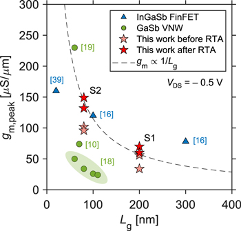
Table 3 and figure 6 benchmark this work with recently published GaSb-related p-type MOSFETs with Lg < 500 nm. 3 different VNW devices from S1 after annealing are included in table 3, all showing a good off-state current below 10 nA μm−1 simultaneously along with a competitive Ion, showing a great balance in on- and off-state performance. We have also achieved a record SS among all GaSb-based sub-500 nm p-type MOSFETs, verifying a great electrostatic control with the gate-first process. For the benchmarking of gm,peak versus Lg in figure 6, comparing to the performance of not annealed devices, the annealed devices in both S1 and S2 have been improved and both approach the position in line with the gate length scaling in state-of-the-art GaSb-based transistors.
Table 3. Benchmarking devices in S1 with other published GaSb-based p-type MOSFETs at VDS = −0.5 V. Blank spaces are due to incomplete data.
| S1 in this work | IEDM18 [19] | TED2020 [18] | IEDM17 [39] | IEDM15 [8] | ||||
|---|---|---|---|---|---|---|---|---|
| Structure | VNW-1 | VNW-2 | VNW-3 | VNW | VNW-1 | VNW-2 | FinFET a | LNS b |
| Lg (nm) | 200 | 200 | 200 | 60 | 110 | 60 | 20 | 500 |
| Diameter (nm) | 44 | 44 | 44 | 22 | 24 | 24 | 10 | 20 |
| SSlin (mV dec−1) | 144 | 157 | 162 | 175 | 224 | 260 | 217 | |
| SSsat (mV dec−1) | 166 | 189 | 175 | 305 | 216 | 188 | ||
| IDS,min (nA μm−1) | 9 | 9 | 4 | ∼3000 | ∼4 | 28 | ∼2000 | 5 |
| Ion at VGS = −0.5 V (μA μm−1) | 23 | 31 | 16 | 98 | 3 | 20 | 100 | ∼10 |
| Ion/Ioff with ΔVGS = 1 V | 1190 | 980 | 1210 | ∼30 | ∼750 | 330 | 50 | ∼2000 |
Figure 6. Benchmarking gm,peak versus Lg of the devices in this work and other GaSb-based p-FETs. Stars represent the present work which is in line with state-of-the-art GaSb-based devices after annealing.
Download figure:
Standard image High-resolution image
4. Conclusion
We have demonstrated that annealing improves the on-state performance of nanoscale GaSb vertical NW p-MOSFETs on Si with two different structures by RTA. The statistical results show that 50% and 20% increase in gm,peak are achieved in S1 (Lg = 200 nm) and S2 (Lg = 80 nm), respectively. We also found that the device structure and processing sequence strongly affect the off-state performance after RTA. For S1, a good off-state is obtained before RTA and remains unchanged after annealing, resulting in an increased on/off current ratio and a low SS thanks to the improvement in on-current and channel interface quality, respectively. The results suggest a great balance in on- and off-state performance among all reported sub-500 nm GaSb-based transistors, leading to an attractive potential for III-V based low power logic applications. However, in the case of S2, SS strongly increases after RTA probably due to the formation of interface traps during annealing, causing a severe degradation in off-state performance. Despite this, by the means of RTA, a remarkably further enhancement of gm,peak in the devices with as-fabricated high performance is noticed. Thus, RTA can be used as an approach to increase gm for devices with potential use in III-V RF applications. Our work suggests that the use RTA can be a good strategy to further improve the performance of nanoscale GaSb-based p-type devices with various structures for different applications based on III-V platform technologies.
Acknowledgments
This work was supported by the Swedish Research Council (VR), and the Swedish Foundation for Strategic Research (SSF).
Data availability statement
The data that support the findings of this study are available upon reasonable request from the authors.