
Abstract
This work presents a H2S selective resistive gas sensor design based on a chemical field effect transistor (ChemFET) with open gate formed by hundreds of high temperature chemical vapour deposition (CVD) grown zinc oxide nanowires (ZnO NW). The sensing ability of pristine ZnO NWs and surface functionalized ZnO NWs for H2S is analysed systematically. ZnO NWs are functionalized by deposition of discontinuous gold (Au) nanoparticle films of different thicknesses of catalyst layer ranging from 1 to 10 nm and are compared in their gas sensing properties. All experiments were performed in a temperature stabilized small volume compartment with adjustable gas mixture at room temperature. The results allow for a well-founded understanding of signal-to-noise ratio, enhanced response, and improved limit of detection due to the Au functionalisation. Comprehension and controlled application of the beneficial effects of Au catalyst on ZnO NWs allow for the detection of very low H2S concentrations down to 10 ppb, and a theoretically estimated 500 ppt in synthetic air at room temperature.
Export citation and abstract BibTeX RIS

Original content from this work may be used under the terms of the Creative Commons Attribution 4.0 licence. Any further distribution of this work must maintain attribution to the author(s) and the title of the work, journal citation and DOI.
1. Introduction
Hydrogen sulphide (H2S), a colourless and highly toxic gas mainly released as a side product in oil refinery processes and fossil combustion [1] or simply during the decomposition of organic compounds, is highly dangerous to human's health at a concentration level of only 3–10 ppm and above [2–4]. Patients exposed to H2S face persistent symptoms and irreversible side effects in their respiratory system, and most organs are susceptible to the effects of H2S exposure [2], which is easily highlighting H2S as a broad spectrum toxicant and a serious lethal threat in occupational poisoning [5].
On the other hand, H2S is a by-product of the human metabolism itself and hence is found in chemical compositions of the human body. Exhaled human breath is containing a mixture of nitrogen, oxygen and carbon dioxide alongside with numerous volatile organic compounds (VOC) and sulphides, like H2S, at trace amount (ppt—ppb). Exhaled concentrations of H2S in expired breath are successfully linked to human diseases and therefore suggest H2S as a potent biomarker. Millonig et al have shown in 2010 how gastroesophageal cancer correlates to an exhaled H2S concentration of  which was detected via ion-molecule reaction-mass spectrometry [6–8]. Zhang et al linked the endogenous H2S levels in exhaled breath to airway inflammation in patients with chronic persistent asthma. In their study, 57 eosinophilic asthma patients were exhaling
  of H2S, and 40 paucigranulocytic asthma patients
  of H2S on average, which was prevailed in the last portion of deep breaths [9, 10].
To fulfil the task of monitoring and detecting H2S at such low concentrations, advanced sensors with enhanced gas sensing properties are required in both non-biological systems (ppm range) and biological systems (ppt—ppb range) [11]. A standard approach is the use of mass spectrometry and gas chromatography, which allow a reliable and selective detection of low gaseous concentrations [12, 13]. However, instruments for these techniques are often bulky and expensive [13], which prohibits mobile application. For detection by IR adsorption, H2S has first to be converted into SO2 by UV irradiation [14] to become detectable. Moreover, preparation of samples that are suitable for medical breath analysis, such as big volume samples of water vapour filtered exhaled breath, appears to be challenging.
A more recent and simple solution considers the electronic nose (eNose) approach based on an array of a gas sensors. Here, the focus is on the usage of nanomaterials, such as noble metals and metal oxides, for chemiresistive gas sensors that offer a large specific surface area, porosity, fast response, and cost effective production [15]. In the 60s T. Seiyama et al already introduced the detection principle of metal oxides by using ZnO thin films at operating temperatures around  to detect propane and CO2 at concentrations down to
  [16]. Gregis et al presented an inexpensive medical analysis of VOCs related to lung cancer by using a miniaturized gas chromatographic device based on a single metal oxide gas sensor. Among other VOCs, Toluene was successfully detected at a level of
  even in the presence of water vapour in synthetic air [17]. In another work, Wang et al investigated a gas sensor based on ZnO nanorods synthesized by hydrothermal growth, exhibiting a significant response and good selectivity down to
  of H2S at room temperature [18].
Chemiresistive gas sensors can be based on pristine standalone metal oxides or on heterojunctions consisting of several metal oxides [19]. In some studies doped and surface modified metal oxides were considered [20]. Feng et al demonstrated how especially gold modified ZnO nanoplates can enhance the response towards several types of VOCs by 2–9 times, and Sharma et al towards H2S in particular [21, 22]. Especially, ZnO is a particularly suitable metal oxide candidate due to its exceptional semiconducting and nanoelectronic properties. Controlled and cost-efficient growth allows for the formation of nanofibers, nanopods, nanobelts and nanorods of different dimensions [20, 21]. These sensors offer a good platform for the fabrication of highly efficient H2S sensing devices [6].
In this work, we investigate sensing of H2S at ppb level with ZnO NWs grown by a high temperature CVD process yielding high quality and high purity ZnO structures, and the effect of surface functionalisation with gold nanoparticle films by magnetron sputtering. We study in detail which sensing parameters are enhanced due to the catalyst addition, and how different catalyst loadings alter the sensing behaviour of pristine ZnO towards H2S. We find that Au-modified ZnO can detect  of H2S in synthetic air at room temperature with an estimated limit of detection (
 ) of
) of 
2. Experimental
2.1. Growth of ZnO nanowires
The ZnO NWs used here were grown by high temperature CVD using the vapour liquid solid (VLS) method [23] in a three zone tube furnace. For the growth,  of a mixture of ZnO (
 purity) and carbon powder (molar ratio of ZnO to C was 1:1) was placed inside a quartz boat and positioned inside the furnace at a nominal temperature of
  at a pressure of
  The substrate, a
  silicon (100) wafer piece with a
  thick catalytic gold (Au) layer on top, was positioned
  downstream of the source material inside the liner tube of the furnace at a temperature of
  During the
  of the growth process, evaporated ZnO(g) was transported via an argon carrier gas (Ar,
 purity) towards the oxygen inlet (O2
 purity diluted in Ar down to
 ) which was positioned
  upstream of the substrate. The catalytic gold film melts at the beginning of the process and forms Zn saturated Au/Zn droplets. Ongoing oxidation of the Au/Zn alloy then forms a dense forest of 80–100 nm thin and up to
  long nanowires. Scanning electron micrograph in figures 1(a)–(b) shows an example of such a dense ZnO NW forest.

Figure 1. Scanning electron micrographs of pristine ZnO NWs (a)–(b) as-grown by CVD on silicon (100) and (c) evenly distributed and aligned via dielectrophoresis on the sensor bridging the 5 μm gap between the parallel Ti/Au electrode pads.
Download figure:
Standard image High-resolution imageA detailed analysis of the ZnO NW growth process and an in-depth analysis of the ZnO NW properties were reported by Li et al [24].
2.2. Gas sensor fabrication and Au functionalisation of ZnO NWs
Sensors were fabricated by deposition of ZnO NWs on top of a planar titanium/gold (Ti/Au) contact structure on a silicon substrate with  of insulating SiO2 on top. The two parallel electrodes were
  long and separated on average by a
  gap. This gap was bridged with pristine ZnO nanowires, typically 40 μm long and 50–160 nm in diameter with a peak diameter of 80–100 nm (figure S1 (available online at stacks.iop.org/NANO/32/205505/mmedia)), which were scratched from the silicon substrate and dispersed in isopropanol using a sonication bath. The dispersed nanowires were then drop coated onto the planar contacts and aligned by dielectrophoresis. All specimens were stored in and exposed to identical environmental conditions simultaneously within each measurement series. Figure 1(c) shows a SEM picture of a typical gas sensor used in our experiments. A regular perpendicular alignment of the nanowires relative to the Ti/Au electrodes can be observed. The as-prepared sensors were then tested in our gas sensing setup by applying a constant voltage of
  leading to a typical total channel current of
  through the ensemble of contacted ZnO NWs directly after fabrication. After electrical and gas sensitive testing of sensors with pristine ZnO NWs, sensors with comparable channel current level at
  and sensing characteristics towards H2S were selected and surface functionalized in the next step. In order to achieve a reproducible and uniform distribution of Au catalyst on the ZnO NW surface, magnetron sputtering was applied. A Bal-Tec Med 020 high vacuum coating system was used to deposit thin nanoparticle layers over the entire surface of each gas sensor unit with nominal layer thicknesses ranging from
  The sputtering condition for Au was
  base pressure and
  sputtering pressure in pure argon atmosphere at room temperature. Setting the sputtering power to a low value of only
  on a
on a  Au target allowed for a controlled surface functionalisation of pristine ZnO NWs with a distinct range of catalyst loading thickness via control of the sputtering time. For a
  thick Au nanoparticle film a sputtering time of
  was acquired. The thin film thickness was monitored during the sputter process via a quartz crystal microbalance placed besides the gas sensor samples.
2.3. Material characterisation
Optical properties of the pristine ZnO NWs were tested by low-temperature ( ) and room temperature PL spectroscopy using a solid-state laser operated at
  wavelength for excitation, and a CCD camera attached to a
  monochromator for detection. The surface morphology and composition of our Au functionalized ZnO NWs was investigated by scanning electron microscopy (SEM) and energy-dispersive x-ray spectroscopy (EDX), comparing scans before and after successful sputtering. The noise power spectra of the sensor structures were measured using a dual channel digital lock-in amplifier and showed the expected
  dependence over the whole range from
  to
to 
2.4. Gas sensing setup and measurement
All gas sensors were measured in a sealed circular dynamic flow chamber with a total gas volume of  with space for 2 sensors at a time. The small volume allowed for a fast exchange of different test gas atmospheres when the gas testing chamber is flushed with a flow of
  The operating temperature of the sensors was kept at
  by a water bath. Via a computer controlled dilution stage, consisting of various valves, a pressure controller, and four mass flow controllers, the initial
  of H2S (
 purity) diluted in nitrogen (
 purity) were mixed with nitrogen (
 purity) or synthetic dry air and further diluted to H2S concentrations in the low ppb range. Synthetic air was mixed within the dilution stage itself in a ratio of 4:1 of nitrogen (
 purity) and oxygen (
 purity). For the electrical measurements, a constant voltage of
  was applied to the gas sensors. The current
  of each gas sensor was measured by a combination of switchable low-noise transimpedance amplifiers and a 12 bit analog-digital converter (ADC), recording the actual
  values each second. The resulting
  traces were analysed in terms of a set of evaluation parameters, which were estimated from the quiescent current level in nitrogen or synthetic air, and the current measured in the presence of the target gas H2S. The main focus of our evaluation is on the response
  response rate
  sensitivity
  and limit of detection
  The response
  was defined as

here  is the current level of the ZnO NWs in the presence of the target gas H2S, and
  is the quiescent current level of the ZnO NWs in nitrogen or synthetic air [25], with
  and
and  as the times at the end of the target gas interval and quiescent gas interval respectively.
Because the sensors in this work did not show signal saturation, even after being exposed to a target gas atmosphere for several hours (figure S2), we introduce a new figure of merit, the response rate  defined as

Here,  is the duration of the flushing interval, and
  is the increase of the initial current level during this interval with the ZnO NWs in target gas atmosphere. The response rate does not depend on the initial base current level
  and thus is not influenced by possible underlying slow current drifts. Moreover, the response rate enables the comparison of all sensors with linear non-saturating gas sensing behaviour, which cannot be characterized in the usual way by determining a reaction or response time. The response rate
  can already be estimated within the first minute of exposure to a distinct target gas concentrations, and is representative for a set of different sensors. The classical measure for sensitivity
  is defined as the slope of the response
  versus the detected target gas concentration

which is mandatory in order to calculate the  of a gas sensor according to the definition

with  as the root mean square of the response
  [26].
[26].
3. Results and discussion
3.1. Characteristics of pristine ZnO NWs and Au loaded ZnO NWs
3.1.1. PL characterisation and noise properties
The PL spectroscopy results (figure 2) for pristine ZnO NWs at low temperature ( ) show several distinct emission lines, which can be identified as neutral donor bound exciton transitions. The dominating contributions are the gallium-related transition D0X I8 at
  and the yet still not identified donor contribution I8a at
  [27], followed by the indium-related transition D0X I9 at
  These contributions, which were also observed in our previous works [28], are typical for our CVD grown ZnO NWs on silicon and are most likely caused by residual impurities in the ZnO source material.

Figure 2. Low-temperature PL spectrum of pristine ZnO NWs grown on (100) silicon. The inset displays the corresponding PL spectra recorded at room temperature at different sample positions. For better comparison, the room temperature spectra are normalized to the NBE peak.
Download figure:
Standard image High-resolution imageThe inset in figure 2 shows two PL spectra recorded at room temperature with the near-band-edge emission (NBE) at  for ZnO NWs [29] and the broad green band emission centred at
  [30]. The green emission band was commonly assigned to the presence of zinc or oxygen vacancies [31]. Both room temperature spectra belong to the same set of ZnO NWs, but were recorded at two different positions on the sample. The varying intensity ratio of NBE and green luminescence is typical for nanowires and indicates, especially in samples with low impurity concentrations, an emission effect closely connected to the bulk-to-surface ratio of the NWs and hence a varying nanowire diameter [32].
3.1.2. SEM and EDX analysis
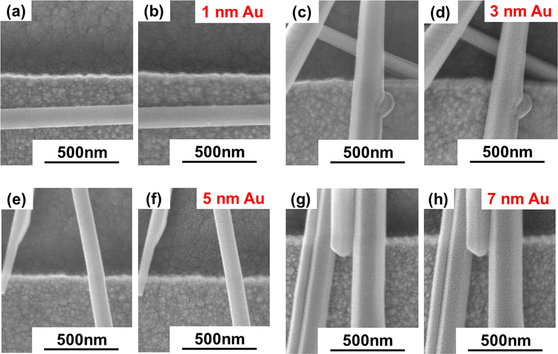
A first morphological study of the gold nanoparticle layer was performed by SEM imaging. Nominal thicknesses of 


 and
and  of catalyst layer on the ZnO NW surface, as measured by a crystal quartz microbalance, were deposited and thereafter tested in the gas sensing setup. The crystal quartz microbalance for Au nanoparticle layer thicknesses meassurements was calibrated with x-ray reflectometry (XRR) data. The respective SEM images (inLens, 5 kV) of the sensor surface before and after sputtering are displayed in figure 3 for Au thicknesses of 1 nm, 3 nm, 5 nm and 7 nm and figures S3(a)–(b) for 10 nm. In the SEM images, the pristine ZnO NW surface appears to be very smooth in comparison to the insulating sensor substrate. After successful deposition of the catalyst at room temperature without additional annealing, an increased roughness of the ZnO NW surface appears to be visible. The corresponding image contrast becomes more pronounced with increasing Au layer thickness. We conclude that the surface functionalization with Au results in a discontinuous nanoparticle layer with Au islands and in-between gaps (indicating uncovered substrate regions). For Au catalyst layer thickness of 10 nm we still observe remaining gap regions. However, the I(V)-curve of a sensor with a surface functionalization of 10 nm clearly shows ohmic behaviour in contrast to a surface functionalisation of 7 nm and less which exhibits Schottky contact behaviour (figures S3(c)–(d)). Evaluating the resistance of sensors before RNWs(i) and after RNWs(Au) their functionalisation reveals an electrical resistance decrease by more than 4 orders of magnitude for the 10 nm Au sensors (table S1). Therefore, we conclude that the sensor with 10 nm Au layer thickness is covered by a Au layer showing percolation behaviour (i.e. a continuous current path through the metallic Au connecting both electrodes), which acts as an electrical shortcut between the electrodes. The typical H2S sensing mechanism of ZnO NWs, as discussed in section 3.5, is based on conductivity changes in the metal oxide caused by ongoing adsorption and desorption processes on its surface. When a shortcut is present, the highly conductive metal catalyst layer dominates the electrical properties of the sensor. We do not expect a pronounced effect on the metal layer conductivity by H2S adsorption/desorption at room temperature. Hence, samples for which the resistance measurement indicates the existence of such a shortcut behaviour have been excluded from further gas sensing measurements.

Figure 3. SEM micrographs of ZnO NWs before and after sputtering of (a)–(b)  (c)–(d)
  (e)–(f)
  and (g)–(h)
  of Au.
Download figure:
Standard image High-resolution imageFurther analysis of the nanoparticle layer was performed by EDX, as displayed in figures 4 and S4–S9. Figures 4(a) and (d) show single nanowires randomly distributed on a Si substrate without electrodes before and after Au catalyst deposition of  thickness. The SEM images once again display a smooth ZnO NW surface before the sputtering, and an almost closed catalyst layer of Au islands separated by various gaps after the sputtering. The respective EDX spectra were obtained by focusing on a bigger aggregation of ZnO NWs as seen in figures 4(b) and (e). EDX results in table 1 confirm Si, O and Zn contributions for both spectra, and an additional Au contribution only after the sputtering process. No further elements were identified in both spectra. Figures S4–S9 display EDX data of ZnO NWs on sensors without any catalyst functionalization and with 1 nm, 3 nm, 5 nm, 7 nm and 10 nm thick Au functionalization, respectively. The elemental maps include Zn, O, Au and Si contributions. The Au contribution in the elemental maps is clearly visible for sensors with a 3–10 nm thickness. In these samples the largest Au signal is found at the ZnO NW locations which may be a result of Au accumulation at the NWs or enhanced scattering of electrons from the primary beam. The EDX results of each sensor (tables S2–S7) reveal an increasing Au contribution for sensors with increasing Au thickness. Sensors with no functionalisation and with only 1 nm of Au thickness show no clear Au contribution in their spectra and elemental maps.

Figure 4. SEM micrographs and EDX spectra of randomly dispersed ZnO NWs on Si (a)–(c) before and (d)–(f) after sputtering of Au.
Download figure:
Standard image High-resolution imageTable 1. Contribution of oxygen, silicon, zinc and gold in the EDX spectra before Au sputtering (displayed in figure 4(c)) and after sputtering (displayed in figure 4(f)). An additional Au contribution only appears after successful sputtering.
| Element | Weight% (before Au) | Atomic% (before Au) | Weight% (after Au) | Atomic% (after Au) |
|---|---|---|---|---|
| O | 6.81 | 12.51 | 4.79 | 10.37 |
| Si | 76.15 | 79.65 | 64.54 | 79.62 |
| Zn | 17.65 | 7.93 | 13.04 | 6.91 |
| Au | −0.61 | −0.09 | 17.64 | 3.10 |
| Totals | 100.00 | 100.00 |
3.1.3. I(V) characteristic of a non-functionalized gas sensor based on pristine ZnO NWs
The sensors consist of two metallic Ti/Au contacts, which are connected by roughly  pristine ZnO NWs, estimated from scanning electron micrographs. This metal–semiconductor–metal (M–S–M) structure typically shows a distinct non-linear and almost symmetric I(V)-characteristic, which is displayed in figure 5. The electron affinity of n-type ZnO is
  [33], whereas the work function of gold is
  [34, 35]. Hence, the M–S–M structure consists of two Schottky barriers with parallel shunt resistances
  both antiparallel in series with a resistor
  representing the ChemFET formed by the ZnO NWs. By applying a constant bias V to this structure, one Schottky contact operates in forward direction and the other in reverse direction. The bias V is divided into three contributions

with 
 the voltage drop across the forward- and reverse-biased Schottky barrier, respectively, and
  the voltage drop over the ZnO NWs. The equivalent current I flowing through the forward- and reverse-biased Schottky contact
  and
and  as well as the ZnO NWs
  can be described by

with


Here, we assume the ideal case in which both Schottky contacts have an identical Schottky barrier height  and contact area
  According to the thermionic emission theory [36], the saturation current I0 for both contacts is:

where  is the Richardson constant for ZnO with the effective electron mass
  for ZnO.
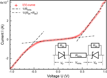
Figure 5. Nonlinear and symmetric I(V)-curve of a typical sensor. The inset displays the equivalent circuit of the M–S–M structure comprising two antiparallel Schottky contacts each with parallel shunt resistor  in series with the resistor
  representing the partially depleted ZnO NWs acting as ChemFET. Linear regression of the measured I(V)-curve allows for an estimation on the total number
  of connected ZnO NWs.
Download figure:
Standard image High-resolution imageThe constant resistance  can be estimated directly by linear regression of the measured I(V)-characteristic in the region
  in the form

On the other hand, the resistance of an ensemble of NWs connected in parallel can be estimated from:

Here,  is the average length of harvested NWs, and
  is their average cross-sectional area. The electrical conductivity of the dispersed NWs
  is calculated by using the donor density
  [37] for ZnO grown in our setup as reported in our earlier works, and the mobility
  for unintentionally doped ZnO at room temperature [38].
As a result, the directly measured resistance is  while the calculated estimation suggests a resistance of
  This difference by a factor of 20 suggests that only a small fraction of ZnO NWs is properly connected to the contact structure. In the presented case, only
  ZnO NWs out of the original estimation seem to contribute to the sensor signal.
3.2. Measurement method and reproducibility of sensors
The main focus of this work lies in the investigation of the effect of the catalytic surface functionalisation of pristine ZnO NW surface by gold on the detection mechanism of H2S sensing with ZnO NWs. In order to separate the role of Au on H2S sensing, the initial pristine ZnO NW sensors in question need comparable electronic and sensor characteristics, e.g. a similar quiescent current level, response  response rate
  signal-to-noise ratio (
 ) and
) and  .
.
Hence, in the first series of H2S sensing measurements the comparability of sensors in the same batch was investigated. Figure 6(a) displays the I(V)-characteristics of two nominally identical gas sensors manufactured from ZnO NWs shown in figure 1. Both sensors were fabricated by dropping  of ZnO NWs freshly dispersed in
  isopropanol onto two pairs of
  long Ti/Au electrodes separated by a
  wide gap. The I(V)-characteristic curves are overall rather similar, and both sensors reach a current level of
  at
at 
The initial H2S sensing behaviour of both sensors was then investigated in a dynamic flushing measurement. Here, the surrounding atmosphere was periodically switched in  intervals between pure oxygen or nitrogen, and
  of H2S diluted in pure nitrogen respectively. As figure 7(b) shows, introducing
  of H2S to both sensors increases the current level linearly by
  and
and  Switching back from diluted H2S to pure oxygen decreases the current mostly back to its initial level
  for both sensors.
Because the H2S is diluted in nitrogen, a current increase between nitrogen and oxygen atmosphere could be expected to partially contribute to the detected signal. To investigate this contribution, during the last intervals both sensors, were flushed with nitrogen instead of oxygen. As discussed in our previous work [39], pure nitrogen does not reset the sensor to the initial current level, which results in an undesirable background current level drift, and makes nitrogen an unsuited candidate for flushing gas. Nonetheless, the inset in figure 7(b) shows that the response rate for 1 ppm of H2S remains rather constant among several flushing intervals and hence is representative for the detection of 1 ppm of H2S. This leads to the conclusion that possible differences in the response of pristine ZnO NWs to pure nitrogen versus pure oxygen can be neglected for the detection of high H2S concentrations in the range of  against oxygen. Initial testing and comparison of the sensors displayed in this work are done in H2S in nitrogen versus oxygen measurements if not mentioned otherwise.
Both sensors start at a quiescent current level of  at
at  in air and an average of
  or
or  at
at  in pure oxygen. The second sensor with the slightly lower current exhibits a lower response rate, which results in an almost identical response for both sensors of
  and
and  for
for  H2S, or a
  of
of  and
and  respectively, as displayed in figure 6. We conclude that identical fabrication leads to sufficient comparability of different samples, what should allow for a straight-forward comparison and interpretation of the possible sensory effects assigned to different Au loadings on ZnO NWs.

Figure 6. (a) I(V)-curve of two nominally identical sensors before and after surface functionalisation. All sensors show typical Schottky contact behaviour in forward direction. Additional Au deposition on the ZnO NW surface increases the measured current. (b) Gas sensing measurements of these sensors before modification. Sensing signals for  H2S versus oxygen and versus nitrogen in
  long intervals. Samples start at the same quiescent current level and show only minimal deviation from each other. The response rate remains constant for both sensors throughout the measurement, and appears to be unaffected by the choice of flushing gas. The inset provides a detailed look at the stable response rate during these 7 continuous detection cycles. It reaches values of
  on average.
Download figure:
Standard image High-resolution image3.3. Gas sensing properties of 1, 3, 5 and 7 nm Au loading on ZnO nanowires
To investigate the catalytic effect of a discontinuous Au nanoparticle layer on the H2S sensing performance of ZnO NWs, multiple series of modified gas sensors with different metal loading on the NW surface were fabricated and compared.
In a first experiment, the previously discussed highly reproducible pristine ZnO NW sensors were loaded with  and
and  of Au catalyst, respectively. After the successful surface functionalisation, a first very noticeable change for both sensors is the increased quiescent current, as displayed in the characteristic I(V)-curves in figure 7(a). Here, the
  sample reached a current of
  at
at  and the
  sample reached a current of
  at
at  compared to the initial value of
  for pristine NWs. This first trend, an increase of the base current level along with an increase of metal particle loading, appears to contradict the effect of Au catalyst loading on metal oxide semiconductors as postulated in literature [40], where surface modification with Au particles is expected to lead to catalytic active oxygen dissociation [40]. When actually more oxygen is adsorbed on the ZnO NW surface, more electrons are trapped on the metal oxide surface, which in turn should result in a thicker non-conductive depletion layer underneath the surface and thus an increase in resistivity of the Au covered ZnO NWs as compared to pristine ZnO NWs. The observed decrease of resistivity can be attributed to two other effects. Before Au deposition, the NWs on our sensors are loosely distributed on top of our contact structure. An additional Au nanoparticle layer possibly improves the quality of the contact between the ZnO NWs and the Ti/Au contact pads. A second more likely explanation is attributed to the morphology of the surface modification itself, and the parallel conduction path via Au islands in a percolation-style situation. It was mentioned that Au nanoparticle films with a too high thickness can even lead to a shortcut between the Ti/Au contact pads. Here, ZnO NWs covered with a
  thick Au layer show already ohmic conduction, which is in accordance to literature where sputtered Au structures show ohmic characteristics above
  film thickness and non-ohmic characteristics below
  [41]. With more Au deposition, the nanoparticles grow in size and undergo a transition from the isolated nucleation stage to lateral Au nano islands growth. The gaps in between the islands start to vanish, and the resistance of the catalyst layer rapidly decreases until the high ohmic current outweighs the catalytic effect of oxygen dissociation.
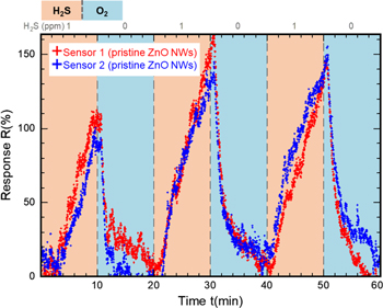
Figure 7. Response of nominally identical sensors with pristine ZnO NWs towards  H2S against oxygen.
Download figure:
Standard image High-resolution imageThe current increase of both modified sensors during exposure to  H2S at
  is shown in figure 8. Because unexpectedly the current limit of our experimental setup was already reached after 3 min, the measurement in the target gas interval had to be interrupted. The
  and the
  sensor started at a quiescent current of
  and
and  in pure oxygen atmosphere, and reached a current of
  and
and  after 3 min exposure to H2S. During the first 1.5 min of the target gas interval, the previous flushing gas atmosphere is completely replaced. First, the quiescent current is kept, and then is followed by a linear current increase with approximately
  and
and  for sensor 1 and sensors 2, respectively. Seemingly, the detection signal never saturates during the
  long exposure to
  H2S at
  which leads to an approximate response of
  and
and  and a
and a  of
of  and
and  of H2S in nitrogen for sensors 1 and 2, respectively. These values only represent a rough estimate and hence no error margins are quoted. Apparently, additional surface functionalisation of pristine ZnO NWs on the on hand leads to a quiescent current increase due to the additional conduction path via the Au nanoparticle layer, and on the other hand the ZnO NWs now show a response rate significantly enhanced by three orders of magnitude as compared to before functionalisation. The
  noise for both sensors appears to be in the same order of magnitude and doesn't show clear tendencies related to the different Au loading. However, due to the enhanced response, the resulting
  is largely increased, and the
  drops by two orders of magnitude. These effects appear to be more pronounced for samples with thicker catalyst loading.

Figure 8. Sensing signal for ZnO NWs with  and
and  Au loading. Once
  H2S is introduced to the NWs, the current increases tremendously by up to
  and leads to an
  of
of  The
The  long detection delay during the H2S interval equals the time that it takes for the target gas to travel from the dilution stage to the sensors.
Download figure:
Standard image High-resolution imageIn order to validate the measurement results of this first catalytic surface modification, a second series of H2S sensors was investigated with 
 and
and  thick Au catalyst loadings. Because the
  thickness is hard to control and shows higher variance due to the short sputtering time, two sensors with
  loading were manufactured. The characteristic I(V)-curves of the sensors before loading are presented in figures 9(a)–(b) alongside with the ratio between the quiescent current
  before and
  after surface functionalisation in air for an applied voltage of
  For this series, a lower forward voltage was chosen in order to prevent the sensing signal from exceeding the current limit of our setup. For this series similar trends were found, i.e. the quiescent current level increases after successful Au nanoparticle film functionalisation of any thickness (figure 10(a)). In addition, the response is increased for thicker loading. In this measurement series the sensor with
  loading shows the largest enhancement of the signal when subject to
  of H2S at
  for the first time. However, the catalytic enhancement of the response reduces with every subsequent interval of exposure to H2S, which was especially observed for the
  coverage, and less drastically for
  or 1 nm. This phenomenon strongly suggests a possible contamination of the Au nanoparticle layer by reaction with sulphur from the interaction with H2S molecules (see section 3.5).

Figure 9. (a) I(V)-curves of sensors with pristine ZnO NWs in the range of  and (b) the respective quiescent current increase at
  voltage applied after surface functionalisation. The quiescent current
  after Au deposition is noticeably increased in comparison to the initial quiescent current
Download figure:
Standard image High-resolution image
Figure 10. (a) Response of sensors with modified ZnO NWs towards  H2S and (b) the corresponding theoretically estimated
  A thick catalyst particle layer enhances the response strongly and hence improves the
  The beneficial effect of the catalyst is only temporally active, but decays with ongoing exposure towards H2S.
Download figure:
Standard image High-resolution imageBecause the noise value for all sensors appears to be identical after Au functionalisation, the  is improved through the enhanced response, as shown in figure 10(b). The response for the first measurement interval with
  H2S was determined as

 and
and  and the
  as
as 

 and
and  for
for 
 and
and  Au loading, respectively (table 2). The results support the previously observed trend that a higher catalyst loading improves the H2S sensing ability of ZnO. Here, it appears to be initially possible to improve the H2S sensitivity of ZnO NW strong enough to detect concentrations even in the low ppb region.
Table 2. Direct display of response  and resulting
  for sensors with
 and
and  Au loading. A higher catalyst loading improves the H2S sensing ability of ZnO NWs.
| Sensor | Response 
|

|
|---|---|---|
| 1 (5 nm Au) | 1030 ± 50 | 18 ± 2 |
| 2 (3 nm Au) | 620 ± 50 | 35 ± 4 |
| 3 (1 nm Au) | 480 ± 50 | 66 ± 6 |
| 4 (1 nm Au) | 350 ± 50 | 69 ± 10 |
The rapid contamination process of the catalyst for  Au nanoparticle layer thickness was confirmed by tracking the response and response rate towards
  H2S for all sensors over the duration of 3 weeks, as displayed in figure 11. At first the superior initial sensing ability of the sensor with
  Au loading clearly stands out. However, with increasing number of detection cycles, all four sensors undergo a decrease in response and response rate until after 3 weeks it is impossible to distinguish the sensors solely by their sensing ability towards H2S. After 3 weeks, the sensor response becomes stable and is finally comparable to the initial sensing abilities of pristine ZnO NWs towards gaseous H2S.
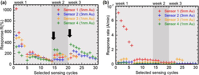
Figure 11. Catalyst lifetime after deposition and detection of  of H2S over the time span of 3 weeks (highlighted with different grey tones) (a) displayed via the response and (b) via the response rate. Black arrows indicate a drifting base current that results from exchanging the sensors in the sensing setup and exposing them to pure air and light. The beneficial effects of surface modified ZnO NWs fades within the first week of H2S exposure.
Download figure:
Standard image High-resolution imageIn addition, comparison of the gas sensing performance of pristine ZnO NWs to H2S with the gas sensing performance to other gases, i.e. methane (CH4) and hydrogen (H2), as shown in figure S10, reveals a clear affinity towards H2S. While the response for 1 ppm H2S is  , the response for high concentrations of 500–10000 ppb of CH4 and H2 stays below 10%. After functionalisation of ZnO NWs with Au the sensor signal shows a response of
  for 1 ppm H2S, whereas no enhanced response is measured for the detection of CH4 and H2 with Au functionalized ZnO NWs. Here, the response towards both reducing gases stays still below 10%.
Summarizing both measurement series, we conclude that ZnO NWs with a thick Au loading led to an overall improved H2S sensing performance, i.e. an enhanced response and a decreased  . The positive enhancements due to the deposition of the Au catalyst increase with increasing thickness, but for 10 nm Au layer thickness electrical short-cut behaviour is found. For the samples investigated in the present study, the best results are found for 7 nm Au layer thickness on ZnO NWs.
3.4. LOD measurements of pristine and modified ZnO NWs
So far, we have compared the detection of H2S with Au modified ZnO NWs to the detection with pristine ZnO NWs. However, H2S was always only diluted in nitrogen. A more realistic scenario, which is closer to medical breath analysis with focus on detection of target gas concentrations in the low ppb range, is a measurement series for H2S diluted in air.
Hence, one sensor with pristine ZnO NWs and for comparison another sensor with surface modified ZnO NWs were prepared for H2S sensing in synthetic air. The ZnO NWs, which were selected for these sensors, were harvested from samples with very homogeneous and particularly thin ( diameter) nanowires. Moreover, the resulting sensors showed very low noise and hence appeared to be very promising for the detection of extremely low H2S concentrations. In order to further enhance the detection signal, the applied voltage was raised to
  and the gas switching intervals were extended from
  to
to  The detection of every concentration was repeated twice before a higher H2S concentration was selected. To make sure that the sensors were exposed towards different H2S concentrations with comparable starting conditions, a
  long flushing interval with pure oxygen was included in between each concentration step.
As shown in figure 12(a), a clearly visible response of  by pristine ZnO NWs was observed for
  of H2S in synthetic air. The response increased linearly with increasing H2S concentrations and led to a theoretically estimated
  of
of  The
The  results of nominally identical ZnO NWs with additional
  Au surface modification are displayed in figure 12(b). For these, an experimentally visible response of
  was measured for
  With a
  of 67 this leads to a theoretically calculated
  of approximately
  In comparison to recently reported works on H2S gas sensors (table 3), Au functionalized ZnO NWs achieve high response and extremely low
  at low working temperature and hence low energy consumption. This outstanding result highlights the tremendous potential of surface modification with metal nanoparticles on metal oxide semiconductors. Here, the surface modification with Au enables the detection of H2S in the ppt—ppb range even in the presence of
  highly oxidative oxygen. The selective catalytic effect of Au towards H2S has been attributed to the strong chemical affinity between gold and sulphur (see section 3.5) [42]. This measurement also demonstrates the deterioration of the catalytic effect of the Au nanoparticle layer functionalisation. Whilst the first exposure to H2S yields a response of
  the response during the second interval for H2S diluted in air already decreases to
  This observation underlines the need for a better understanding of stability and degradation mechanisms in the Au functionalized sensors.

Figure 12. H2S sensing of ppb concentrations of H2S diluted in synthetic air with (a) pristine ZnO NWs and (b) Au loaded nanowires. Additional surface modifications enables the detection of H2S concentrations in the low ppb range. Here, the experimentally obtained and theoretically calculated  for both sensors is displayed.
Download figure:
Standard image High-resolution imageTable 3. Comparison of sensing performance towards H2S presented in this work and recent sensors reported in literature. Response reported by other works is either defined similar to  or simply similar to
  with
with  being the saturated sensor signal in target gas atmosphere.
| Material | Working temperature (°C) | Concentration (ppm) | Response | Response/Recovery time (s) | Detection limit (ppb) | References |
|---|---|---|---|---|---|---|
| Pd-WO3 | 190 | 25 | 242 | 1/x | 2500 | [43] |
| RGO-SnO2 nanofibers | 200 | 5 | 34 | 120/100 | 1000 | [44] |
| PANI/ZnO microdiscs | RT | 0.1 | 3.2 % | 63/12 | 100 | [45] |
| ZnO nanoparticles | RT | 0.75 | 73.3 % | 93/90 | 30 | [46] |
| ZnO hollow tubule | 217 | 10 | 85.04 | 61/59 | 10 | [47] |
| ZnO NWs (branched) | 300 | 0.005 | 3 % | 258/x | 3 | [48] |
| mesoporous SnO2 | 92 | 100 | 107 | 64/56 | 0.5 | [49] |
| ZnO NWs | RT | 1 | x | x | 50 | Previous work [39] |
| Au/ZnO NWs | RT | 0.01 | 80 % | x | 0.5 | This work |
3.5. General discussion
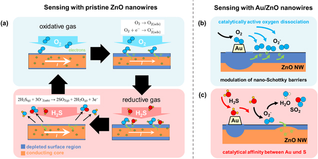
The gas sensing mechanism of ZnO is based on the continuous adsorption and desorption of molecules on the metal oxide surface. ZnO is inherently a n-type metal oxide semiconductor. Deep acceptor-like surface states on the ZnO NWs lead to an accumulation of negative charges and finally to the formation of a permanent thin surface depletion layer with low carrier density, while the nanowire core remains n-type conducting.
When oxygen is interacting with the ZnO NW surface, it will ionosorb in molecular (O2
−) and atomic (O−, O2−) form on unoccupied chemisorption sites by trapping electrons from the conducting core of the ZnO NW to its surface [50] (figure 13(a)). This charge transfer leads to an accumulation of negative charges on the surface, and thus an upward band bending at the ZnO NW surface and hence an increase of the thickness of the surface depletion region relative to the conducting nanowire core. The resistance of the NWs increases, and the measured current at constant voltage decreases accordingly. For temperatures below  the molecular form of oxygen dominates, and the chemisorption of oxygen can be described as [50]:


Figure 13. Sensing mechanism of (a) pristine ZnO NWs and (b-c) Au functionalized ZnO NWs. An additional depletion region resulting from the formation of nano-Schottky barriers between Au and ZnO and the affinity for catalytic dissociation of H2S molecules via active adsorption sites on the Au surface lead to a tremendous improvement of the gas sensing abilities of ZnO NWs.
Download figure:
Standard image High-resolution image
When the reducing gas H2S is introduced to the electron depleted ZnO NW surface, the previously adsorbed oxygen species will interact with the target gas, which leads to the desorption of oxygen by charge transfer, as described in [51, 52]:

By finally forming H2O and SO2, the chemisorbed oxygen is removed and trapped electrons are released back into the conducting NW core. As a result, the surface band bending is relaxed and the width of the depletion region decreases. This is the sensing mechanism observed for pristine ZnO surfaces.
Once Au is dispersed on the ZnO NW surface, the catalytic activity of Au will strongly influence the sensing mechanism. Because the work function of Au [35] is larger than the work function of ZnO [53], electrons will transfer from the metal oxide to the noble metal [42]. These nano-Schottky barriers lead to the formation of an additional depletion region in the contact area between ZnO and Au (figure 13(b)). An additional nanoscopic initial depletion region just underneath the Au islands, which will be modulated by oxygen and H2S adsorption, leads to an enhanced resistance change within the nanowires in comparison to the pristine ZnO NW case. This enhanced modulation depth can easily be observed via the increased response.
Another very beneficial effect of Au modification of the ZnO NW surface is the catalytically activated dissociation of gas molecules. Due to the strong catalytic affinity between Au and sulphur [54], Au acts as a highly active adsorption site for gaseous H2S. H2S interacts rather selectively with the Au nanoparticles and transfers to the ZnO NW surface (figure 13(c)). This spill-over effect results in a quantitatively increased interaction of H2S with adsorbed molecular oxygen, as well as the increased rate at which the release of previously trapped electrons into the conduction band of ZnO occurs.
A similar effect is expected for the catalytic dissociation of oxygen [40], although this is difficult to verify in our measurements due to the enhanced quiescent current in the Au/ZnO structures and the preferential interaction of H2S with Au/ZnO instead of oxygen with Au/ZnO for H2S diluted in synthetic air. As was mentioned before, this is contradicting an enhanced oxygen dissociation.
While both effects, the additional depletion region and the catalytic adsorption of H2S, tremendously enhance the sensing ability of Au/ZnO NWs towards H2S, the affinity between Au and sulphur most likely leads to an irreversible contamination of the catalyst at room temperature. Considering the strong affinity of both elements, a reactive interaction is rather likely [42, 55, 56]:

H2S adsorbed on Au reacts to Au-SH and Au-S type species, which results in the Au nanoparticle layer being covered by a sulphide shell over time [42]. With ongoing exposure to H2S, the Au particles lose their catalytic adsorption activity and the spill-over effect vanishes. In the present work, this behaviour was observed for all Au/ZnO samples. As an outlook, we want to perform a detailed investigation of the surface composition of Au functionalized ZnO NWs before and after H2S detection with additional x-ray photoelectron spectroscopy (XPS) data.
4. Conclusion
High quality ZnO nanowires were successfully grown on Si (100) by high temperature CVD growth using the VLS method. These nanowires were harvested, and in a second step their surface was functionalized over a wide thickness range of discontinuous gold nanoparticle films. Based on the fabrication of comparable gas sensors, the beneficial effect of Au loading of 


 and
and  thickness on a pristine ZnO NW surface was systematically compared. Already
  of Au was enough to increase the channel current and enhance both the response and the response rate of functionalized sensors. A thicker Au loading was causing a stronger enhancement of the overall gas sensing related properties of ZnO. Thicker Au loading leads to improved sensor response for the detection of H2S, but a too thick film leads to a short circuit and high sensor current without reaction to H2S. In the present study, we find the strongest enhancement of the interaction between H2S and ZnO, or H2S and Au, respectively, for 7 nm Au loading which is mainly attributed to the strong chemical interaction between gold and sulphur as proposed in literature. So far, this beneficial adsorption of H2S molecules on the Au nanoparticle layer and the ZnO NW surface lead to an ongoing and rapid contamination of the catalyst. The initial large enhancement of the sensitivity is lost with ongoing H2S exposure, until only the sensing properties of pristine ZnO NWs remained. However, the extreme magnitude of the catalytic enhancement allowed for a temporary detection of exceptionally low concentrations of H2S diluted in synthetic air. Here, sensing of outstandingly low concentrations of
  and theoretically estimated
  of H2S were achieved. In future works we will aim on clarifying the degradation mechanism of the Au catalyst on the ZnO NW surface during H2S detection.
Acknowledgments
The authors thank Dr H Schieferdecker for the dedicated technical support in the measurement setup and A Minkow for the EDX data. Moreover, we thank the 'DFG-Deutsche Forschungsgemeinschaft' for funding this project under contract number 398819137.
Data availability statement
The data that support the findings of this study are available upon reasonable request from the authors.