
Abstract
A wafer-scale fabrication method for isolated silicon quantum dots (Si QDs) using standard CMOS technology is presented. Reactive ion etching was performed on the device layer of a silicon-on-insulator wafer, creating nano-sized silicon islands. Subsequently, the wafer was annealed at 1100 °C for 1 h in an atmosphere of 5% H2 in Ar, forming a thin oxide passivating layer due to trace amounts of oxygen. Isolated Si QDs covering large areas (∼mm2) were revealed by photoluminescence (PL) measurements. The emission energies of such Si QDs can span over a broad range, from 1.3 to 2.0 eV and each dot is typically characterized by a single emission line at low temperatures. Most of the Si QDs exhibited a high degree of linear polarization along Si crystallographic directions [ ] and [
 ]. In addition, system resolution-limited (250 μeV) PL linewidths (full width at half maximum) were measured for several Si QDs at 10 K, with no clear correlation between emission energy and polarization. The initial part of PL decays was measured at room temperature for such oxide-embedded Si QDs, approximately several microseconds long. By providing direct access to a broad size range of isolated Si QDs on a wafer, this technique paves the way for the future fabrication of photonic structures with Si QDs, which can potentially be used as single-photon sources with a long coherence length.
Export citation and abstract BibTeX RIS

Original content from this work may be used under the terms of the Creative Commons Attribution 4.0 license. Any further distribution of this work must maintain attribution to the author(s) and the title of the work, journal citation and DOI.
1. Introduction
As the second most abundant element in the earth's crust (after oxygen), silicon, an indirect bandgap semiconductor, has in fact dominated the semiconductor industry. Beside its high abundance, Si is stable, virtually non-toxic as well as biocompatible. However, as a light emitter, bulk silicon is not a good performer because of its indirect bandgap, which has eventually hindered active components for Si photonics. Inspired by the discovery of visible (red) photoluminescence (PL) in porous Si at room temperature in 1990 [1], in the past 30 years a number of researchers have put tremendous effort in the study of nano-sized silicon, attempting to increase the luminescence efficiency. Indeed, when the physical dimension of a silicon crystal is smaller than the exciton Bohr radius, various favorable and unique characteristics based on quantum confinement effects such as the quantization of the energy levels and the breakdown of the momentum conservation rule, start to appear [2–4]. In particular, the breakdown of k-conservation rule in Si nanocrystals [3] opens a new channel for the radiative recombination of carriers (called a 'quasi-direct' transition) and the probability of the radiative recombination increases compared to the bulk material [5]. More importantly, carrier diffusion to non-radiative recombination centers, as available in bulk material, is suppressed [6]. In addition, the optical properties of the nano-sized silicon can be tuned by regulating its size, shape and surface [7, 8]. To date, silicon quantum dots (Si QDs) have become a promising material with a wide variety of applications in opto-electronic devices [9, 10], solar cells [11, 12] and biological fluorescence imaging [13, 14]. Regarding the fabrication of Si QDs, a wide spectrum of approaches has been reported in the past three decades, which can be divided into two categories: top-down and bottom-up (chemical synthesis).
In principle, bottom-up methods may use silicon-containing molecules as precursors to prepare highly crystalline Si QDs, relying on the self-assembly process [15]. A well-established procedure uses hydrogen silsesquioxane (HSQ) as a sub-stoichiometric precursor. In the furnace the solid ceramics is usually heated up to 1100 °C for 1 h under a reducing atmosphere of 5% H2 in 95% Ar. Given the thermodynamic instability of this Si-suboxide [16], Si QDs of different sizes can form in the matrix of SiO2. Hydrofluoric acid (HF) is subsequently used to etch the solid and liberate the hydride surface-terminated Si QDs into solution [17, 18]. Nevertheless, the high cost of HSQ together with the low mass yield (∼10%) limits the mass production.
In contrast with bottom-up approaches, top-down methods are essentially based on the breakdown of large Si pieces into nanoparticles. The most popular method for preparing Si QDs is via etching of bulk silicon. HF and H2O2 were firstly used to electrochemically etch porous silicon into nanometer-sized structure containing hydrogen-terminated Si QDs [19]. With the addition of a unique electrolytic catalyst in combination with current density, a new synthesis method was developed, allowing fine control over particle size (1–4 nm) [20]. Among other methods, mechanical grinding, a conventional method of manufacturing nanomaterials, was also used to directly break down large-sized silicon into small Si nanocrystals.
Chemical synthesis methods aim at mass fabrication of such nanoparticles for various light-conversion applications. Fabrication of isolated Si QDs on wafers, using CMOS-compatible technology, may possibly expand the application area toward quantum technology. In particular, single photon sources have been successfully demonstrated using epitaxially grown III–V quantum dots [21, 22] and, more recently, defects in 2D materials [23]. In this respect long exciton lifetime in Si nanocrystal quantum dots may be translated into a long coherence length (several kilometers) of the emitted photons for quantum technology [24]. While spin coherence in lateral Si QDs has been widely investigated [25, 26], coherence of photon states for quantum technologies have been so far limited to direct bandgap semiconductor QDs (tens of centimeters) [27].
Previously, electron beam induced deposition lithography and subsequent plasma etching was utilized to produce sub-10 nm Si QDs from a thin silicon-on-insulator (SOI) substrate [28]. A rapid oxidation in pure oxygen at 900 °C was performed to passivate the surface of the Si QDs with oxygen. With this strategy only a small area (∼μm2) of Si QDs could be obtained and the emission linewidth was inferior to short-ligand passivated nanocrystals [29].
Herein, a lithography-free wafer-scale fabrication of isolated Si QDs with improved passivation for enhanced optical performance is presented. Oxide-passivated Si QDs are randomly formed from the device layer of an SOI wafer, which has been thinned by reactive ion etching (RIE) and passivated by a high-temperature (1100 °C) thermal oxidation. The surface density of the Si QDs is low enough for far-field single-dot optical detection. We report strongly polarized emission predominantly in two crystallographic directions, which makes possible polarization-selected resonant excitation in single Si QDs. As demonstrated previously for direct bandgap quantum dots this is an important pre-requisite for achieving transform-limited linewidth characteristics [30]. Narrower linewidths for oxide passivated Si QDs are recorded in a broad temperature range, attributed to better quality of the passivating shell, which was formed at an elevated temperature. Covering full area of wafers with such nanocrystals will also facilitate subsequent fabrication of photonic structures, such as resonant cavities/mirrors or waveguides, for more efficient extraction of individual photons [31–33].
2. Experimental methods
In this work, an SOI wafer with a 50 nm thick device layer and a 150 nm thick buried oxide (BOX) layer was used. To fabricate Si QDs it was diced into ∼1 cm2 chips and exposed to RIE for thinning down of the device layer. Silicon nano-islands were formed and the passivation of the Si core was achieved by thermal annealing in a trace oxygen atmosphere at high temperature (1100 °C). A schematic representation of the fabrication process is presented in figure 1.
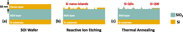
Figure 1. Schematic representation of the fabrication process. (a) The process started with an SOI wafer with ∼50 nm device layer. (b) The device layer is non-uniformly etched down by the reactive ion etching, leading to the formation of Si nano-islands. (c) After thermal annealing Si QDs and Si QWs are formed, passivated by a SiO2 shell.
Download figure:
Standard image High-resolution image2.1. Reactive ion etching (RIE)
In the vacuum chamber of the RIE system, HBr (40 mlpm), Cl2 (15 mlpm) and O2 (10 mlpm) gases were injected from the top. A plasma was generated at a pressure of 40 mTorr at room temperature by a radio frequency electromagnetic field, oscillating at a frequency of 13.5 MHz and applied at 300 W. The reactive ions were energized and accelerated by a DC bias voltage toward the SOI wafer. The device layer was thinned down at a relatively constant rate, ∼4 nm s−1, which is a calibrated parameter of the RIE machine (Applied Materials Precision 5000 Mark II). Thus, the etching time could be chosen so as to roughly estimate the thickness of the remaining silicon layer. The etching process goes from a high rate at the edge of the wafer to a low rate toward the center of the wafer. This is due to a high Reynolds number leading to a slight turbulence at the edge of the wafer that propagates toward the center. Hence the reaction mixture and energy of the gases that etch silicon varies across the wafer, contributing to intrinsic non-uniformity in the etching. In contrast with the typically isotropic profiles of wet chemical etching, the key attribute of RIE technology is its directional etching capability and non-uniformity, producing anisotropic surfaces. As a result, nano-islands of silicon are formed after certain processing time [34]. We rely on this feature of RIE to fabricate isolated Si QDs across large areas.
2.2. Thermal annealing
In this work, the standard annealing furnace was purged with N2 flow and then pre-heated only with the ceramic holder at the preset temperature, aiming at wiping out the remaining gas and burning off solid impurities, respectively. After these pretreatments, only trace amount of O2 remained in the system. In a slightly reducing atmosphere of 5% H2 in Argon, the sample was thermally annealed at 1100 °C for 1 h. This reducing atmosphere, with suppressed oxygen content, slowed down the oxidation rate of silicon nano-islands and protected them from being fully oxidized. Indeed the oxidization rate of a plane silicon interface at this temperature can be approximately 100 nm h−1 [35]. Here the local temperature of the formed oxide shell was close to its glass transition temperature (1200 °C). At such elevated temperature the quality of the oxide shell is substantially better than from a self-limiting oxidation at 900 °C, used previously, where strain builds up resulting in trap sites [36]. With the reduction of the Si core by thermal annealing, oxide-passivated Si QDs were formed on the top of the BOX layer. This process could be monitored using PL images of the chips under UV excitation before and after annealing, as shown in figure 2(b). The high bandgap of the oxide shell confined the carriers to the Si core and, thus, a core/shell nanoparticle system was established. Apart from the confinement, the oxide shell can also shield carriers from the outer surface. Thus, oxide-passivated Si QDs tend to exhibit very stable properties [2].
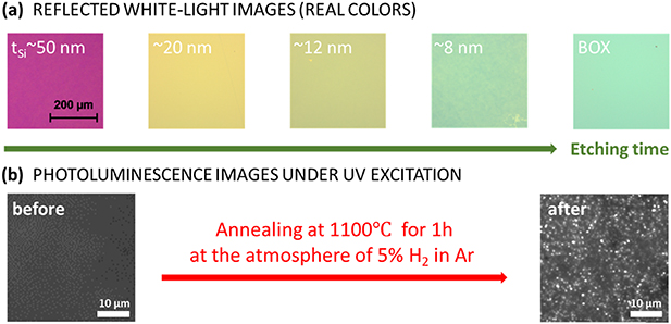
Figure 2. (a) Reflected WL images in bright field (BF) showing the etching of the Si layer, recorded with a color camera. The color from the thin-film interference indicates different Si layer thickness (tSi), as estimated from the etching rate. (b) PL images under 405 nm excitation before (left) and after (right) the annealing process, recorded with a cooled CCD camera.
Download figure:
Standard image High-resolution image2.3. PL characterization
The micro-photoluminescence setup was used to address the optical properties of the fabricated Si QDs on a single particle level. The excitation beam (a λexc = 405 nm diode laser) was directed to the sample either through the lens of the microscope (bright-field configuration) or from outside (darkfield configuration). The emission light from the sample was collected by an inverted optical microscope (Zeiss Axio Observer Z1) with a 100× objective lens (Nikon, NA = 0.73 and field-of-view 150 μm). It was then filtered from the excitation light using a series of 442 and 561 nm long-pass filters (Semrock) and captured by a color camera (Zeiss AxionCam) at the right port of the microscope. On the left port, a spectrometer (Andor SR500) with two different gratings of spectral resolution 0.9 and 0.08 nm (∼250 μeV in the nanocrystal emission range) was connected to a thermoelectrically-cooled EMCCD camera (Andor iXon3 888). For low-temperature PL characterization the sample was placed on the cold finger of a liquid helium flow cryostat (Oxford Microstat) under vacuum, which was then mounted on the microscope sample stage. For time-resolved measurements, a pulsed laser beam was applied with ∼50% duty cycle and a variable repetition rate in the ∼kHz range specific for the decay measurement of each single Si QD. For polarization-resolved studies a rotational linear polarizer was inserted after the objective lenses. To get an acceptable signal-to-noise ratio each spectrum acquisition lasted at least 30 s. All spectra were corrected with the system response curve.
3. Results and discussions
To track RIE process, in figure 2(a) the reflected white-light (WL) images in bright field with elapsed etching time are shown in real colors. The color is closely related to the thickness of the residual silicon layer. Note that the thickness of the device layer is not obtained by precision measurements but roughly estimated from the constant etching rate at a certain etching time. With a close look at the WL images corresponding to ∼8 nm thickness, it is obvious that the surface is not uniform. It is reflected in subtle color difference across the chip. This originates from the non-uniformity of the dry etching process with random variations at the nanometer scale. Formation of such nano-islands of uneven size on top of an SOI wafer as a result of RIE was observed previously by electron and atomic force microscope [34, 37]. When we select the etching time corresponding to the ∼8 nm thick device layer, the size of silicon islands reaches a minimum. Afterwards, no more thin-film interference colors from the Si nano-islands can be distinguished, corresponding to the complete removal of the top Si layer.
As shown in figure 2(b), no PL can be seen immediately after the plasma etching. Subsequently, the annealing process is aimed at further decreasing the dimensions of the silicon islands and passivating their surfaces. The annealing temperature, the time length and the ambient atmosphere are the main factors influencing the oxidation conditions. After several repeated attempts, when the sample was annealed at 1100 °C for an hour at atmosphere of 5% H2 in Ar, the PL of Si nanostructures containing thousands of isolated luminescent diffraction-limited particles can be detected under UV light excitation. A typical PL image is shown in figure 2(b), revealing many well-separated Si QDs. Estimated from the PL image, the surface density of 'bright' Si QDs is approximately 4.4 × 10⁷ per cm2, sufficiently low to be spatially resolved by far-field optics. This quantity is two orders of magnitude lower than the surface density of Si nano-islands, as deduced from the atomic force microscopy (AFM) image (figure 3(a)). That means it is only a fraction of nano-islands which becomes converted to the sub-10 nm well-passivated luminescent QDs by thermal annealing. Remaining fractions are 'dark' Si QDs, large QDs/QWs and fully oxidized nano-islands.
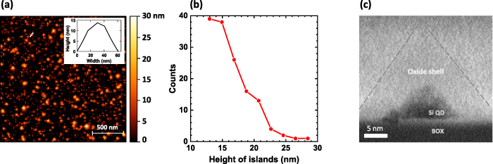
Figure 3. (a) A topographic image of the device layer after the RIE process measured using an atomic force microscope (4.755 nm RMS roughness), with a typical line height profile cut from the white solid line shown in the inset. (b) The height distribution of Si nano-islands in the AFM image. (c) A cross-sectional TEM image of Si QD after the thermal annealing. The dashed lines indicate the profile of the oxide shell.
Download figure:
Standard image High-resolution imageThus, these ultrafine nano-islands can be perceived as the basis underlying the fabrication of Si QDs. In the furnace these silicon islands are gradually consumed by the trace O2, forming well-separated Si/SiO2 QDs. Extensive annealing time completely consumes the top silicon layer. In figure 3(a) an AFM image after RIE process is shown, where isolated nano-islands of different sizes can be clearly resolved. Inset is a typical line height profile. Limited by the size and shape of the AFM tip, the lateral resolution is low (∼20 nm) compared to the vertical resolution (∼0.1 nm). In figure 3(b), the height distribution of Si nano-islands is extracted from the AFM image. Note that only a small fraction (∼1%) of nano-islands correspond to 'bright' Si QDs.
In order to prepare TEM specimens from the annealed Si nano-islands, the sample was firstly deposited with a protective carbon film on the top before the focused ion beam cutting. In figure 3(c), an example of cross-sectional bright field TEM image of an Si QD is shown after thermal annealing, where the lattice fringes of silicon are visible. These nanostructures lie on top of the BOX layer of the SOI wafer. Note that the black dot next to the Si QD without lattice fringes is most likely a contamination particle. At first glance judging from figure 3(c), the Si QD here is not spherical, possessing several facets. A very pale triangle shape surrounding the Si QD can be resolved, appearing to be the oxide shell. This is a convincing evidence of individual Si QD formation from the nano-islands of silicon. Next we turn to the optical characterization of such nanoparticles.
From the color PL image shown in figure 4(a), large areas (∼mm2) covered by the red PL can be seen, albeit no single Si QDs can be resolved in the color camera at this low magnification. This is a clear manifestation of large area fabrication of Si QDs and large-area PL can be detected across the whole wafer surface. Quantitatively it means that literally millions of Si QDs can be fabricated by this technique on a small chip without any lithographical efforts. The emission energies of such Si QDs span over a broad range, from 1.3 to 2.0 eV, as plotted in the low-temperature (10 K) spectra in figure 4(b) for seven individual dots. For each of them, the PL intensities are normalized to their maximum value. Single-dot spectra at 10 K were typically characterized by a single emission line, usually attributed to no-phonon radiative recombination of excitons in the Si core [3]. The variations in the emission energies can be ascribed to the size-dependent quantum confinement effect in silicon. Note that this emission energy range, limited by the detector sensitivity at lower energy, spans the whole emission band normally observed for oxide passivated Si nanocrystals and porous silicon. From theoretical predictions and a large pool of literature [38], the expected size of Si QDs in this work can be estimated from their PL spectra as 2–7 nm. This is consistent with structural characterization shown in figure 3, where the height of core + shell for most of the objects is below 15 nm, and the oxide shell can be at least as thick as the Si core as revealed by the TEM image in figure 3(c).
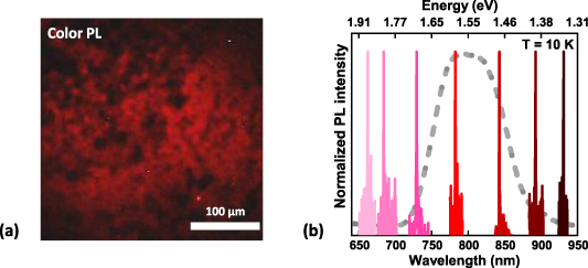
Figure 4. (a) Color PL image (real colors) showing large areas with red-emitting Si QDs and Si QWs. (b) Normalized PL spectra of single Si QDs measured at 10 K. The gray dashed curve is a large-area spectrum indicating the most common wavelength is around 800 nm (corresponding to the QD size of ∼4-5 nm). Excitation was a 405 nm laser in continuous wave mode.
Download figure:
Standard image High-resolution imageTo detect the emission polarization, a polarizer was employed before the emitted light entering the spectrometer and the EMCCD camera. Since only the emission polarization was concerned, the sample was excited by the laser at a fixed incident angle of 45°. While acquiring a 13-frame PL sequence (for each frame the acquisition time is 60 s), each rotation of the polarizer was 15° from one frame to the next. The PL of 90 isolated luminescent nanoparticles as a function of polarization angle was then extracted from the sequence. Note that an (100) SOI wafer was used in this work. Figure 5 shows that most of the Si QDs exhibited a high degree of linear polarization (DLP) along Si crystallographic directions [ ] and [
 ]. Ensemble PL reveals no preferential polarization (not shown), as would be expected from summing up individual curves from figure 5. The same phenomenon of strong emission polarization was previously observed from silicon quantum rods fabricated by electron beam lithography, plasma etching and oxidation, which was attributed to its elongated shape [39]. Herein, it may be due to the crystal orientation dependent etching in RIE and the specific oxidization rate of silicon in terms of different crystallographic planes. As the etching advances, the crystal surface with fast etching rate will appear. It is experimentally proven that
  surfaces experience higher etching rate than other surfaces and eventually pyramidal-shaped silicon islands remain after the RIE etching [40]. This applies to the Si nano-islands in this work as well, which are elongated either along crystallographic direction [
 ] or [
 ] (corresponding to two diagonals of the base of the pyramidal-shaped nano-islands, perpendicular to each other). Also in the one-hour oxidation scheme, with the greatest areal density of Si atoms the crystallographic surfaces
  are oxidized and consumed at a higher rate than that of surfaces
  and
and  [41]. Both of RIE and thermal oxidization give rise to the inevitable elongation or faceting of Si QDs, as shown in figure 3(c). Therefore, PL emission polarization detected here stems from the non-symmetric shape of produced QDs. This effect most likely plays the dominant role in determining the polarization of emission. Apart from polarized light emission, when the spherical symmetry of a quantum dot is broken, faster radiative recombination and even a suppression of Auger recombination can be also expected, contributing to higher light-emitting efficiency [42]. A strong polarization of the emitting state allows resonant excitation, which can reduce extra energy deposited in the system. In direct bandgap quantum dots this allowed to obtain transform-limited luminescence linewidth [30].
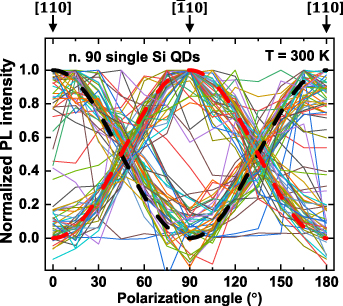
Figure 5. Normalized PL intensity as a function of polarization angle for single Si QDs (continuous lines). Dashed lines indicate linear polarization along silicon [ ] (black) and [
 ] (red) directions. Excitation was orthogonal to those directions.
Download figure:
Standard image High-resolution imageThe PL linewidth is one of the key parameters when judging the quality of a semiconductor quantum dot for light emission. Generally, the linewidth of a quantum dot ensemble is a convolution of the homogeneous broadening and the inhomogeneous broadening. For a single Si QD, the PL spectrum linewidth excludes the effect of the latter. Heisenberg's uncertainty principle sets the limit to the achievable linewidth as reciprocal to the lifetime, also called the transform limit. For Si QDs, given their microsecond long lifetime, this limit yields extremely narrow linewidth in the order of 0.1 neV. In practice, however, the linewidth is homogeneously broadened due to exciton-phonon coupling, exciton fine-structure and spectral diffusion, caused by external charges.
Here, system resolution-limited (250 μeV) PL linewidths (full width at half maximum) were measured for several Si QDs at 10 K, with no clear correlation with emission energy and polarization, as plotted in figure 6(a). Most of these data points lie below the thermal energy at 10 K, demonstrating true quantum dot emission characteristics. Others above the thermal energy are likely to be broadened by spectral diffusion. Additionally, we analyzed the temperature dependence of the average value of the luminescence linewidth for individual Si QDs. For the sake of comparison, in figure 6(b) we included the previous data with respect to oxide passivated Si QDs, which were fabricated by thermal annealing in a pure O2 atmosphere at 900 °C [29]. These two samples would differ only in terms of the quality of the oxide layer. As can be seen, upon decreasing temperature we observed a continuous line narrowing of the luminescence band for both cases whereas the PL linewidths in this work is somewhat narrower than the previous data. Consequently, we attribute the high temperature annealing to the improved quality of the oxide shell. The number of trap sites for charges is possibly reduced, lowering the effect of spectral diffusion.
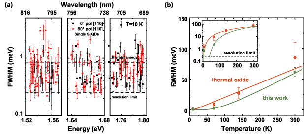
Figure 6. (a) Low-temperature spectral full width at half maximum (FWHM) at three different scans using our high-resolution grating (∼0.08 nm) as a function of emission energy in semi-log scale for Si QDs emitting linearly polarized light along silicon [ ] (black dots) and [
 ] (red triangles) directions. (b) PL linewidths at different temperature from single oxide-embedded Si QDs (1100 °C), comparison with previous data using rapid thermal annealing (900 °C). Inset shows the data in log-scale for clarity.
Download figure:
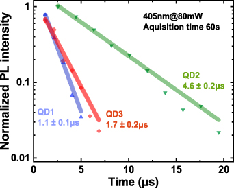
Standard image High-resolution imageTo complete the optical characterization of these newly fabricated Si QDs we performed lifetime measurements on single nanoparticles. In figure 7, the PL decays of three different single Si/SiO2 QDs and their mono-exponential fittings are presented. Because of the rapid trapping (blinking) in oxide-passivated Si QDs at room temperature [36], the decays in such QDs consist of two components: a fast component indicative of the carriers transferring to trap states in the oxide shell and a slow tail due to delayed luminescence as carriers return from resonant traps. Based on this established mechanism, we consider this mono-exponential decay as the first component of the PL decay. Characterization time of this initial part is several microseconds. Although the slow tail cannot be resolved at 300 K, we can estimate that the whole exciton lifetime is in the microsecond range, probably tens to hundreds of microseconds, which is typical for Si QDs [43]. Observed here individual lifetimes are similar to the detected previously from oxide-embedded Si QDs [24].
Figure 7. The initial part of PL decays at room temperature for three different Si QDs and their mono-exponential fits.
Download figure:
Standard image High-resolution image
Last, the repeatability of the process presented in this work was checked by observing no significant variation of the optical properties of Si QDs in a batch of ten different samples diced from the same wafer.
4. Conclusion
In this paper we have reported a two-step fabrication of oxide-passivated Si QDs on top of a thin BOX layer, featuring wafer-scale areas (∼mm2) and low surface density, favorable for single-dot PL measurements. Natural formation of uneven silicon nano-islands covering large areas by the RIE process was the key. High temperature annealing in a reducing atmosphere with trace O2 endows Si QDs with improved quality of the oxide shell. The emission energies of different Si QDs spanned over a broad range, from 1.3 to 2.0 eV measured at 10 K, indicating a broad size distribution originated from the non-uniformity of the dry etching process. Most of the Si QD luminescence exhibited a high DLP along Si crystallographic directions [ ] and [
 ], possibly due to the elongated shape, reflecting etching and oxidation anisotropy. The observed PL linewidths of some individual QDs approached ∼250 μeV at 10 K, thus system-resolution limited. Their PL decays exhibited microsecond time constants, typical for indirect-bandgap QDs. In conclusion, this technique could help the future fabrication of photonic structures with the aim to sharpen the PL linewidth and to increase the signal count rate for the photons from individual Si QDs for quantum photonic applications.
Acknowledgments
This research was supported by the Swedish Research Council (VR) and the China Scholarship Council (CSC).