
Abstract
One of the nanowire (NW) characteristics is its preferred elongation direction. Here, we investigated the impact of Si substrate crystal orientation on the growth direction of GaAs NWs. We first studied the self-catalyzed GaAs NW growth on Si (111) and Si (001) substrates. SEM observations show GaAs NWs on Si (001) are grown along four <111> directions without preference on one or some of them. This non-preferential NW growth on Si (001) is morphologically in contrast to the extensively reported vertical <111> preferred GaAs NW growth on Si (111) substrates. We propose a model based on the initial condition of an ideal Ga droplet formation on Si substrates and the surface free energy calculation which takes into account the dangling bond surface density for different facets. This model provides further understanding of the different preferences in the growth of GaAs NWs along selected <111> directions depending on the Si substrate orientation. To verify the prevalence of the model, NWs were grown on Si (311) substrates. The results are in good agreement with the three-dimensional mapping of surface free energy by our model. This general model can also be applied to predictions of NW preferred growth directions by the vapor-liquid-solid growth mode on other group IV and III–V substrates.
Export citation and abstract BibTeX RIS

Original content from this work may be used under the terms of the Creative Commons Attribution 4.0 license. Any further distribution of this work must maintain attribution to the author(s) and the title of the work, journal citation and DOI.
1. Introduction
The use of nanowire (NW) structures as building blocks for optoelectronics integration and quantum computation has attracted a widespread interest due to their smaller footprint and hence the potential to realize a high density of devices per wafer. With continuous efforts on improving NW growth over the last decade, high-quality III–V NWs have been achieved, mostly on (111) substrates along the vertical growth direction [1–10]. Recently, the bottom-up NW networks deriving from the vertical NWs have been studied as promising candidates for applications in topological quantum computation [11–14]. Among several methods of NW networks formation, NW networks with spatial structures can utilize more spatial volume compared to planar NW networks. Currently, there are three methods to form NW networks with designed spatial structures. The first one is to grow branched NWs, whose successful demonstration is done by a multistep nanocluster-catalyzed vapor-liquid-solid (VLS) process. The difficulties are the controllability of the structural complexity, achieving composition uniformity, and higher yield [15, 16]. The second one is based on the controlled tilting of the NW growth directions by tuning the growth conditions. However, this method is ineffective in producing NW networks. Since to form an interconnect, two adjacent NWs need to be tilted towards each other, which requires a non-rigorous condition allowing multiple growth directions to happen [17, 18]. The diverse and less-controlled growth directions will lower the probability of the formation of NW networks. The third method is based on textured, i.e. patterned, substrates. On such substrates, the walls of patterned trenches face towards each other, which allows NWs with selected growth directions with high unity on both walls to cross and form networks. As a result, the third method has shown optimum reproducibility [19–23]. Therefore, the substrate/facet orientation-determined growth direction of NWs is of significance for the realization of rationally designed NW networks with an increased device density and enhanced spatial complexity. It will benefit from a systematic and exhaustive study of the influence of the Si substrate orientations on the III–V NW growth direction, including the technologically relevant on-axis Si (001) substrates.
For a better understanding of NW growth directions on Si substrates, investigation of the interfaces of droplet/substrate and droplet/NW is crucial. At the interface, two critical factors influence the growth direction of semiconductor NWs by VLS growth mode: (1) The partial wetting and alloying of catalyst droplet with the underlying substrate determines the initial NW growth; (2) The surface free energy of the interface between the droplet and the substrate (or the droplet and the NW) determines the following NW growth as mentioned. There have been several demonstrations on controlling the growth direction of semiconductor NWs by careful tuning of the first factor mentioned above. For instance, UV–ozone and HF etch treatments of the substrates can control the direction of Au-catalyzed GaAs NWs on GaAs (100) substrates by influencing the initial catalyst droplet wetting [24]. The direction and polarity of the Au-catalyzed GaAs NWs on GaAs(111) substrates are affected by the initial droplet conditions with different wetting angles as well [25]. It has also been reported that alloying of the Au-Si droplets during the heating of the substrate, causes roughness or 'etching' of Si substrate beneath the Au catalyst which renders the control of NW growth on Si difficult [26]. The second crucial factor, the surface free energy, usually refers to the total surface free energy, i.e. the energy of unpaired intermolecular bonds, known as the energy of dangling bonds. The dangling bonds occur when the NW side facets and droplet/NW interface are formed, quantification of which and the corresponding surface free energy is not straightforward. In addition, there are further complications, such as surface reconstructions, affecting the total surface free energy. However, it has been reported that the surface free energy at the interface between the NW and the catalyst is generally the dominant component determining the NW growth direction [27].
In this work, self-catalyzed GaAs NWs were grown on differently oriented Si substrates, namely (111), (001) and (311). The microscopic observations followed by a statistical analysis of the data have confirmed the non-preferential growth of NWs in four <111> directions on the Si (001) substrates, and a preferential growth along the vertical <111> direction on the Si (111) substrates. A model is proposed to explain the non-preferential and unique-preference growth along the four <111> directions on Si (001) and Si (111). The model is based on the experimental results obtained by electron microscopy and surface free energy calculations at the droplet/NW interface. The surface free energy calculation is performed by considering the initial Ga droplet formation on the Si substrate and the areal dangling bond density for different facets. Furthermore, a detailed calculation of surface free energy mapping of the droplet/NW interface for NW growth is presented in three dimensions. It predicts selected <111> growth direction of GaAs NWs grown on Si (311) substrates, which further verifies the model. This general model could be applied to predict the NW growth direction on silicon wafers with other orientations.
2. Methods
The surface free energy of the interface between droplet/substrate or droplet/NW determines the following NW growth as mentioned and needs to be calculated. For the total surface free energy calculation, we consider only the surface free energy of the interface facet. As the surface free energy is directly proportional to the number of dangling bonds [28], determination of the areal density of dangling bonds for different facets is key to estimate the total free energy at the droplet/NW or droplet/substrate interface. For that, the atomic structures of different facets are constructed by Vesta software at http://jp-minerals.org/vesta/en/.
Before the determination of dangling bond density for different facets, we need to account for any inconsistencies that may arise when counting the dangling bonds of the atoms on a (111) surface. In this case, (111) surfaces can be approached either from the top or from the bottom as shown in figure 1(a), which represents a single dangling bond surface (SDB) and a triple dangling bond surface (TDB). The (111) surface is commonly observed to be the SDB surface as it is more energetically stable. The surface atoms of the TDB surface have more dangling bonds, leading to much higher surface energy, thus making it unstable. Therefore, in order to reduce the total surface energy by reducing the total number of dangling bonds, these atoms on the TDB surface would rearrange themselves, i.e. reconstruct. However, even after reconstruction, the TDB surface energy is still higher than that of the SDB surface, due to the formation of weaker π-bonds at the TDB surface than those at the SDB surface [29]. Therefore the TDB (111) surface is not considered in most of the reports in the literature [30, 31]. Consequently, to circumvent the dangling bonds inconsistency of the (111) surface as mentioned above, a rough effect of surface reconstruction is taken into consideration. During dangling bonds counting, two kinds of TDB surface are seen. In the first one, three dangling bonds are about to connect with a single atom as shown in figure 1(a), and the other one refers to the opposite side of TDB surface as shown in figure 1(a), where we observe a single atom with one bond connected with an inner atom and three dangling bonds left outwards. The three dangling bonds in both cases for all facets will be counted as only one dangling bond. As this process reduces the total number of dangling bonds, it has the same physical consequence as surface reconstruction. Besides, due to its simplicity, it could be applied to any facets as we have done in the calculations below.
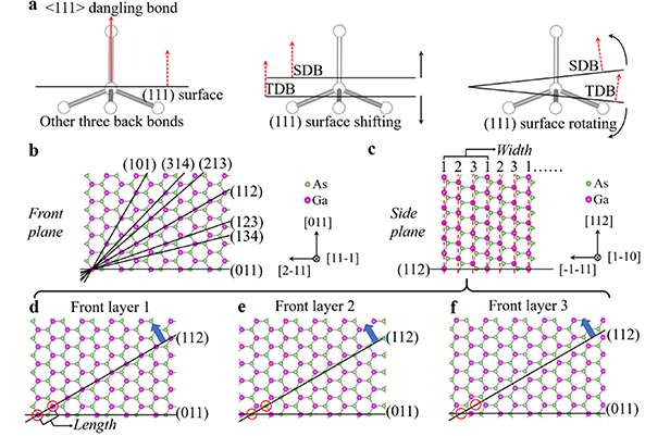
Figure 1. Assumptions and general steps for counting and calculating dangling bonds density. (a) A pyramid of Si atoms represented by grey points with facet (111) passing through the center of the pyramid as well as the body-center of the Si atom. With an extremely small shift or rotation, the broken dangling bonds on the surface of (111) facet will be either one or three corresponding to the SDB surface or the TDB surface. (b) A 'front' plane with observation towards [11−1] direction and upward vector [011], which allows facets (101), (314), (213), (112), (123), (134), and (011) to be seen as lines. (c) The 'side' plane of the same crystal shown in (b), towards [1–10] with an upward vector [112], exhibits a repeated period of three 'front' layers, i.e. the fourth layer is exactly the same as the first 'side' layer. (d)–(f) 'Front' layers 1,2 and 3 from (c). Ga atoms are used as the starting atoms. The blue arrow is in the direction of the (112) facet. The closest Ga atoms in (d) are marked by red circles, and the corresponding locations of these two circles are also marked in (e) and (f). Ga atoms are purple and As atoms are green throughout the Figure. The atoms are treated as points for the facilitation of counting. Note that (b), and (d)–(f) share the same observation indicators.
Download figure:
Standard image High-resolution imageWith the aforementioned assumption, the calculation of areal dangling bonds density is based on the number of dangling bonds on a rectangular surface unit cell for a specific surface/facet. The general steps followed when counting the dangling bonds and then calculating their areal density for any facet are: (1) Finding a front plane with a few facets intersecting perpendicularly. For example, viewing towards an (11–1) front plane with an upward vector [011], (101), (314), (213), (112), (123), (134), and (011) facets can all be seen edge-on as shown in figure 1(b). (2) Finding a side plane perpendicular to the front plane which gives a clear view of an atomic arrangement. For example, in figure 1(c), a view towards a (1–10) side plane with an upward vector of [112] is given, for the same crystalline structure as in figure 1(b), which can be used to determine the areal dangling bond density for all of the facets mentioned above. This way the repeated side unit for, e.g. (112) facet consists of three front layers from 1 to 3 in figure 1(c). (3) To calculate the areal density of the dangling bonds, the counting should be separated for each of the front layers in a repeated side unit. Taking the (112) facet as an example, within the first front plane, red circles mark the two closest Ga atoms, which is the smallest front unit (see figure 1(d)). The same locations are also marked for the second and third front layers in figures 1(e) and (f). As a result, there are four dangling bonds in total per unit area of the (112) facet. The length between the marked circles is  (see figure 1(d)) and the width of the three 'side' layers is
  (see figure 1(c), with
  being the GaAs lattice constant). Thus, the density of dangling bonds of the (112) facet is 4/(
 ) =
) =  . The dangling bond densities of the other facets can be obtained the same way. The advantage of this calculation method is its suitability for even more complicated facets. Please see supplementary information (available online at https://stacks.iop.org/NANO/31/475708/mmedia) Part I for a more complicated example of calculations on facets (012), (138), and (114) and supplementary information Part II for the detailed table of dangling bond densities of facets.
The surface energy can be estimated by multiplying the dangling bond energy and the density of the dangling bonds as expressed by equation (1) [28],

where  is the surface free energy of facet (hkl),
  is the energy of a single dangling bond,
  is the density of atoms on the crystal plane, and
 is the number of dangling bonds per atom on the crystal plane [28]. The density of the dangling bonds for facets presented in the example above is the multiplication of
  and
and  . Here we take the same energy for both bonds, which means the surface energy is proportional to the areal density of the dangling bonds on the crystal plane. It also indicates that we do not consider the polarity effects in our model which will be discussed later.
Despite their simplicity, our calculations show the same trend as the surface free energy calculations which have considered the theoretical strength of the atomic dangling bonds at some specific surfaces in [40] (Red curve in figure 4(a)). Experimentally, the surface energy of discrete facets such as Si (001), (011), (111), (113) and GaAs (110), (001) are measured quantitatively [32–37]. Besides, there were theoretical calculations for semiconductors like Si, GaAs, InAs, AlAs, InP and others mainly on individual low-index facets like (001), (011), (111), (112), (113), as well as the surface energy plot of GaAs along the line from (001) to (110), some of which take surface reconstructions into consideration [38–44]. A summary of comparisons between our calculations and the literature are listed in figure 2.
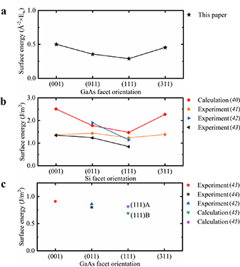
Figure 2. A comparison between our work and other publications. (a) The dangling bond density of GaAs facets (001), (011), (111), and (311) as calculated in this paper. (b) The surface energy for Si facets (001), (011), (111), and (311). (c) The surface energy for GaAs facets (001), (011), and (111).
Download figure:
Standard image High-resolution image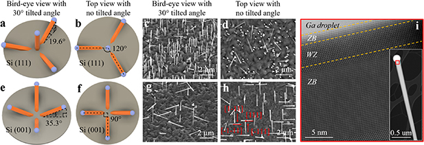
Figure 3. GaAs NWs on on-axis Si (111) and Si (001) substrates. (a)–(b) Schematics drawn based on calculations, showing GaAs NWs on Si (111) substrate with three <111> growth directions having projected angle of 19.6° respecting to the surface of the substrate and 120° azimuth-angle separation between top-view projections as well as the vertical <111> growth direction to the Si (111) substrate (c)–(d) SEM images of GaAs NWs grown on Si (111) substrate from a 30° tilted angle and not tilted views, respectively. (e)–(f) The schematics drawn based on calculations, showing GaAs NWs on Si (001) substrate with four <111> growth directions having an inclined angle of 35.3° to the surface of the substrate and 90° azimuth-angle separation. (g)–(h) SEM images of GaAs NWs grown on on-axis Si (001) substrate from a 30° tilted angle and not tilted views, respectively. Note that the schematics are shown in the same angle of observation as the SEM images and the bird's-eye view is obtained by rotating the SEM sample holder from the position used for top view observation by 30°. (i) High magnification ADF-STEM image of the red square area in the inset shows a WZ structure section below the Ga droplet. The rest of the inspection area has a pure ZB structure. The inset shows the ADF-STEM image of single GaAs NWs grown on Si (001) substrate.
Download figure:
Standard image High-resolution image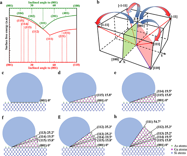
Figure 4. Model for NW growth on Si (001) and surface free energy of different surface facets. (a) The surface free energy of different facets from (100) to (011) is presented by the red line where (111) is the local minimum. Some of the possible transition facets like (115), (114), (113), (112) are marked. The green line represents the surface free energy of from (100) to (001), where (101) is the local minimum. Some of the possible transition facets like (401), (201), (101), (102), and (104) are marked. (b) A demonstration of the four <111> directions with regard to <001> . The red arrows indicate the tilting from (001) growth to two equivalent (111)B directions and the blue arrows indicate the tilting from (001) growth to the other two equivalent (111)B directions. (c)–(h) Growth modes schematics showing the different growth directions that GaAs NWs grown on Si (001) substrates might experience before they turn into <111> direction. Please note that Ga atoms are purple, As atoms are green and Si atoms are blue.
Download figure:
Standard image High-resolution imageSolid source III–V molecular beam epitaxy (MBE) is used for self-catalyzed GaAs NW growth on p-type on-axis Si (001), Si (111), and Si (311) substrates by the VLS growth mode. Ga beam pressure corresponding to a thin film growth rate of 0.6 monolayers per second is used with a V/III flux ratio of 17. The substrates are baked at 200 °C overnight and 600 °C for one hour. Ga source is open for 10 s to form the Ga droplet, then both Ga and As sources are open at the growth temperature of 610 °C for 40 min for all Si substrates. The growth is terminated by stopping both III and V solid sources simultaneously.
Inspections of NWs morphology was done using a Zeiss XB 1540 Scanning Electron Microscope (SEM). TEM imaging and analysis were performed on NWs transferred to holey carbon grids using JEOL 2100 and doubly corrected ARM200F microscopes, both operating at 200 kV.
3. Results and discussions
The possible observation of <111> NWs on Si (111) and Si (001) substrates is considered. The angle between the four available <111> directions of GaAs NWs and the Si (111) substrate surface are indicated in the schematics with bird's-eye view and top view in figures 3(a) and (b). It shows that three of four <111> growth directions have the same projected angle of 19.6° with respect to the substrate surface and 120° azimuth-angle from top-view projections, as well as the vertical <111> growth direction from the Si (111) substrate. However, the SEM images demonstrated that a high percentage of NWs are vertical to the substrate surface, i.e. there is only one preferred <111> direction out of all four <111> directions (see figures 3(c)–(d)). Note that the bird's-eye view is observed by rotating the SEM sample holder from the holder position used for top view observation clockwise by 30° towards <1−10> direction. While this observation is well-known, the preference on the vertical <111> direction has not been studied in detail so far. On the other hand, schematics in figures 3(e)–(f) correspond to the four <111> growth directions on Si (001) with the same projected angle of 35.3° with respect to the substrate surface, and 90° azimuth-angle between them in the top view projections. The SEM images reveal that in contrast to the NWs grown on Si (111), the growth of NWs occurs along the four <111> directions on Si (001) (see figures 3(g)–(h)), also see supplementary information Part III for the confirmation of <111> growth directions on Si (001)). Note that the four <111> directions on Si (001) are marked as left, right, up, and down in figure 3(h). The verification of this non-preferential growth along the four <111> directions of NWs observed on Si (001) still requires further statistical analysis. The Annular Dark Field (ADF)-STEM image in figure 3(i) reveals that the NWs are predominantly of zinc-blende crystal structure with occasional twin defects along the NW. The wurtzite section or zinc-blende/wurtzite polytypism just below the Ga droplet seen here has also been widely reported in other III–V NWs [45, 46], being attributed to the sudden change in the volume of the Ga droplet after finishing the source materials supply in the end of the growth [47–49]. The B-type polarity of NWs on Si (111) and Si (001) is confirmed in supplementary information part IV.
Statistical analysis of the NW growth direction has been carried out on samples grown on both Si (001) and Si (111) substrates. About a thousand NWs have been inspected for each substrate orientation, and the results are summarized in table 1. Similar percentages of NWs were observed along the four <111> directions on Si (001), with 23.2%, 25.5%, 21.7% and 22.1% (in total 92.5%) corresponding to the left, right, up and down directions respectively (as marked in figure 3(h)). It shows clear evidence of the non-preference in growth direction between the four <111> directions when NWs are grown on Si (001). The same statistical analysis carried out on NWs grown on Si (111) shows that there is only one preferred <111> direction, perpendicular to the Si (111) substrate, accounting for 91.3% of the NWs. A small percentage of NWs grown along the other directions can be attributed to the multiple order twinned formation at the initial stage of NW growth [50]. Therefore, it can be concluded that, on Si (111), the growth of NWs along the other three <111> directions is less favorable compared to the main vertical <111> growth direction.
Table 1. The percentages of four major NWs directions with inclined angles of 35.3° to the substrate surface are shown for GaAs NWs grown on Si (001), and that of the major vertical <111> NWs grown on Si (111) as well. For each sample, a thousand of NWs are inspected from SEM images with the same observation setup.
| <111> growth direction for majority of NWs | ||
|---|---|---|
| Substrate | Angle to the surface | Percentage (×100%) |
| (001) | 35.3° [−1−1−1] | 232/1000 |
| 35.3° [−1−1−1] | 255/1000 | |
| 35.3° [−1−1−1] | 217/1000 | |
| 35.3° [−1−1−1] | 221/1000 | |
| (111) | 90° | 913/1000 |
Our general model for determination of the NW growth direction is presented based on (1) an ideal partial wetting and regular shape of catalyst droplet and its alloying with the underlying substrate which determines the initial NW growth direction; (2) The surface free energy of the interface between droplet/substrate or droplet/NW which determines the preference of growth direction for the following NW growth. In Au-catalyzed NW growth, it is relatively difficult to maintain the initial Au droplet in a stable condition at the beginning of the NW growth due to the formation of Au-Si alloy [26]. In contrast, Ga droplets on Si substrate are more stable under heating with less etching and smaller and shallower pinholes [51]. In other words, using Ga-catalyst would have less possibility for pinhole sidewall to nucleate and grow NW on Si substrate. This difference can be explained by the phase diagram of Ga-Si and Au-Si. For example, around 600 °C, the solubility of Si in Ga is negligible, but it is around 16% in Au [52, 53]. Due to its stable liquid form over 30 °C and low reactivity with Si substrate under NW growth temperature, these Ga droplets have partially wetting shapes and flat droplet/substrate interfaces, which reduces the influence of the initial droplet wetting on the growth direction to a minimum [54].
To construct a model predicting NW growth direction on Si (111) and Si (001), we investigated the surface energy of droplet/NW interfaces/facets that may occur during growth. In figure 4(a), the surface free energy calculated using the method described above for different facets from (001) to (110) is shown with the red line. This graph indicates that the (111) facet has the lowest surface free energy. This explains why most of the NWs on (111) substrate only grow along the vertical <111> direction: the first GaAs layer formation on (111) substrate already has the lowest surface free energy in figure 4(a). In order to grow in one of the inclined <111> orientations on the (111) substrate, the interface has to overcome the higher surface free energy barriers. As a consequence, most of the NWs on Si (111) clearly show preferential growth along the vertical <111> direction.
On the other hand, it can be observed that the (001) facet has the highest surface free energy in figure 4(a). If we move from the (001) towards the (111), we can observe how the surface free energy decreases with the inclined angle. Thus, the (115), (114), (113), (112) facets gradually decrease surface energies. To reach a facet with the lowest surface free energy, the formation of (11 n) intermediate facets has to take place. Likewise, the energy curves for the transition from (001) facet to (1–11), (−111), and (−1−11), are the same as the red curve in figure 4(a). Therefore, for NWs grown on Si (001), the tilting towards the lowest surface free energy is equivalent to the four <111> directions. In this case, the four {111} facets have the same (and lowest) surface free energy and consequently, the same probability due to equivalent energy and crystallographic symmetry as shown in figure 4(b).
While this analysis is valid for non-polar semiconductors, e.g. Si or Ge, for the III–V family it needs a slight modification to include the polarity effects. Taking polarity into account, four <111> directions on Si (001) can be differentiated into two <111> B and two <111> A. The two kinds of steps on Si (001) are shown in figure 5(a) which allows two different arrangements for <111> directions of polar semiconductors. Take step 1 as an example, the arrangements of <111> directions on Si (001) are shown for step 1 in figure 5(b). The atomic schematics for the two <111> B (namely, [111]B and [−1−11]B) and the two <111> A ([1−11]A and [111]A) corresponding to step 1 are shown in figures 5(c)–(d). Since we know that (001) facets are the local maximum, and due to the crystallographic symmetry, it leads to the same probability of tilting from growth direction [001] towards [111] and [−1−11] (on step 1, it forms B-polar NW), and the same probability of tilting from [001] towards [−111] and [1–11] (on step 1, it forms A-polar NW). Following the same analysis, we can also show that this conclusion is valid for the situation of step 2 shown in figures 5(e)–(g). Therefore four <111> B or four <111> A directions can be observed on the same Si (001) substrate. In addition, no A-polar NWs are found for the 20 NWs on Si (001). Thus overall, [111] and [−1−11] are equivalent while [−111] and [1–11] are equivalent on Si (001). This is also consistent with the SEM observations and analysis in figures 3(g)–(h). The GaAs NWs marked [111] and [−1−11] are equivalent with similar percentages of 23.2% and 25.5%, respectively. Likewise, the NWs marked [−111] and [1–11] are equivalent with similar percentages of 21.7% and 22.1% out of 1000 NWs, respectively. However, it is noted that there are no necessary relations in terms of growth preference between the neighboring two <111> directions, e.g. [1–11] and [111], in the case of polar semiconductors and it should depend on the distribution of surface steps as well as the difference in the surface energy of A and B facets.
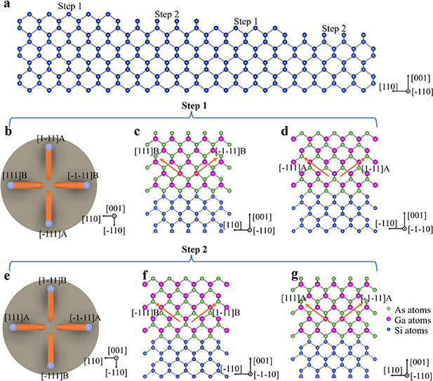
Figure 5. The atomic schematics of four <111> directions on Si (001) with two kinds of steps. (a)–(c) The four available <111> directions for the first kind of step on Si (001) with atomic demonstrations. (d)–(f) The four available <111> directions for the other kind of step on Si (001) with atomic demonstrations.
Download figure:
Standard image High-resolution imageConsequently, in our explanations for GaAs NWs on Si (001), the paths representing the transition from (001) facet to all four {111} facets in figure 4(b) are divided into two pairs (indicated by blue-to-red arrows), as the diagonal <111> directions are equivalent. Taking all these factors into consideration, the NW growth on Si (001) substrate is described by the schematics in figure 4(c). Blue dumbbells correspond to the Ga droplet on top of the Si (001) with [110] projection direction. Here, an As-terminated Si surface is presented as an example (purple atoms at the interface between Si and droplet in figure 4(c)). The formation of GaAs NWs starts at the droplet/substrate interface which is the (001) facet. Since this facet is of high energy, the GaAs NWs will gradually grow inclined facets from (001) to either of (111)B facets, decreasing the total surface free energy of the interface shown in figure 4(a). One of the possible scenarios is shown in figures 4(c)–(h). The formation of GaAs NWs, starting from the substrate (001) surface, evolves through (115), (114), (113), and (112) facets, eventually reaching the (111) facet and continuing the growth along that direction.
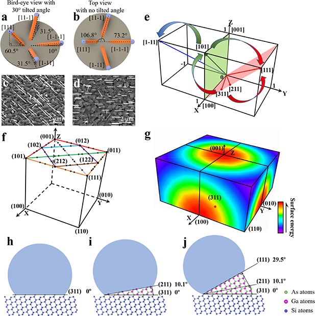
To further verify the model, self-catalyzed GaAs NWs were grown on Si (311) (figures 6(a)–(d)). There are four <111> directions on the Si (311) substrate, forming different angles with the substrate surface. Two of the <111> growth directions have the same 31.5° projected angle to the substrate surface, while the other two have projected angles of 60.5° and 10.0° to the substrate surface, respectively. Azimuth-angle differences between top view projections are 73.2° and 106.8° (figures 6(a)–(b)), see supplementary information Part III for the confirmation of major growth direction on Si (311). Similar to the observations on Si (111), a unique preference among four <111> growth directions is observed (figures 6(c)–(d)). In this case, 932 out of 1000 NWs (93.2%) on Si (311), grow with a projected angle of 60.5° to the substrate. There are very few NWs along the other <111> directions. The crystal quality and polarity of the NWs grown on Si (311) are similar to those of NWs grown on Si (111) and Si (001), which is shown in supplementary information Part IV.
Figure 6. Experimental observations and modeling for NW growth on Si (311). (a)–(b) The schematics drawn based on calculations, showing that NWs at the four <111> growth directions have projected angles of 60.5°, 31.5°, 31.5° and 10° with respect to the surface of the substrate as well as 106.8° and 73.2° azimuth-angle separation between their top-view projections. (c)–(d) SEM images of GaAs NWs grown on Si (311) substrates with a 30° tilt angle and no tilt, respectively. (e) A demonstration of NWs growth directions in a three-dimensional coordinate system, where the red cut-off plane indicates growth directions from [311] to [111] and the green cut-off plane indicates growth direction from [001] [101] and then to [100]. (f) Each of the 55 black bullet points represents a specific surface and are used for the plotting of the top part of the colored 3D surface energy diagram. (g) A detailed surface free energy calculation for growth direction with positive miller index. The magnitude of surface free energy is indicated by a rainbow color system shown at right. (h)–(j) A growth model shows the different growth directions that GaAs NWs grown on Si (311) substrates might experience before they turn into <111> direction. Please note that Ga atoms are purple, As atoms are green and Si atoms are blue.
Download figure:
Standard image High-resolution image
For the corroboration of the model, it is of significance to find out the general regulations behind the preferences in the <111> growth directions. As in this case, most of the NWs shifted preferentially from (311) to (111) growth plane, at a projection angle of 60.5° with respect to Si (311) substrate surface, instead of the other three <111> directions. The NW growth on Si (311) starts on the (311) interface between the Ga droplet and the substrate. To investigate a possible growth plane transition from the initial growth on Si (311), cross-sections written into three-dimensional (3D) coordinate system are shown in figure 6(e). Thus, the red cross-section corresponds to possible growth planes for NWs when shifting from (311), through (211), and finally to (111), marked with red arrows. This transition is supported by the surface free energy calculation (see red line in figure 4(a)). The surface energy transition from (113) to (111) and (311) to (111) are equivalent. This clearly shows that the surface free energy decreases from (311) towards (111) growth plane. On the other hand, for the NW to reach the (1–11) growth plane, it has to pass through one of the growth planes marked on the green cross-section, i.e. from (001) to (101) and to (100). The surface free energy calculated in that plane shows that the lowest surface free energy is at the (101) growth plane, marked with green vector (see green line in figure 4(a)). With these calculations of surface free energy, it seems that there is a chance for the NW growth plane to shift from (311) to (101) then to (1–11). Thus, the construction of a complete surface energy profile is necessary.
To form 3D surface energy mapping by detailed calculations of surface free energy, and confirm the local minimum, we present 10 groups of facets for surface energy of the facets (x y z) with positive integers (x ⩾ 0, y ⩾ 0, z ⩾ 0) in detail. Each group of facets can be seen edge-on with specific observation orientations. Below, when we use (x y z), it translates to (x/z y/z 1) in the coordinate system. For example, the magnitude of surface energy/dangling bond density of facet (113) is represented by a colored point at coordinate (1/3 1/3 1) in the 3D color mapping. We have counted and calculated the dangling bond density of the 55 facets (See figure 6(f)) which are fully listed in supplementary information Part II.
Note that, due to crystallographic symmetry, the broken dangling bond density from facets (001) to (101) and (001) to (011) should be the same, which is also in accordance with our calculation. Therefore, we mark the lines that join (001) to (101) and (001) to (011) both in red. Other symmetric groups of facets are in the same color as well. In total, there are 55 individual facets, which are all highlighted by black bullet points in figure 6(f), used to plot the top part of the colored 3D surface energy diagram. Likewise, the front part and side part can also be constructed, and eventually forms the full-colored 3D surface energy diagram shown in figure 6(g). As a result, the (111) growth plane is the nearest local minimum for the (311) growth plane to reach.
Apart from the surface energy, the growth of the NWs is also influenced and disturbed by factors such as growth temperature and beam flux, which further drives the (311) growth plane through the shortest path to reach the nearest local minimum. In other words, the probability for NWs to grow along <111> with an inclined angle of 60.5° is the highest and it can be predicted to be the dominant growth direction. It is consistent with the results from SEM observations and proves the validity of the proposed model. Although there are few NWs with other growth directions, they can be attributed to non-uniform Ga droplets with different wetting properties. They also might have taken alternative paths to other <111> directions. The atomic model of the transition discussed above is shown in figures 6(h–j). The formation of GaAs NWs starts from the substrate facet (311), then switches to (211) and eventually to the (111) growth plane, which has the lowest local surface free energy and hence the growth continues along the <111> direction afterwards.
It is noted that a most intriguing phenomenon regarding epitaxial semiconductor NWs, which is encountered most frequently and reported very often, is that zinc-blende epitaxial NWs prefer to grow along <111> directions [55, 56], Conventionally, people assume that this phenomenon is attributed to the low surface energy of (111) surface. However, through a careful inspection of the literature, it is found that the current understandings on the surface energy could not lead us to the conclusive elucidation of this phenomenon as the surface energy measurements and calculations are based on merely a limited number of specific facets and directions. Our construction of the 3D surface energy mapping validates (111) surface has lower surface energy compared to all the other facets or at least the facets surrounding the (111) facet which strongly supports this assumption.
Besides, our model could also be generalized to group IV NWs. Consequently, the model agrees with a large portion of results from the literature available on group IV and III–V NWs [27, 46, 57–64]. Although our model can predict the preferred <111> directions among all available <111> directions, there are still some issues outside the scope of the current model. For instance, NW growth along <110> and <100>, whose origins are claimed to be growth-temperature dependent or NW radius dependent, cannot be explained the same way [59, 65, 66]. The possible explanation is that when the diameter of the NW is smaller than a critical value, the side facets surface energy is contributing to the growth direction preference, i.e. the direction along <110> and <100> can be a local minimum of the total surface energy. The low-pressure Si supply is reported to result in a higher rate along <112> direction for Si NWs which is also out of our scope [67]. Additionally, it has been well acknowledged that epitaxial III–V NWs prefer <111> B growth direction. However, the predominance of the B-polar NWs over A-polar NWs cannot be fully understood from our model, which indicates improvements in the details of the calculations might be helpful. Moreover, there may be some other important factors influencing the growth direction than just the surface free energy. For instance, Ga droplet dissipates easier on A-surface, which might suppress the growth of <111> A NW [68]. Further improvements in the calculation of the surface free energy can be achieved by including other factors, e.g. the droplet influence, surface energy of side facets and polarity.
4. Conclusions
In conclusion, we observed preference and non-preference among the four <111> growth directions for the GaAs NWs on Si (111) and Si (001) substrates, respectively. With the help of SEM and TEM measurements, the preferential vertical [111] growth directions on Si (111) and the four non-preferential <111> NW growth directions on Si (001) were observed, leading to a practical model including detailed surface free energy calculations. The model is verified with a more detailed and visualized surface free energy mapping in the three-dimensional coordinate system by the calculation of areal dangling bond density of 55 facets, which explains the most representative observation, namely the <111> growth preference, with proper assumptions. More factors such as the growth conditions, droplet influence, surface energy of side facets, NW morphology and polarity can enhance the accuracy and universality of our model towards understanding the NW growth directions at complex conditions.
Acknowledgments
The authors acknowledge the support of Leverhulme Trust, the UK Engineering and Physical Sciences Research Council–EPSRC (Grant Nos. EP/P000916/1 and EP/P000886/1), and EPSRC National Epitaxy Facility.
Author contribution
X Y and H L guided the overall project. X Y performed material growth. H Z carried out SEM measurements. X Y and H Z analyze the data and H Z and X Y carried out the calculations in this work. H A F and A M S performed TEM measurements. H Z and X Y composed the manuscript and all of the authors contributed to multiple revisions and finalizing of the manuscript.
Competing interest
The authors declare no competing financial interest.