
Abstract
Thermal treatment of carbon nanotubes (CNTs) can significantly improve their mechanical, electrical and thermal properties due to reduced defects and increased crystallinity. In this work we investigate the effect of annealing at 3000 °C of vertically aligned CNT arrays synthesized by chemical vapor deposition (CVD) on graphite. Raman measurements show a drastically reduced amount of defects and, together with transmission electron microscope (TEM) diffraction measurements, an increased average crystallite size of around 50%, which corresponds to a 124% increase in Young's modulus. We also find a tendency for CNTs to bond to each other with van der Waals (vdW) forces, which causes individual CNTs to closely align with each other. This bonding causes a densification effect on the entire CNT array, which appears at temperatures >1000 °C. The densification onset temperature corresponds to the thermal decomposition of oxygen containing functional groups, which otherwise prevents close enough contact for vdW bonding. Finally, the remaining CVD catalyst on the bottom of the CNT array is evaporated during annealing, enabling direct anchoring of the CNTs to the underlying graphite substrate.
Export citation and abstract BibTeX RIS

Original content from this work may be used under the terms of the Creative Commons Attribution 4.0 license. Any further distribution of this work must maintain attribution to the author(s) and the title of the work, journal citation and DOI.
1. Introduction
Owing to their low-dimensional nature, carbon nanomaterials such as graphene and carbon nanotubes (CNTs) have a wide range of interesting properties, both electrical [1], thermal [2–4] and mechanical [5], as well as large specific surface area [6]. Over time, more complicated graphene and CNT based structures have shown potential in various applications [7]. One type of such structure is based on vertically aligned CNTs (VACNTs), which allows for high surface area to volume ratio as well as high and anisotropic electrical and thermal conductivities [8].
In principle, VACNT arrays can form covalent bonds to a graphene or graphite substrate, creating a seamless hybrid material [9–11]. This hybrid structure can be useful for both electrical applications, such as supercapacitor electrodes [10], or thermal applications, as micro heat sinks or thermal interface materials [11, 12]. For optimal performance in these applications, it is crucial to create covalent bonding between the CNT array and the underlying graphene or graphite in order to ensure good thermal or electrical connection.
Arrays of VACNTs are commonly synthesized using chemical vapor deposition (CVD) [13], utilizing a catalyst structure consisting of metal catalyst particles and an immobilizing ceramic barrier layer. This allows for synthesis of well-aligned VACNT arrays up to several millimeters in height [14]. However, CVD methods usually leave the catalyst structure on the bottom of the CNT array, between CNTs and substrate, which in turn severely limits electrical and thermal contact.
Using so-called "odako" growth of CNT arrays, it is possible to create a significantly improved connection between CNT and substrate [15, 16]. This method utilizes a reversed catalyst structure which causes the catalyst to remain on the top of the array instead of the bottom, and has been shown to enable covalent bonding at the CNT/substrate interface [16]. However, the catalyst layer on top causes severe drawbacks. The CNT arrays are shorter by an order of magnitude,  m compared with >500 µm using a conventional catalyst structure. Individual CNTs also have lower quality and are grown in discrete bundles, which results in a non-uniform array [10].
In addition to the poor CNT-substrate connection, the CVD process results in CNTs with a very high degree of defects and impurities [17, 18], including defects in the graphite planes, amorphous carbon on the CNT surface and oxygen containing functional groups [19, 20]. This negatively impacts both electrical [21, 22], thermal [23] and mechanical [18, 24, 25] properties by orders of magnitude. Odaku growth further increase the amount of defects [10] compared to base growth CVD. Post-growth treatment in order to reduce these defects have been investigated using microwaves [26], but so far the improvements are modest. Heat treatment of CNTs is much more effective at removing defects [27–31]. While functional groups can be eliminated at temperatures  C [32, 33] graphitization temperatures (>2500 °C) are required in order to remove defects in the atomic structure and recover the graphite sp2 structure. This improvement in CNT structure in turn increases the electrical conductivity [27], thermal conductivity [34], and Young's modulus [31] of the CNTs. So far heat treatment studies have only been done on small free-standing arrays or randomly aligned samples as most substrates are incompatible with graphitization temperatures.
In this paper, we investigate the effect of heat treatment at 3000 °C on CNT arrays grown on graphite foil. The temperature is above the boiling temperature of both the Al2O3 and Fe in the catalyst structure, causing them to evaporate. This enables heat treatment as a post-growth process to create direct bonding between CNTs and graphite, as an alternative to odaku growth. The heat treatment also increases the crystallinity of both the graphite support and individual CNTs by reducing defects, and therefore dramatically improves their mechanical properties. The heat treatment also increases the inter-tube interaction between adjacent CNTs, causing a densification effect of the CNT array.
2. Methods
The graphite CNT hybrid structure was fabricated using a Joule heating CVD method, using a cold-wall CVD reactor. The graphite substrate consisted of a 25 µm thick pyrolytic graphite sheet (PGS) from Panasonic. A catalyst layer consisting of 10 nm Al2O3 and 1 nm Fe was deposited using e-beam evaporation. A modified version of a commercial cold-wall CVD reactor (Black Magic II, Aixtron) was used for the CVD growth. The PGS was secured between two electrodes within a low-pressure chamber, and localized heating was achieved by running a current through it. The CVD was done in a two-step process, with an annealing step at 500 °C for 3 minutes under a 837 sccm flow of H2 and a subsequent growth stage at 700 °C under a flow of 240 sccm C2H2 in addition to the H2. The CVD method is described in more detail in a previous work [12]. This type of thermal CVD yields an array of vertically aligned metallic multi-walled CNTs (MWCNTs). By varying the length of the growth step, the height of the CNT array could be varied, up to a maximum of >500 µm after 10 minutes.
After CNT growth, the samples were subjected to high-temperature annealing. The samples were placed inside lidded graphite crucibles stacked on top of each other during the process. The temperature was increased to 1000 °C at a heating rate of 5 °C min−1 under a nitrogen flow of 100 sccm. The samples were annealed at 3000 °C under an atmosphere of argon (3000 sccm) at a heating rate of 5 °C min−1, and the samples were kept at this temperature for 1 h.
The crystallinity of the annealed CNT arrays was measured using Raman spectroscopy (Horiba Xplora) with a 638 nm laser (excitation energy of 1.94 eV) on peeled off bundles of the CNT array. The nanostructure of the CNTs was imaged in transmission electron microscope (TEM, FEI Tecnai T20) and the array structure in scanning electron microscope (SEM, Zeiss Supra VP60, operated at 200 kV). Further measurements of the CNT crystallinity were conducted using TEM (JEOL, JEM-2100, operated at 90 kV) by analyses of the diffraction patterns of individual CNTs. The method relies on finding a straight CNT section and measuring the width of diffracted beams. The shape of the diffraction pattern profile was then analysed in the direction along the CNT axis and deconvoluted into Lorentzian and Gaussian contributions. The instrumental broadening was accounted for and we obtained the contributions from the CNT itself and thereby estimated the crystallite size. Further details of this measurement can be found in a previous work [25].
Chemical analysis of the samples before and after heat treatment were conducted using a PHI 5000 C XPS system. The spectra were obtained using monochromatic Al Kα radiation in high resolution mode and the results were shifted to coincide with adventitious carbon at 284.8 eV before interpretation. All relative contributions of the different peaks and their corresponding components were calculated using a Shirley background.
3. Results
3.1. Raman spectroscopy analysis
The crystallinity and amount of defects in the CNTs were investigated using Raman spectroscopy. For MWCNTs, the Raman spectrum is in appearance the same as for graphite provided that the innermost tube has a diameter >2 nm [35]. The features of interest are the D-band at around 1320 cm−1, G-band at around 1580 cm−1 and the 2D overtone of the D-band around 2650 cm−1 [36].
The normalized Raman spectra of annealed (blue) and pristine (red) CNT arrays are shown in figure 1. The most obvious difference is the reduction in D-band peak intensity (ID). The G-band is related to the graphitic structure, while the D-band is induced by disorder within the structure. Thus, the ratio between ID and the G-band peak intensity (IG),  can be used as a measure for the crystallinity of graphitic materials [37]. After annealing,
  decreases from 1.367 to 0.342, which is a clear indication of increased order within the annealed CNTs.
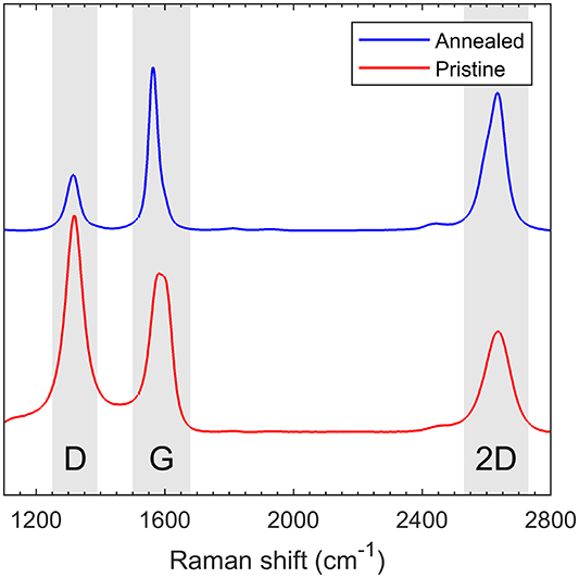
Figure 1. Raman spectra for annealed (blue) and pristine (red) carbon nanotubes measured with a 638 nm laser. The spectra are normalized by the G peak intensity.
Download figure:
Standard image High-resolution imageIn addition to the  ratio, the annealed CNT sample also had an increased ratio between the 2D and G peaks
  as well. This is to be expected, as
  has previously been found to be inversely correlated with
  for MWCNTs [28, 38, 39].
Further investigation reveals a narrowing of the G-band after annealing. The narrowing can be attributed to a reduced contribution of a disorder related D'-peak within the G-band [28]. The G-peak width can be used to extract a quantitative measure of the crystallite size within the CNTs, through an empirical law proposed by Mallet-Ladeira et al [40], which is valid for crystallite sizes between 2 to ∼10 nm:

where ΓG is the half width at half maximum (HWHM) of the G-band peak and La is the average in-plane crystallite size within the CNT. From the data in figure 1 we have ΓG = 34 cm−1 and 17 cm−1, corresponding to a crystallite size La = 5.6 ± 1.4 nm and 9.8 ± 1.9 nm for the pristine and annealed samples respectively. In total, the Raman spectra show a clear and strong indication of a much more graphitic CNT structure after thermal treatment, with a significant reduction in defects and corresponding increase in crystallinity.
3.2. Transmission electron microscopy
Further evidence for CNT crystallinity improvements can be found by TEM as seen in figure 2. Figure 2 (a) shows a representative CNT of an annealed CNT, with straight, well-aligned (002) graphitic planes, indicative of a highly crystalline CNTs with a low degree of defects. This can be compared to the most well-defined CNT found among the pristine CNTs, shown in figure 2 (b). The CNT walls can clearly be seen, but the structure is wavy rather than straight, with numerous breaks indicating defects. Note that this is near the upper limit for as-synthesized CNTs, with a more typical example shown in figure 2 (c), which has an even less defined wall structure and significant amount of amorphous carbon attached.
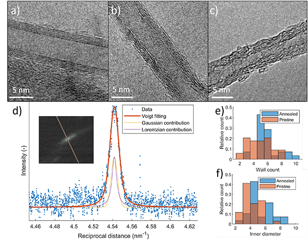
Figure 2. TEM images of annealed and pristine CNTs. (a) Example of an annealed CNT with straight, well defined graphitic walls. (b) Upper end of crystallinity for pristine CNTs, with a looser and wavier structure. (c) Typical pristine CNT, with a high degree of defects and amorphous carbon deposits. (d) Example of TEM diffraction data for a single CNT (blue dots), with fitted Voigt profile (red) with Gaussian (yellow) and Lorentzian (purple) contributions. Inset shows the diffraction pattern of the same CNT. (e), (f) Histogram of wall count and inner diameter respectively, of annealed (blue) and pristine (red) CNTs.
Download figure:
Standard image High-resolution imageIn order to get a quantitative estimate of the increase in crystallinity, we analysed the diffraction pattern of individual CNTs using selective area diffraction (SAD). An example image of the resulting diffraction pattern is shown in figure 2 (d), including the fitting and its Gaussian and Lorentzian contributions. With our set-up we were then able to quantify crystallite sizes in the range of about 2.5 − 70 nm. For the pristine samples we got an estimate of the in-plane crystallite size La = 5.4 ± 2.1 nm, and for the annealed samples obtained an estimate of La = 8.3 ± 2.4 nm. The graphitic parts in the annealed samples shows an even higher crystallinity, with La = 22 ± 2.3 nm. The diffraction pattern displays an oval shaped pattern for non-perpendicular incidence [41], which is indicative of highly crystalline graphene layers with a turbostratic stacking. The La values agree well with the Raman results, considering the margin of errors and the fact that Raman averages over a larger area.
In addition to the crystallinity improvements and obvious structural changes, the annealing had an additional effect of slightly increasing the average diameter and number of walls of the CNTs. Figure 2 (e) and (f) show histograms of the wall count and inner diameter of CNTs based on a survey of 25 CNTs of each kind, randomly chosen among resolvable CNTs. The average inner CNT diameter increased from 4.2 nm to 5.2 nm and the average number of walls from 4.8 to 5.8. For the wall count this change appears to be largely due to elimination of CNTs with  walls. The increased inner diameter is consistent with previous reports of CNT after heat treatment [42]. This increase could be attributed to amorphous carbon present before annealing being incorporated into the CNTs.
On a larger scale additional structural differences are evident. Figure 3 show larger area TEM images of pristine and annealed CNTs. The same characteristics can be ascertained here as well, with more defined walls and less curving for the annealed compared to the pristine CNTs. In particular, the annealed CNTs have formed largely straight regions separated at sharp angles, compared to the continuously meandering as-grown CNTs. A single CNT has been marked in red in each case, illustrating the rounded curvature of the pristine CNTs and sharp angles of annealed CNTs. These kinks are the main type of remaining defects of treated CNTs, and arise from curved CNTs straightening locally, while the global structure remains similar. Andrews et al likewise found that these type of structural defects are not removed by heat treatment [43].

Figure 3. Low magnification TEM view of (a) pristine and (b) annealed CNT structure respectively. In each case a single CNT has been marked (red) to illustrate the sharp angles of annealed CNTs compared to the rounded, flexible structure of pristine CNTs (a).
Download figure:
Standard image High-resolution imageIn conjunction with the straightening of CNT regions, adjacent CNTs tend to bond to each other. This can faintly be seen in figure 3 (b), where several CNTs appear to be aligned and attached to each other for long stretches. In contrast, the pristine CNTs in figure 3 (a) have mostly a clearly visible separation even between adjacent bundled CNTs.
3.3. Inter-CNT bonding
A closer investigation of the aligned CNTs reveals bonding between them, shown in figures 4(a)–(c). Figure 4(a) shows a free single CNT, (b) the boundary between free and bonded (red) region and (c) a completely bonded region. The interlayer spacing in bonded regions appears to be the same as for individual tubes, indicating van der Waals attraction between the tubes. This is illustrated in figure 4(c) where the walls of two CNTs with seven and three walls are marked in red and green respectively. The distance between the outermost wall of the two CNTs is approximately 3.5 Å, similar to single CNT interwall distances [44].
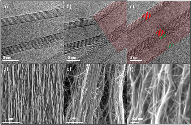
Figure 4. (a)–(c) TEM images of (a) free annealed CNT, (b) boundary between free and bonded region (red) of two CNTs, and (c) bonded region between two CNTs, with seamless graphitic structure joining the two CNTs. The red and green lines indicate the walls of the two bonded CNTs. (d)–(f) Sideview SEM images of CNT arrays. (d) pristine CNT array, (e) annealed CNT array and (f) magnification of annealed array.
Download figure:
Standard image High-resolution imageScanning electron microscope (SEM) images of the CNT array show the same features on a larger scale. The pristine array has distinct, separate, wavy CNTs as seen in figure 4 (d). The annealed CNTs on the other hand, shown in figure 4 (e) at the same magnification, seem to consist largely of fewer but thicker CNTs, which corresponds to multiple bonded CNTs. The trend of straighter CNT segments connected at defined angles can also be ascertained, especially at higher magnification in figure 4 (f).
The spacing between bonded carbon nanotubes indicates van der Waals (vdW) bonding of the same type as interlayer bonding within the CNTs themselves. Tao et al [45] investigated the vdW interaction between CNTs using the van der Waals density functional (vdW-DF) method for nonlocal correlation density functional theory (DFT) [46, 47]. Using the consistent exchange version (vdW-DF-cx) [48], they proposed a binding-energy scaling formula:

where Eb/l is the binding energy per unit length (in Å),  is the number of atoms per unit length and a, b, c and d are fitting parameters obtained by the vdW-DF-cx depending on nanostructure. We used this formula to calculate the average binding energy per unit length for two identical bonded CNTs with outer radius of 5 nm, corresponding to an average annealed CNT. The vdW interaction scales strongly with inverse distance, allowing us to neglect contributions from inner walls of the CNTs. Assuming armchair chirality, a radius of 5 nm corresponds approximately to a (70,70) nanotube. The number of atoms per Å is
  , and the fitting parameters a = 8, b = 250, c = −350 and d = 100 from reference [45]. This yields a binding energy Eb/l = 11.59 eV nm−1 of bonded CNTs. As a rough comparison, the available thermal energy at 3000 °C, is on the order of magnitude of kbT = 0.282 eV per particle, meaning that this adhesion will be stable at very small overlaps.
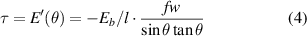
The alignment of the CNT regions can be explained from the information in figure 5. We assume that the binding energy from equation (2) is evenly distributed over an interacting area based on some fraction f of the CNT diameters, marked in red in the schematic interacting CNTs in figure 5. Assuming that the vdW binding is active for parts of the CNT with separation  Å, we get an estimate of f ≈ 0.2 for a 10 nm diameter CNT. Moreover, we also assume that the total binding energy of overlapping CNTs at arbitrary angles is proportional to the overlap in this interacting area. The binding energy of two infinitely long CNTs can now be expressed at an arbitrary interaction angle as
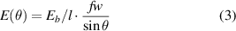
where w is the CNT diameter. This binding energy as function of interaction angle is shown in figure 5 (blue). Note that the infinite CNT length assumption only matters for very small angles. By taking the first derivative of the binding energy in (3) we find an effective torque τ:
Note that since E(θ) is defined as a binding energy, τ is equal to  rather than
  . The torque is also shown in figure 5 (red) as a function of interaction angle. The torque will cause a relative angular acceleration according to
  where I = 1/12 ml2 is the moment of inertia of a cylinder with mass m and length L. Note that equation (4) describes infinitely long CNTs, but this is only relevant at very small angles. The inset in figure 5 shows the solution of the resulting differential equation with the following values: f = 0.2, w = 10 nm,
  kg, L = 1µm and an initial angle θ(0) = 89°. Since the CNTs are mostly vertically aligned in the array, the average initial interaction angle will be relatively small, further facilitating the bonding process. While the specific values are a rough order of magnitude estimation, these calculations show a tendency for bonded CNT regions to align themselves along each other and for bonded regions to grow.
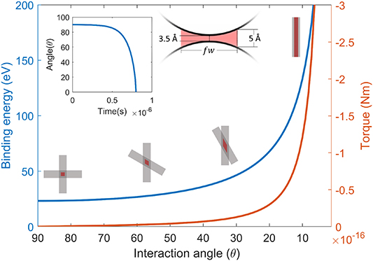
Figure 5. Plot of binding energy (blue) and the resulting effective torque (red) as a function of interaction angle between to bonded CNTs. The figures along the binding energy line depicts CNT angle and the effective interaction area for CNTs at 90°, 60°, 30° and 0° with f = 0.5 for clarity purposes. The interaction area is also shown perpendicular to the CNTs. The inset shows the time evolution of two 1 µm CNT segments with an initial angle of 89°.
Download figure:
Standard image High-resolution image3.4. CNT array densification
On a larger scale, this bonding is responsible for a densification phenomenon of the CNT array, where the array is segregated into densified bundles. Figure 6 (a–c) show a top view of annealed arrays after annealing at 1000 °C, 1200 °C and 3000 °C respectively. At 1000 °C, the CNT array appears essentially pristine, but with minor cracks in the array. At 1200 °C the CNT array has started to break up into smaller bundles, with a densification degree of 40% as measured by the ratio of CNT tip area versus total area. At 3000 °C, the CNT tips only cover 10% of the total area.
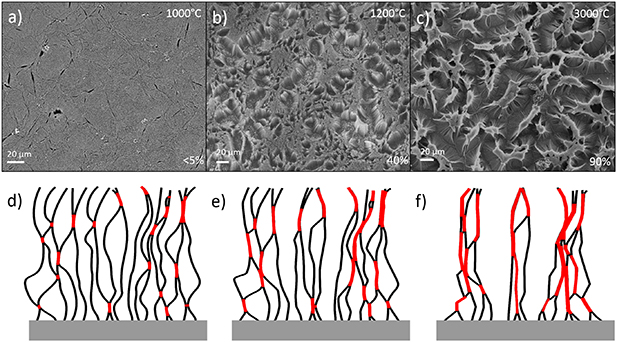
Figure 6. (a)–(c) SEM images of annealed CNT arrays after annealing at 1000 °C, 1200 °C and 3000 °C respectively. Lower right corner shows the degree of densification as measured by the ratio between top surface area to total area. (d)–(f) Illustration of the mechanism of macro-scale densification based on individual CNT bonding. (d) Pristine CNT array with initial inter-CNT contact in red. (e) Partially bonded CNT array with longer bonded regions. (f) Heavily densified CNT array with significant amount of bonded regions of two or more CNTs.
Download figure:
Standard image High-resolution imageFigure 6(d)–(f) illustrate how the bonding of individual CNTs causes this macroscale densification. Adjacent CNTs that are originally in close contact at some points, shown in red, will during heat treatment bond at those points. As the bonded regions grow, those CNTs are attracted to each other as a consequence. In the array, each CNT will have multiple adjacent tubes to connect and bond to, leading to a general attraction between CNTs. The array splits along line of naturally lesser CNT interaction, and forms smaller bundles, leading to the structure in figure 6(c).
The remaining question is why the CNT inter-tube bonding happens in the first place, or rather, since the vdW bonding is very stable once formed, why this bonding does not happen before annealing. A possible explanation is that the defects and functional groups on the outside of the CNTs prevent close contact of large areas of actual CNT surface.
As seen in figure 6(a) and (b) the densification starts between 1000 °C and 1200 °C. Elumeeva et al [31] found that structural improvements of MWCNTs during high temperature annealing starts from the outer layer inwards. It is possible that the heat treatment affects the outer layers of the CNTs enough for binding at 1200 °C even if large structural improvements generally require higher temperatures. However, a more likely cause for the inter-tube bonding is due to the removal of oxygen containing functional groups on the CNTs, which similarly to defect sites could prevent close enough proximity for the vdW forces to dominate. While most functional groups on carbon decompose at lower temperatures [32, 33], the most stable groups such as carbonyl or quinone have a decomposition temperature between 1000 °C and 1200 °C, which fits very well with the onset of densification in this work.
3.5. Elimination of catalyst
In addition to the effect of heat treatment on the CNT array itself, the interface between graphite and CNTs undergoes drastic changes. In particular, pristine CNT arrays still have the Al2O3/Fe catalyst layers between the CNTs and the graphite, which are expected to evaporate at these temperatures [49]. To investigate this evaporation, x-ray photoelectron spectroscopy (XPS) was used to determine the elemental composition of the samples before and after annealing. Due to the densification effect the annealed samples had exposed CNT roots at the bottom of the CNT valleys, which allows signal contributions from the catalyst using a direct measurement from the top of the array. In order to get a comparable measurement for the pristine CNT array, it was densified by capillary forces from submersion in water [50]. After submersion, the water evaporates causing capillary forces and surface tension to pull the CNTs toward each other, which forms a comparable structure and degree of densification as the heat treated samples.
Figure 7 shows the entire XPS spectra for pristine (red) and annealed (blue) graphite/CNT array structures, together with more detailed scans of the peaks corresponding to Fe2p, O1s and Al2p. The elemental composition of the CNT graphite structure based on the data from figure 7 is shown in table 1.
Figure 7. XPS measurement results. Full spectrum of pristine (red) and annealed (blue) CNT/graphite structures. The spectra are normalized with respect to C1s peak intensity (285 eV) and offset for clarity. Insets show further comparisons of the Fe2p peak around 712 eV, O1s peak at 531 eV and Al2p peak at 76 eV.
Download figure:
Standard image High-resolution image
Table 1. Elemental composition of CNT graphite structure determined by XPS.
| (wt%) | C | O | Fe | Al |
|---|---|---|---|---|
| Pristine | 91.19 | 5.23 | 0.12 | 3.46 |
| Annealed | 99.66 | 0.27 | 0.00 | 0.07 |
Before annealing, except from the main carbon 1 s peak at 285 eV, the sample shows additional peaks at 975 eV, 531 eV, 121 eV and 76 eV, corresponding to O KLL, O1s, Al2s and Al2p respectively [51]. These peaks clearly indicate the presence of oxygen and aluminum. I addition, there is a small Fe2p peak at 712 eV, visible in the inset of figure 7, corresponding to a Fe2O3 phase. After annealing, the XPS spectrum is nearly identical to a pure graphite spectrum. There are no visible signal from either aluminum nor iron, as seen in the insets of figure 7, and only a minuscule trace peak of oxygen.
As far as can be detected, the annealing process has completely eliminated the remains of the CVD catalyst structure. A small O1s peak can still be detected in the annealed sample, but the oxygen content has decreased from 5.23% to 0.27%, which indicates that oxygen has largely been eliminated both in the alumina of the catalyst layer, and from oxidized groups on the CNTs themselves. This is consistent with thermal decomposition of functional groups coupled with a greatly reduced number of defect sites which could react with atmospheric oxygen after annealing. This further supports the hypothesis that the onset of densification is due to the removal of functional groups preventing close CNT contact.
The elimination of catalyst does not prove seamless bonding between graphite and CNTs. However, given that odako CVD of CNTs forms covalent bonds between CNT and the topmost graphene layer [11, 16] at much lower temperatures, it is highly likely that it is the case. Further evidence of a stronger connection is evident from a simple mechanical test. Scratching as-grown CNT with a tweezer easily dislodges CNTs from the substrate. After heat treatment, the same scratching rather causes the topmost graphite layers to peel off together with the CNT array, meaning that the bonding between CNTs and substrate is at least stronger than graphite interlayer bonding.
4. Discussion
This study confirms previous studies, which find that heat treatment improves the quality of CNTs and reduces the amount of defects. The larger crystallite size directly corresponds to an increased Young's modulus as previously shown [25]. Using the same model, the Young's modulus of the CNTs in the present study was found to increase by 124%, from 78 ± 52 GPa to 175 ± 102 GPa. This increase is consistent with previous results [31]. Similar improvement is to be expected in terms of thermal and electrical properties as well.
While the effect of heat treatment of CNTs has been investigated previously, the effect of this treatment on an array level has been impractical with common CVD substrate materials such as silicon or quartz. Using graphite as a substrate instead allowed us to anneal the entire array, which has demonstrated the elimination of the CVD catalyst structure and resulting anchoring of the CNT array to the substrate. This type of annealing could be an important step in the creation of future seamless graphite- or graphene-CNT hybrid materials.
The heat treatment of an entire CNT array also highlighted the inter-tube bonding and subsequent array level densification effect. While this bonding and densification effect has, to the authors knowledge, not specifically been investigated previously, it is consistent with previous reports on CNT annealing. For instance, Yang et al [52] reported a decrease in intertube distance after spark plasma sintering at 1500 °C of freestanding aligned MWCNT samples, which is likely due to the same effect. However, the mechanism for this effect has not previously been explained. Due to the substrate keeping one end of the CNTs stationary in our case, the densification is more obvious, and can be quantified to some extent. The onset of densification between 1000 °C and 1200° fits well with experimental measurements of the decomposition of carbonyl functional groups [32], and is a likely mechanism that prevents CNT inter-tube bonding at lower temperatures. However, further research is needed in order to verify this directly.
This effect has important implications for the use of heat treated CNT arrays. At a first glance, the the densification effect appears to limit the usefulness of the resulting hybrid material. The increased roughness makes the material unsuitable for otherwise potential applications, such as thermal interface materials [8, 12]. Furthermore, the densification and inter-tube bonding severely limits the amount of useful surface area, further limiting otherwise promising applications such as supercapacitor electrode [10] or for convective heat dissipation [11]. Further research is necessary in order to understand the drivers and parameters of the densification process, and whether it is possible to tune the process into improving CNT quality without sacrificing array structure.
However, in certain applications, the densification could be a benefit rather than drawback. Denser CNT arrays allow for higher effective electrical and thermal conductivity. Heat treatment of free-standing CNT arrays, such as the one by Wang et al [53] would potentially allow for the entire CNT array to contract as a bulk, potentially increasing the effective array thermal conductivity by as much as an order of magnitude even before considering CNT quality improvements.
Even when still attached on a substrate, smaller bundles of CNTs can still densify as one unit, allowing for a controllable process to create densified CNT pillars [54]. These can subsequently be transferred and used, for instance as through-silicon vias [55, 56] or field emitters [57]. By utilizing heat treatment instead of capillary force based methods, the CNT array density as well as the individual CNT quality could be simultaneously improved.
5. Conclusion
In this work, we have investigated the effect of annealing at 3000 °C on CVD grown CNT arrays on graphite film. We found a dramatic increase in crystallinity and reduced defects, as shown by Raman spectroscopy and TEM imaging. Analysis of the Raman G-band and TEM diffraction reveals a 50% increase in crystallite size and a corresponding 124% increase in Young's modulus. The TEM images show a strong regeneration of graphitic ordering of the CNT structure. At the same time, increased intertube interactions caused adjacent CNTs to align and bond, which on a larger scale causes a densification of the entire CNT array.
Elemental composition analysis using XPS shows that all non-carbon impurities are removed during annealing, including oxygen-containing functional groups as well as the Fe and Al2O3 catalyst structure. This would allow for seamless bonding between the substrate and CNT array.
This study shows the effects of heat treatment of CNTs in a vertically aligned array, which could allow for the use of higher quality CNTs in VACNT applications. At the same time we demonstrate the possibilities and limitations of a new route towards fabrication of seamless graphene/graphite CNT hybrids.
Acknowledgments
The authors would like to thank Shujin Chen at SMIT Center, Shanghai University, China, for the heat treatment processing as well as Per Hyldgaard at the Electronics Materials and Systems Laboratory, Chalmers University of Technology for advice regarding the vdW-DF-cx method and its interpretation. The authors acknowledge the financial support from the Swedish Board for Strategic Research (SSF) with the contract No: SE13-0061 and GMT14-0045, from the Swedish Board for Innovation (Vinnova) under the SIO Grafen program, from Formas with the contract No: FR-2017/0009 and from the Swedish National Science Foundation with the contract No: 621-2007-4660 as well as from the Production Area of Advance at Chalmers University of Technology, Sweden. Finally, we acknowledge the financial support from the EU Horizon 2020 project: Nanosmart. This work was performed in part at Myfab Chalmers.