

Abstract
We report the electrical transport of thin vertically-stacked Josephson tunnel junctions. The devices were fabricated using 16 nm thick GdBa2Cu3O7−δ electrodes and 1–4 nm SrTiO3 as an insulating barrier. The results show Josephson coupling for junctions with SrTiO3 barriers of 1 and 2 nm. Subtracting the residual current in the Fraunhofer patterns, energies of 3.1 mV and 5.7 mV at 12 K are obtained for STO barriers of 1 nm and 2 nm, respectively. The residual current may be related to the contribution of pinholes and thickness fluctuations in the STO barrier. These values are promising for reducing the influence of thermal noise and increasing the frequency operation rate in superconducting devices using high-temperature superconductors.
Export citation and abstract BibTeX RIS
1. Introduction
The development of tunnel Josephson junctions (JJ) is of technological relevance for many applications going from superconducting quantum interference devices (SQUIDS), to radiation detectors and rapid single flux quantum digital electronic circuits [1–5]. Most of them require close-packed arrays of junctions, whose characteristic critical current Ic and normal state resistance Rn have to be uniform over large areas and on large scales from a few to tens of thousands of junctions. The use of high-Tc superconductors (HTS) in JJ, due to the large superconducting gap and operating temperature range [6], offers numerous advantages over other superconducting materials such as Nb [7], nitrides [8] and MgB2 [9, 10]. The large superconducting gap corresponds to a higher Josephson energy, increasing the devices frequency operation rates, relaxing the cooling requirements and reducing significantly the influence of the thermal noise (IN) [11]. Most research in JJ based on HTS such as YBa2Cu3O7−δ is oriented to planar arrays developed using ion irradiation [12, 13], edge ramp [14, 15] and bicrystals [16–20]. The design and fabrication of vertically-stacked JJ allows an increased functionality by using barriers with different electronic and magnetic properties. Nevertheless, few reports have been published to this date [21]. The main obstacle for its design is related to the 3D growth mechanism usually observed in HTS thin films. If the electrodes display huge roughness, then thick barriers of several nanometers are required to reduce the influence of pinholes and to have Josephson coupling. Moreover, the performance of JJ is affected by suppression of the properties at the interfaces [22, 23].
In this letter, we report the electrical properties of superconductor/insulator/superconductor (SIS) vertically-stacked tunnel junctions using thin GdBa2Cu3O7 (GBCO) as superconducting electrodes and SrTiO3 (STO) as the insulating barrier. GBCO is a superconducting material with critical temperature Tc ∼ 93 K. STO is a dielectric material [24] and ferroelectricity (FE) may be induced by strain [25]. GBCO has an orthorhombic structure with lattice parameters of a = 0.383 nm, b = 0.389 and c = 1.17 nm. STO is a cubic perovskite with a = 0.3905 nm. The crystalline structure of GBCO/STO/GBCO trilayers was previously discussed in [26]. In our research, the GBCO thickness of 16 nm was selected by considering a trade-off between Tc and the presence of smooth surfaces [22, 26]. The low surface roughness of the electrodes is critical to be able to fabricate JJ with ultra-thin insulating barriers (i.e. with only a few nanometers). The heterostructures display single phase with (00l) orientation. The STO surface displays steps which are mainly originated by the roughness of the bottom GBCO electrode (typical 1 unit cell ∼1.2 nm) [22]. The barrier thickness displays typical fluctuations of around 1 STO unit cell [26]. In addition to the thickness fluctuations, the properties of the junctions may be affected by the stacking order at the interfaces, oxygen vacancies and by crystalline defects [27, 28]. The electronic homogeneity of the STO barrier as a function of the thickness was previously analyzed in GBCO/STO bilayers by conducting atomic force microscopy at room temperature [29]. Conductivity maps indicate higher values at the borders of 3D defects than in the terraces and a barrier thickness distribution width of 0.8 nm. The Tc of 16 nm thick GBCO films is Tc ∼77 K. Moreover, for GBCO/insulator bilayers the Tc value decreases from ∼77 to ∼ 40 K when the barrier thickness increases from 1 to 4 nm [30]. The reduction in Tc could be related mainly with the stress induced by the substrate and the barrier, probably modifying the oxygen content [31].
2. Experimental
The epitaxial GBCO/STO/GBCO trilayers were grown by sputtering on STO substrates using the conditions previously described in [22, 26]. The dsubstrate temperature was kept at 730 °C in an Ar (90%)/O2(10%) mixture at a pressure of 400 mTorr. After deposition, the temperature was decreased to 500 °C, and the O2 pressure was increased to 100 Torr. Finally, the samples were cooled down to room temperature at a rate of 1.5 °C min−1. A 2 nm thick STO buffer layer was introduced to reduce the nucleation of 3D defects in the GBCO bottom electrode [22]. The tunnel junctions design used 16 nm thick GBCO electrodes and a STO barrier with thickness (dSTO) of 1, 2, 3, and 4 nm. Wherever used, the notations [G-dSTO-G] indicate a GBCO bottom and top electrodes and a STO barrier with thickness d (nm). The results presented in this work correspond to JJ using GBCO electrodes with very thin STO barriers and an area of 400 μm2. Figure 1 shows a schematic picture of a tunnel junction. Initially the samples are covered with 10 nm thick Ag using sputtering (to protect the surface). The fabrication process includes successive steps of optical lithography and Argon ion milling [32]. The first step includes optical lithography using a positive photoresist to create square pillars (20 μm × 20 μm), followed by ion milling to remove the top GBCO electrode. The second step involves optical lithography using positive photoresist to create square pillars of 10 μm × 210 μm on the center of the pillars generated at the first step. Third, the junction is covered with a 100 nm thick SiO2 layer by RF sputtering. Finally, the area of 10 μm × 10 μm on the top of the junction is open by lift-off process removing the remaining photoresist using acetone. A path of silver is deposited on the silicon layer to facilitate the electrical connections. Characteristic current–voltage (IV) measurements were obtained using the standard four-point geometry in a closed cycle refrigerator with a base temperature of 12 K. The current was applied using a Keithley source. Each point in the curves is the average of 50 measurements. After the change of the current, a 30 s delay time is used before starting with the voltage measurements. A magnetic field H parallel to the barrier surface was applied with a copper coil. It is important to note that the ion-milling process described earlier suppresses the Tc at the electrical paths provided by the bottom electrode. For this reason, superconductivity at the bottom electrode is expected only in the area under the junction. The Tc value in trilayers is usually higher than 80 K, being dominated by the transition temperature of the top electrode [30]. In this work, we will define Tc from the Josephson coupling temperature (TJ).
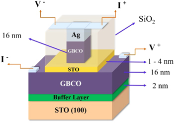
Figure 1. Representative scheme of the materials used in the standard four-point geometry.
Download figure:
Standard image High-resolution image3. Results and discussion
Figure 2 shows typical IV curves of JJ with very thin insulator barriers for temperatures ranging from 12 to 100 K. The slope of the IV curves (emphasized by the dotted line) corresponds to the normal-state junction resistance Rn. Josephson coupling is observed for STO barriers with thicknesses of 1 and 2 nm. The IV curves for [G-3-G] show features related to superconductivity below 35 K, however as we will discuss below, the effect does not correspond to a Josephson coupling. The criteria for Ic determination is indicated in figure 2(b) and corresponds to the departure from the superconducting state (usually abrupt). A low ohmic resistance is observed for [G-2-G], the effect may be related to the silver top layer used to improve the electrical contact at the top electrode (see figure 1). According with these results, the Josephson coupling appears at thickness similar than the coherence length ξ, which is expected to be between 1 and 2 nm for the GBCO electrodes (as Tc reduces, the ξ increases) [33]. Considering inhomogeneous barriers, the Josephson coupling should be affected by fluctuations in its thickness [34]. Moreover, the effective barrier thickness may be affected by oxygen vacancy migration [28]. The absence of coupling for [G-3-G] and [G-4-G] may be related mainly with an effective thickness larger than ξ. The IV curves in [G-4-G] show features usually observed in metal-insulator-metal junctions [26]. The Rn values are 1.6 Ω [G-1-G], 99 Ω [G-2-G] and 550 Ω [G-3-G], indicating a significant increment in the resistance of the junctions when the STO thickness is increased. As expected, increasing the barrier thickness reduces TJ ranging from ∼77 K for [G-1-G] to ∼35 K for [G-3-G]. This effect could be potentiated in these junctions due to the decrease of the Tc with increasing barrier thickness [30]. It is important to note that the IV measurements for [G-1-G] show hysteresis, which is usually associated with an underdamped behavior (characteristic of SIS junctions), while the IV curves for [G-2-G] do not show hysteresis, corresponding to the overdamped behavior. For the latter, due to a higher Josephson energy, a reduced influence of thermal fluctuations leads to smaller variations in the switching behavior.
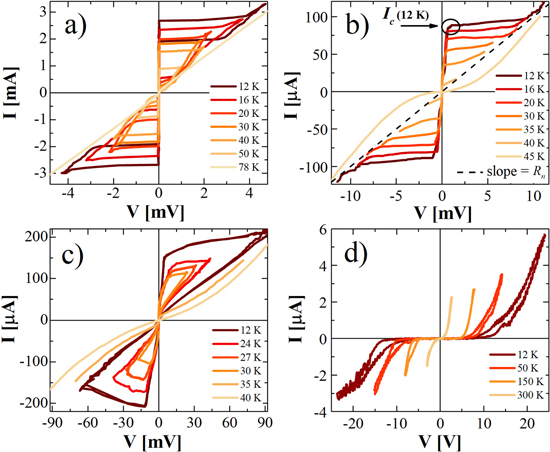
Figure 2. Characteristic IV curves at different temperatures for (a) [G-1-G]; (b) [G-2-G]; (c) [G-3-G]; and (d) [G-4-G]. The curves are obtained applying current and measuring voltage. Josephson coupling is observed for JJ with STO barriers of 1 and 2 nm. The criteria for the determination of Ic and Rn are indicated in (b).
Download figure:
Standard image High-resolution imageIn order to verify the presence of Josephson coupling, we investigated the effect of the external magnetic field H perpendicular to the Josephson current. For that, we performed IV measurements applying different magnetic fields (see figures 3(a) and (b)). The Fraunhofer patterns display the expected periodic modulation with minima spacing ΔH ∼ 30 G. A distinctive feature of the patterns is a residual current at the minima. This may be interpreted as the presence of short circuits (pinholes) or to an inhomogeneous current density distribution in the junction [35]. Considering thickness fluctuations and effects produced by different interfaces stacking, it is expected that both effects contribute. As we have shown previously for GBCO/STO bilayers, the electrical conductivity at the border of 3D defects is significantly higher than the one in the terraces [29, 30]. If the borders of the 3D defects are pinholes (short circuits), Ic is originated by two contributions: Josephson IJ (terraces) and pinholes Ip (borders of 3D defects). The Ip values for [G-1-G] and [G-2-G] at 12 K (minima 1) are ∼290 μA and ∼30 μA, respectively. According to this scenario, IJ decreases faster than Ip when the STO thickness is increased. This is consistent with our measurements indicating that Ic ∼ Ip for [G-3-G] (see below).

Figure 3. Ic modulation by an external magnetic field for: (a) [G-1-G]; (b) [G-2-G]. The straight and dotted lines correspond to the fit for an ideal JJ using equations (1) and (2), respectively. Inset (a) shows a schematic tunnel junction and the magnetic field configuration. The right part of the panel (a) shows a schematic representation of the effect of the magnetic field on the tunneling currents in a uniform junction. Inset (b) shows typical I–V curves obtained at 16 K for different applied magnetic fields. The curves are obtained fixing the magnetic field, applying a current and measuring the voltage.
Download figure:
Standard image High-resolution imageThe expected field dependence of the Ic for rectangular JJs is given by:
here I0 = J1WL (J1 the total current density, W and L the lengths of the junction), H0 is the value of the magnetic field corresponding to a flux quantum penetrating into the junction. For inhomogeneous barriers with non-zero residual currents where the thickness fluctuations are small in comparison with the thickness of the barrier, the Fraunhofer pattern may be described by [36]
where  is the mean-square of the current fluctuations across the barrier and N is a factor that represent the thickness fluctuation (N > 1 for small fluctuations). The fits for a homogenous (equation (1)) and inhomogeneous (equation (2)) barriers are included in figures 3(a) and (b). The former reproduces the modulations but no the residual current. For the application of equation (2) it is necessary to consider a factor
  The values of Ic at the minima differ from zero and are γIo. The data for [G-1-G] and [G-2-G] qualitatively reproduce with γ = 0.083 and 0.28, respectively. The model considers that residual current at the minima is constant in field. According with the model a large γ corresponds to small N and large thickness fluctuations. The magnetic field dependence of the residual current experimentally observed may be related to large thickness fluctuations and also to a pinhole background.
It is important to mention that the IV measurements for [G-3-G] display a different behavior than [G-1-G] and [G-2-G] (see figure 4). No Josephson coupling was observed for this sample, suggesting that the measured superconducting current originates in the electrodes and propagates through pinholes. When the voltage polarization is up, the curves show a step-like transition to a normal state (current is injected from the top to the bottom electrode), however, when the voltage polarization is inverted the normal state remains until a characteristic voltage where a reentrant superconducting state is observed. Suppression of the superconducting state with voltage polarization has been previously observed in superconducting/FE bilayers [37]. It is known that ferroelectricity appears in strained STO [25]. In this scenario, the jumps for the increment / decrement of the resistance could be originated by the switching of the FE domains [38]. The asymmetric properties for the voltage polarization could be related to different Tc for the bottom and top electrodes. Although in [G-3-G] the IV curve is dominated by pinholes (Ip∼Ic), the results show that the polarization suppresses the superconducting currents. No features related to changes in the IV measurements induced by polarization are observed in [G-4-G].

Figure 4. Current versus voltage measurements for [G-3-G] at different temperatures. The arrows indicate the path in which the current is applied. P indicates the direction of the polarization (up: from bottom electrode to top electrode; down: from top electrode to bottom electrode). The curves are obtained applying current and measuring voltage. Hysteretic behavior is observed for temperatures below 30 K.
Download figure:
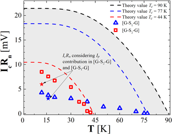
Standard image High-resolution imageFigure 5 shows the temperature dependence of IcRn for [G-1-G] and [G-2-G]. For SIS with identical superconductors, the theoretical temperature dependence of IcRn is limited by the gap as

where ![${\rm{\Delta }}\left(T\right)=\,{\rm{\Delta }}\left(0\right)\tanh \left\{1.82{\left[1.018\left(\tfrac{{T}_{c}}{T}-1\right)\right]}^{0.51}\right\}$](https://content.cld.iop.org/journals/0957-4484/31/10/105701/revision2/nanoab59f7ieqn3.gif) [39] and
[39] and  It is important to note that for d-wave superconductors the Ic (T) curves could display a non-monotonic behavior due to changes in the superconducting lobes that contribute to the tunneling [40] (not considered in our analysis). The results show that at 12 K (our lower temperature), the IcRn value is strongly affected by the barrier thickness and by the reduction in the Tc of the electrodes. The [G-1-G] displays IcRn (12 K) = 4.2 mV and systematically decreases to disappear close to 77 K. [G-2-G] displays IcRn (12 K) = 8.9 mV and systematically decreases to disappear at approximately 44 K. The values at 16 K and 12 K subtracting the residual current at the first minima are ∼3.1 mV and ∼5.7 mV for [G-1-G] and [G-2-G], respectively. A possible explanation for the reduction in its value for [G-1-G] could be related with the barrier uniformity covering the base electrode. A non-uniform covering of the electrode may result in junction areas with thick barrier that does not contribute to the total IJ but provides a resistive shunt to the junction. Moreover, regions with very thin barriers may result in superconductor/normal/superconductor (S/N/S) coupling due to oxygen vacancies [28]. Similar behavior (IcRn lower than the theoretical value) has been observed in MgB2/TiB2/MgB2 junctions [10]. In our case, the performance of the junction is significantly improved for 2 nm STO barriers where a higher covering of the electrode is expected.
Figure 5. Comparison of IcRn measured in [G-1-G] and [G-2-G] with the theoretical expectations according to the equation (2). The dashed lines correspond to the expected values considering Tc of 44, 77 and 90 K.
Download figure:
Standard image High-resolution image
The value of IcRn (12 K) ∼5.7 mV (subtracting residual current) is larger than that generally observed in NbN [8] and MgB2 [41] tunnel junctions. For instance, for NbN the theoretical maximum IcRn given by the gap is ∼4 mV and for MgB2 junctions the reported values at 4.2 K are ∼2 mV [42, 43]. Moreover, the IcRnvalues obtained for JJ with ultra-thin barriers are larger than the ones usually observed in ion irradiated YBCO JJ [44, 45]. The large Josephson energy in [G-1-G] and [G-2-G] at low temperatures is evidenced from the IV curves with low IN [11]. Nowadays, with the existence of high-performance cryogenerators, the TJ value is not an issue. Moreover, the quantum effects tend to wash out as a consequence of thermal noise when the operation temperature is increased, which becomes critical for superconducting devices operation. A high Josephson energy is essential for the development of high-quality JJ for two factors, reduced influence of thermal noise and a higher operating frequency.
4. Conclusions
In summary, we have fabricated vertically stacked GBCO/STO/GBCO tunnel junctions with ultra-thin STO barriers. Josephson coupling is observed for GBCO/STO/GBCO tunnel junctions with STO barriers of 1 nm and 2 nm. The IcRn values are affected by the presence of pinholes and fluctuations in the barrier thickness. For thin insulator barriers, the presence of short circuits tends to reduce the IcRn value. Moreover, S/N/S coupling cannot be discarded. Subtracting the residual current in the Fraunhofer patterns, we obtain IcRn (12 K) = 5.7 mV, which is close to the theoretical prediction for JJ with Tc ∼ 27 K. The use of thin GBCO electrodes with low surface roughness allowed the fabrication of JJs using very thin insulating barriers. These junctions present high IcRn values reducing the thermal noise and increasing the response and frequency operation of the JJs. These are promising results for the development of superconducting devices.
Acknowledgments
This work was partially supported by the ANPCYT (PICT 2015-2171). HN, MS and NH are members of the Instituto de Nanociencia y Nanotecnología CNEA-CONICET (Argentina).