

Abstract
Metal-phosphorus-trichalcogenides (MPTs), represented by NiPS3, FePS3, etc, are newly developed 2D wide-bandgap semiconductors and have been proposed as excellent candidates for ultraviolet (UV) optoelectronics. In spite of having superior advantages for solar-blind UV photodetectors, including those free of surface trap states, being highly compatible with versatile integrations as well as having an appropriate band gap, to date relevant study is rare. In this work, the photoresponse characteristic of UV detectors based on few-layer FePS3 has been comprehensively investigated. The responsivity of the photodetector, which is observed to be determined by bias gate voltage, may achieve as high as 171.6 mAW−1 under the illumination of 254 nm weak light, which is comparable to most commercial UV detectors. Notably, both negative and positive photoconductivities exist in the FePS3 photodetectors and can be controllably switched with bias voltage. The eminent and novel photoresponse property paves the way for the further development and practical use of 2D MPTs in high-performance UV photodetections.
Export citation and abstract BibTeX RIS
1. Introduction
Ultraviolet (UV) photodetectors are usually very sensitive in light detection with short wavelength (typically less than 400 nm), owning to their advantages of high wave-selectivity and low natural-light radiation [1]. These features promiss broad applications ranging from the military domain, including missile early warning, and secure optical communication to civilian use as environmental monitoring, biological and chemical analysis, etc [2–4]. In general, wide-bandgap semiconductors such as GaN [5], ZnO [6], SiC [7], diamond and most recently Ga2O3 [8] are appropriate candidates for UV-absorbing materials. However, the performance of wide-bandgap semiconductor-based photodetectors currently encounters challenges of slow response and recovery speed caused by surface trap states [9]. In addition, the requirement of the unavoidable epitaxy process hinders the compact integration and further development of devices based on these materials.
Compared with a conventional semiconductor, 2D materials exhibit distinct advantages in solving the above problems for photodetection applications. They are free of dangling bonds on the surface, which reduces the scattering centers and hence promises a shortened response time by accelerating the photogenerated electron–hole pairs [10]. Furthermore, the atomic thick feature together with the possibility of van der Waals integration allows for high compatibility with versatile systems and microfabrication techniques [11, 12]. Graphene and transition metal dichalcogenides (TMDCs) have been proposed and well developed for photodetectors [13–15]. The relatively small band gap (Eg < 2 eV) of these materials limits their optoelectronic applications in the UV regime. Although a broadband response (including UV band) could be realized with modified graphene [16], with TMDCs [17] and their heterostructures [18–20], the wave selection is still a barrier in general. Developing 2D materials with a suitable band gap for UV photodetectors is crucial. Wide-bandgap 2D semiconductors, have thus attracted considerable interest in realizing reliable performance for UV detection with high detectivity and fast response, while retaining the merits of 2D materials. Metal-phosphorus-trichalcogenides (MPTs), represented by NiPS3, FePS3, etc, are newly developed 2D semiconductor materials with similar atom structure to TMDCs, while having an intrinsic large band gap (up to 3.5 eV) [21]. Because of the suitable band gap and theoretically predicted high carrier mobility, MPTs are suggested as excellent candidates for UV detectors, but reports of these materials are rare. Most recently, He et al for the first time attempted a UV photodetector based on few-layer NiPS3 nanosheets, which shows remarkable photoresponse together with fast response speed [22]. There is still room for improving the metrics of the MPT-based UV photodetectors.
In this work, we comprehensively investigated the photoresponse of another novel MPT member, FePS3, which possesses a 2 eV band gap and a higher conductivity compared to NiPS3 [23, 24]. It was found that, despite the obvious sensitivity to deep UV light illumination (wavelength of 254 nm), the responsivity of the detector with few-layer FePS3 was determined by bias voltage. More interestingly, both negative photoconductivity (NEC) and positive photoconductivity (PEC) exist and can be switched under bias control for the fabricated FePS3 photodetectors. The correlated mechanism was also well clarified in illuminating the optimizing route for the practical use of 2D MPTs in high-performance UV photodetections.
2. Experimental details
2.1. Synthesis of FePS3
A stoichiometric amount of high-purity elements (Fe: 99.99%, 1.221 g; P: 99.999%, 0.677 g; S: 99.99%, 2.102 g) and 0.1 g of iodine as the transport agent were sealed into a quartz ampoule (15 cm in length and 1.5 cm in diameter) under vacuum, which was then set in a horizontal furnace over a temperature gradient from 700 °C–630 °C. After being heated for 2 weeks, the ampoule was cooled down to room temperature and black plate-like crystals with metallic luster were formed in the deposition zone.
2.2. Material characterizations
X-ray powder diffraction (XRD) patterns were recorded on a Rigaku SmartLab Intelligent XRD system with filtered Cu Kα radiation (λ = 1.5406 Å, operating at 45 kV and 200 mA). Transmission electron microscopy (TEM) images, high-resolution transmission electron microscopy (HRTEM) images, selected area electron diffraction (SAED) patterns, an energy dispersive x-ray spectroscopy (EDS) elemental mapping were taken from a JEM-2100F (field emission) scanning transmission electron microscope (JEOL, Japan) with an acceleration voltage of 200 kV. Raman measurements were performed in a Horiba HR Evolution, where the excitation was provided by light (λ = 532 nm) through a 100×objective. Thickness was measured with an atomic force microscope (AFM, Bruker Icon). A spectrophotometer (Lambda 750) was employed to acquire UV–vis absorbtion spectra.
2.3. Device fabrication and measurements
To fabricate field-effect transistors (FETs), few-layered FePS3 nanosheets were first obtained through a mechanical exfoliating method using a blue Nitto tape. Then the obtained sheets were transferred onto a Si/SiO2 (285 nm) substrate by the commonly used dry transfer method. An optical microscope was used to select the samples with a thickness of 10–20 nm. An AFM (Vecco Dimension3000) was used to confirm the thickness. Electron beam lithography (JEOL JBX 5500) was used to define source and drain electrode patterns, and Cr/Au (10/90 nm) film was deposited onto the substrates using an electron beam evaporator (ULVAC Ei-5Z). The photodetectors have the same structure as the FETs mentioned above. All the measurements were performed in a vacuum probing station at room temperature with a vacuum of 10−4 Pa. The data were collected with a Keithley 4200 semiconductor parameter analyzer. A light source with 254 nm wavelength was used to illuminate the devices. The power density was measured to be 0.18 mW cm−2.
3. Results and discussion
The crystal structure of the synthesized FePS3 is shown in figure 1(a). Generally, FePS3 has CdCl2 type-structure [25] in which S atoms occupy the Cl sites forming layer lattices with double layers, and one third of the Fe atoms are substituted by P-P pairs. Fe atoms and P-P pairs are filled in the octahedral centers of the S-sublattice forming P2S6 bipyramid units. Each S atom bonded to a single P atom and two Fe atoms. In this case, Fe atoms and P-P pairs are sandwiched between the sulfur double layers resulting in lamellar structures. Therefore, it is often expressed as hexachalkogenohypodiphosphate, i.e. 3 [SFe2/3(P2)1/3 s] = Fe2P2S6. These layers are weakly bonded through van der Waals S-S interactions, and hence, a 2D nanostructure can be easily prepared by a clear method such as exfoliation. As shown in figure 1(b), a large amount of FePS3 flakes with an average size of ∼3 mm can be obtained during synthesis. Figure 1(c) shows the AFM image of the exfoliated few-layer FePS3 nanosheet, the thickness of which is about 15 nm. Figure 1(d) shows the typical XRD patterns of the prepared sample. All the diffraction peaks can be readily indexed to the monoclinic structure of FePS3 with the calculated lattice constants of a = 5.9484 Å, b = 10.2997 Å, c = 6.7215 Å and β = 107.16°, which are perfectly consistent with the reported data (JCPDS Card File No. 78−0496, a = 5.947 Å, b = 10.300 Å, c = 6.722 Å and β = 107.16°). No characteristic reflection peaks originated from other components such as iron sulfides, iron phosphides or corresponding elements, indicating the pure phase of FePS3. Raman spectra were collected using a 532 laser in ambient conditions. As shown in figures 1(e), 99.8, 157.2, 226.4, 247.5, 279.1 and 380.1 cm−1 can be identified in both bulk and layered FePS3, which is consistent with a previous report [21]. The peaks ranging from 85–100 cm−1 originate from the Fe atom vibration in FePS3 [26]. The peak P1 (99.8 cm−1) in FePS3 bulk that shows a broad line shape, could be decomposed into two or more peaks. The intensity of these decomposed peaks may be affected by the thickness of the sample [27]. In few-layered FePS3, the intensity of some decomposed peaks becomes stronger and an extruded peak around 90.4 cm−1 would appear.
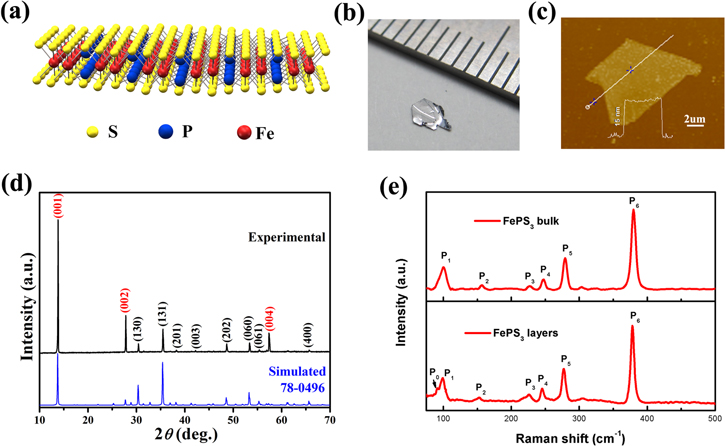
Figure 1. (a) Atomic structure of FePS3. (b) Typical optical image of synthesized FePS3 flakes. (c) AFM image of an exfoliated few-layer FePS3 nanosheet with thickness of 15 nm. (d) XRD pattern of FePS3 and its corresponding lattice planes. (e) Raman spectra of bulk and few-layered FePS3.
Download figure:
Standard image High-resolution imageTo further evaluate the quality of the synthesized FePS3, microstructure and chemical component analysis were carried out by employing TEM, SAED and EDS. Figure 2(a) presents a typical TEM image of the obtained few-layer FePS3 nanosheet sample, demonstrating the clear 2D nanosheet structures. The corresponding SAED patterns recorded along the [001] zone axis can also be perfectly indexed as the monoclinic FePS3 structure and the single-crystalline nature of the nanosheets (inserted in figure 1(a)). To further investigate the microstructure of these FePS3 nanosheets, HRTEM was performed. As displayed in figure 2(b), the HRTEM image exhibits 2D atomic lattice fringes, suggesting a good crystallinity of the nanosheets. The three characterized interplanar spacings are measured to be 0.28, 0.29 and 0.29 nm, which match well with the (200), (130) and  planes of the monoclinic structure of FePS3 phase. As shown in figures 2(c)–(f), the EDS elemental mapping images exhibit a uniform distribution of Fe, P and S elements, further confirming the formation of FePS3 phase.
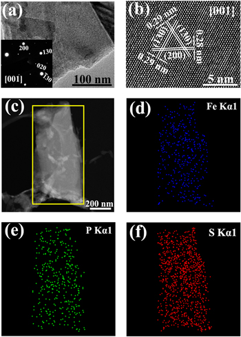
Figure 2. (a) Typical TEM micrograph of FePS3 nanosheet and the inset shows the corresponding SAED pattern. (b) HRTEM image for the FePS3 nanosheet. (c)–(f) EDS element mapping images.
Download figure:
Standard image High-resolution imageThe measurements of the electrical characteristic and photoresponse of the FePS3 share the same FET device structure, with 254 nm wavelength light illumination as the optical source (schematically shown in figure 3(a)). A typical profile of the device is given by the AFM scanned image in figure 3(b), where the thickness of the FePS3 nanosheet is usually chosen to be ∼10 nm. The output curves exhibit linear variations under different gate voltage bias (figure 3(c)), which indicate a good ohmic contact between the FePS3 nanosheet and metal electrodes. UV–vis spectroscopy was used to measure the absorbance of the FePS3 nanosheet (figure 3(d)) and a clear UV photoresponse characteristic can be observed, with much stronger absorption in the regime of wavelength less than 450 nm. Figure 3(e) shows the time dependence of the photocurrent of an 11 nm thick FePS3 photodetector under a fixed Vds of 60 mV and zero gate bias with a weak illumination of 254 nm wavelength light (power density ∼0.18 mW cm−2). It is obvious that the photocurrent shows a rapid decrease upon the illumination, representing NEC. The responsivity is a key factor to characterize the performance of photodetectors, which is defined as R = Iphoto/Pincident, where, Iphoto is the photocurrent and Pincident is the incident power. At zero bias, R is calculated to be 12.3 mA W−1 for the as-prepared few-layer FePS3 photodetector. And, the detector can be effectively switched on/off upon the switching of the illumination. As shown in figure 3(f), the rise and decay time of the device is very short with measured values of 105 and 120 ms, respectively. Both the rise time and decay time are comparable with most of the detectors based on TMDCs [28, 29].
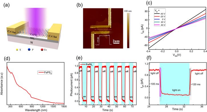
Figure 3. (a) Schematic diagram of a FePS3 UV photodetector. (b) AFM image of a two-terminal FET device based on few-layer FePS3 nanosheet with thickness of ∼11 nm. (c) Output characteristics of the FePS3 FET as a function of gate voltage bias ranging from −40 V to 40 V. (d) UV–vis absorption spectrum of a typical few-layer FePS3 nanosheet. (e) Time-dependent photocurrent of the FePS3 photodetector. Incident light: 254 nm, Vds = 60 mV, and Vg = 0 V. (f) Photoresponse time of the FePS3 detector. Rise and decay time are 105 and 120 ms, respectively.
Download figure:
Standard image High-resolution imageAs gate voltage bias usually has a significant impact on the photodetector's performance, a series of discontinuous gate voltage bias were added to the device accordingly in our experiment to check the dependence. With the application of gate voltage bias, the device displays tunable responsivity, which depends on voltage bias. In addition, the device exhibits different response modes, namely PEC and NEC when turning the bias from negative gate voltage to a positive one. Figure 4(a) shows the general statistics of the responsivities under different gate voltage bias. In the negative bias range, the responsivity increases exponentially with the decrease of bias, and reaches 171.6 mAW−1 when the voltage is −40 V, which has a more than three times enhancement relative to that at −20 bias and is comparable to the traditional UV detectors [30, 31]. In the positive scope, the responsivity shows approximative linearization in contrast to the increase of voltage bias. Figures 4(b)–(d) are specific time-dependent responsivity measurements under different negative bias, while figures 4(e)–(g) show the responsivity details under different positive bias.
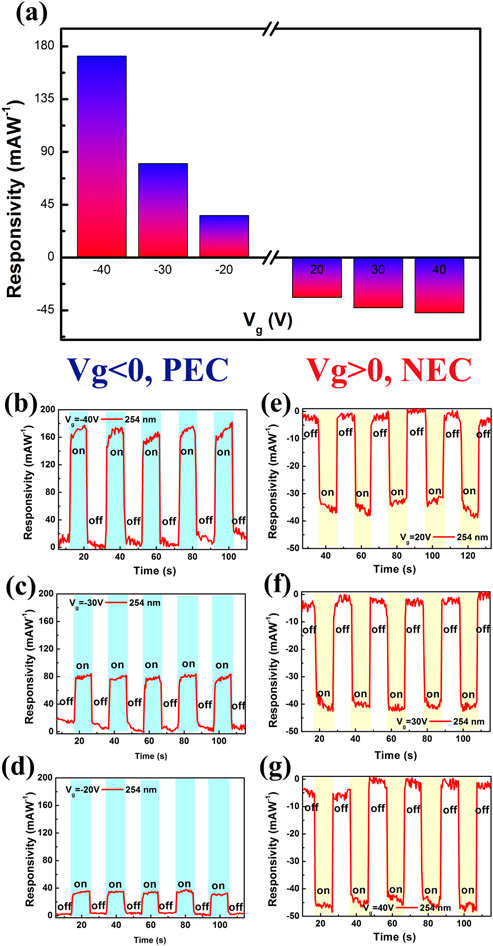
Figure 4. (a) General statistics of responsivity of a FePS3 photodetector at different gate voltage bias. (b)–(d) PEC response under different negative bias. (e)–(g) NEC response under different positive bias.
Download figure:
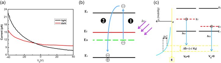
Standard image High-resolution imageIt is novel and interesting that the photodetector displays two modes of photoconductivity response, which are controllable by bias gate voltage. Exploring the internal mechanism is important and meaningful for the further optimization of MPT-based UV photodetectors. Figure 5(a) shows transfer curves of the device with the illumination on and off, for comparison. A fixed Vds of 60 mV was supplied with Vg ranging from −40 V to 40 V, under illumination of 245 nm (power density ∼0.18 mW cm−2). Besides the obvious p-type conduction mode, we can see clearly that the photocurrent changes more dramatically under illumination, which is much higher in the negative part and decreases drastically to the lower standard when a positive bias is provided. The photocurrent is proportional to conductivity σ. For FePS3, the hole concentration p and hole mobility  play important roles in the process as a p-type semiconductor, according to the formula
  (with μ being mobility ration and p being hole concentration). The physical mechanism for the NEC and PEC could be explained by the competition between
  and p. Figure 5(b) shows the decay of p under illumination. A p-type semiconductor is dominated by acceptor levels, but the minority carrier and corresponding energy level induced by defects [32], co-doping [33], hydrogen sorption [34] and interface impurities [35] can also play an important role in devices [36]. As for FePS3, the donor energy level could be brought in by CVT-induced defects, possible O dangling bonds on the SiO2 surface, hydrogen absorption [37] and replacement between the P atom and S atom. When the light is on, some electrons on donor level (Ed) absorb the photon energy and are excited to the conduction band, corresponding to process ❶. Then, process ❷ occurs, the photon-excited electrons will recombine with holes on the valence band, thus reducing the hole concentration. Figure 5(c) shows the variation of
  according to bias. With the light on, holes on Fermi level (Ef) were excited to
  Subtracting the energy difference between
  and
and  the remaining photon energy will be left for the photo-excited hole's kinetic energy. And it is reasonable that the hole's mobility will be higher for higher hole kinetic energy, as shown in figure 5(c) (left). When more negative bias is applied,
  will shift down towards
  leaving more energy and higher mobility for the photo-excited holes [38]. In this sense, the higher the bias was provided, the higher the
  was obtained.
Figure 5. (a) Transfer curve of the FePS3 photodetection device with and without illumination. Light wavelength: 254 nm, Vds = 60 mV. (b) Processes show the decaying of hole concentration. (c) Gate voltage bias adjusts the Fermi level, leading to the difference in hole mobility.
Download figure:
Standard image High-resolution image
4. Conclusion
In summary, a typical 2D wide-bandgap semiconductor, FePS3 flakes with high crystallinity and uniformity were synthesized. The gate bias voltage regulation of few-layer FePS3 UV detectors demonstrates an impressive performance. The response and decay time of the detector is as fast as 105 and 120 ms, respectively. Under weak illumination, the responsivity shows an obvious enhancement with bias voltage and reaches 171.6 mAW−1 at −40V. In addition, the detector manifests a novel photoresponse characteristic, which responds with a switch of PEC to NEC with the change of gate voltage bias. This eminent and novel property may promote the further optimization of the MPT-based UV photodetectors.
Acknowledgments
This work was supported by the National Natural Science Foundation of China (Grant Nos. 11574349, 11474088, 51761145025), the Natural Science Foundation of Jiangsu province (Grant Nos. BK20150365, BK20170424) , the Natural Science Foundation of Hubei Province (Grant No. 2016CFA081), the Key Research Program of Frontier Sciences of Chinese Academy of Sciences (QYZDB-SSW-SLH031), and the Hundred Talent Program of Chinese Academy of Sciences. S L acknowledges the financial support from the National Natural Science Foundation of China (21461014), the Project for Young Scientist Training of Jiangxi Province (20153BCB23022, and the Natural Science Foundation of Jiangxi Province (20151BAB206016).