
Abstract
Hybrid organic photovoltaic (OPV) cells based on conjugated polymer photoactive materials are promising candidates for flexible, high-performance and low-cost energy sources owing to their inexpensive materials, cost-effective processing and ease of fabrication by simple solution processes. However, the modest PV performance obtained to date—in particular the low power conversion efficiency (PCE)—has impeded the large scale deployment of OPV cells. The low PCE in OPV solar cells is mainly attributed to the low carrier mobility, which is closely correlated to the transport diffusion length of the charge carriers within the photoactive layers. The 2D graphene material could be an excellent candidate for assisting charge transport improvement in the active layer of OPV cells, due to its huge carrier mobility, thermal and chemical stability, and its compatibility with the solution process. In this work, we report on the improvement of the optoelectronic properties and photovoltaic performance of graphene nanoplatelet (GNP)-doped P3HT:PCBM photoactive blended layers, integrated into a bulk heterojunction (BHJ) organic-photovoltaic-based device, using PEDOT:PSS on an ITO/glass substrate. First, the light absorption capacity was observed to increase with respect to the GNP content, while the photoluminescence showed clear quenching, indicating electron transfer between the graphene sheets and the polymeric matrix. Then, the incorporation of GNP into the BHJ active layer resulted in enhanced PV performance with respect to the reference cell, and the best PV performance was obtained with 3 wt.% of GNP loading, with an open-circuit voltage of 1.24 V, a short-circuit current density value of 6.18 mA cm−2, a fill factor of 47.12%, and a power conversion efficiency of about 3.61%. We believe that the obtained results contribute to the development of organic photovoltaic devices and to the understanding of the impact of sp2-bonded carbon therein.
Export citation and abstract BibTeX RIS
1. Introduction
Meeting the emerging need for sustainable energy sources could be achieved through the realization of large-scale, cost-effective and easy-to-process solar cells. In this context, the field of research and development revolving around organic photovoltaic devices (OPVs) based on conjugated polymers and/or small molecules is very exciting and is growing rapidly since these organic materials are efficient light absorbers and their optoelectronic characteristics can be tuned via chemical synthesis. However, although OPVs are showing promising potential, they have not yet been fully deployed, and improving the PCE and increasing their lifetime could significantly expedite their uptake. To address these performance gaps, the development of materials with improved exciton dissociation interfaces and charge collection efficiency is critical [1–3].
Since the pioneering work of Tang [4] on PV devices based on the electron-donor (D)/electron-acceptor (A), there have been significant achievements, particularly in the investigation of bulk heterojunction (BHJ) devices using conjugated carbonaceous polymers and C60 fullerene as a photoactive acceptor material [5–11]. In these BHJ devices, the generated photocharges may be dissociated into free carriers at the interfaces between the donor and acceptor nanodomains. These photocharges are then directed to the charge collection electrodes by the constitutive electric field of the device [12–18]. Implementing this approach with polythiophene/fullerene-composite-based PV devices has led to enhanced power conversion efficiency values [19–23], which are still, however, below those attainable by their inorganic semiconductor-based counterparts [24]. In spite of this technological advancement, the PV performance of the polymer/fullerene composites is still limited by the weakly controlled size distribution of the D/A domains and by the intrinsic instability of its morphology.
The OPV performance can be improved by doping BHJ with various nanostructured materials, like single-walled and multi-walled carbon nanotubes [25–27], magnetic Fe3O4 nanostructures [28] and ZnO nanorods [29]. These nanomaterials have received particular attention as semiconductor nanocrystals and as photovoltaic materials owing to their quantum size and small effects, together with their high surface-to- volume ratio [30–33]. Among these advanced nanostructured materials, graphene is believed to hold great technological promise due to its high interface ratio, excellent electron mobility, low resistivity and its work function [34–37]. Extensive research conducted on graphene-based solar cells has shown very promising results, and PCEs of 10% to 15% have already been achieved. As a matter of fact, Xie and co-workers demonstrated a PCE of 10.56%, which was established for a hybrid solar cell with a 4 mm2 device area, comprising few-layer graphene (FLG)/P3HT/CH3–Si [38]. Other nanomaterial-based hybrid OPV devices, including FLG/MoS2/n-Si [39], PEDOT:PSS/Ag nanowires/graphene oxide transparent conductive electrodes [40], Al2O3-coated graphene/n-GaAs solar cells [41] and graphene/n-silicon devices doped with AuCl3 [42], all achieved photoconversion efficiencies higher than 10%. However, although much of the research has given a considerable insight into the physics of BHJ-based graphene material, its efficient integration into the active layer for OPV devices has not yet been totally achieved.
In this work, we report on the impact of the integration of few-layer graphene nanoplatelets on the optoelectronic and photovoltaic properties of P3HT:PCBM used as an active photolayer in BHJ structures. Here, focus is put on the behavior of the light absorption and photoluminescence properties together with the variation of the electron/hole mobility and photovoltaic properties as a function of the graphene content.
2. Experimental
P3HT:PCBM:GNR hybrid composites were deposited on Sn-doped In2O3 (indium tin oxide (ITO))-coated alkali-free glass substrates (Alfa AesarTM). The ITO (surface resistivity 8–12 Ω cm−2) substrate was first cleaned in acetone along with isopropanol and deionized water through ultrasonication for 30 min for contaminant removal, followed by drying under nitrogen flow. The cleaned ITO substrates were then etched into the reactive ion etching oxygen plasma reactor, thereby increasing its surface hydrophilicity. Furthermore, a 35 nm thick layer of poly(3,4-ethylenedioxythiophene) poly(styrenesulfonate) (PEDOT:PSS, Sigma-AldrichTM) was spin-coated at 2500 rpm onto the ITO substrate and annealed at 110 °C for 30 min.
The P3HT and PCBM (Sigma-AldrichTM) active layer was first dissolved in 1,2-dichlorobenzene (DCB) (at a P3HT:PCBM ratio of 1:0.8 wt.%) and different GNP loadings (PureSheetsTM pristine graphene nanoplatelet solution NanoIntegris). A 300 nm thick layer (±10%) of P3HT:PCBM in DCB with different weights of graphene liquid dispersion was spin-coated at 1700 rpm inside a glove box. The deposited layer was then thermally annealed at 110 °C for 15 min under nitrogen flow to improve the contact resistance quality with electrodes. The GNP and PCBM act as acceptor (A) materials while the P3HT is the donor (D) material. Doping with GNP aims to increase the concentration of available electron collectors in the hybrid composite and improve the interface dissociation area. Finally, a 100 nm thick Ca/Al and/or Cr/Au electrodes were then deposited onto the photoactive layer [43, 44] by using the laser ablation technique.
Transmission electronic microscopy (TEM) images of the hybrid composite samples were obtained using an FEI Talos F200X TEM. The powder samples were dispersed in ethanol and mounted on a lacey carbon Formvar-coated Cu grid. The morphology was analyzed by scanning electron microscopy (SEM) using an FEI Quanta 650 FEG SEM. MicroRaman spectroscopy was carried out at room temperature, with a green Ar + laser (514 nm, 2.41 eV) focused onto the sample with a spot of 1 μm (inVia confocal Raman microscope, Renishaw TM), at low power density. Photon absorption of the nanocomposites was examined by a UV–vis spectrophotometer (Specord® 210 plus). The x-ray diffraction (XRD) patterns of the thin films were obtained using a Bruker D8 Advance x-ray diffractometer with grazing incidence geometry. The angle of incidence was positioned to 1° for all samples. Nickel-filtered CuKa radiation (α = 1.54 Ǻ) was used for the scanning angle (2θ) ranging from 2° to 35° in the continuous scan mode with a step size of 0.02°. The transport properties were measured at room temperature in darkness and under white light in air with a semiconductor parameter analyzer (HP4155C, Agilent Technologies), and a solar simulator (TELTEC) with an AM 1.5 filter under an irradiation intensity of 100 mW cm−2. For external quantum efficiency (EQE) measurements, a xenon lamp source (Oriel) was employed together with a chopper and a lock-in amplifier. Hall effect measurements were operated at room temperature in the van der Pauw configuration (Ecopia, HMS-5000 SystemTM).
3. Results and discussion
Figure 1(a) depicts the structure of the nanohybrid heterojunction solar cell, in which P3HT:PCBM:GNP plays the role of the photoactive layer. Figure 1(b) is a schematic of the band energy diagram of the ITO/PEDOT:PSS/P3HT:PCBM:GNP/Ca/Al OPV heterojunction device structure.
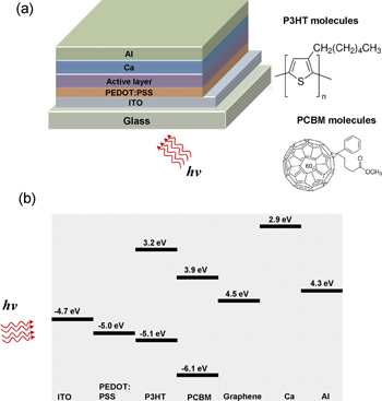
Figure 1. (a) A schematic of the PV heterojunction device structure, and (b) the corresponding energy levels.
Download figure:
Standard image High-resolution imageTypical TEM and SEM micrographs of the P3HT:PCBM:GNP with graphene concentrations of 1, 3 and 5 wt.% are shown in figure 2.
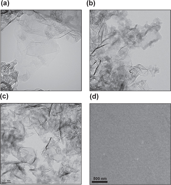
Figure 2. Typical TEM images of the P3HT:PCBM:GNP nanohybrid with a graphene content of (a) 1 wt.%, (b) 3 wt.% and (c) 5 wt.%. (d) Representative SEM micrograph of the nanohybrid in (b).
Download figure:
Standard image High-resolution imageFor 1 and 3 wt.% GNP loading, the obtained films showed good dispersion of single or few graphene sheets (figures 2(a), (b)), while excess doping of 5 wt.% loading caused the stacking of graphene in the active layer (figure 2(c)). A precedent research work [27] established that the inter-chain interaction, crystallization and phase separation of the photoactive layers are dependent on the composite blend and the GNP concentration.
Figure 3 displays the typical microRaman spectra of the active layer components, namely graphene and P3HT:PCBM. The Raman spectra of graphene exhibit a typical shape identified by two main modes labeled the G and 2D bands. Other bands are also featured and may also be observed in graphene when structural defects occur within the carbon lattice. These bands supply important information when scrutinized closely. The sharp G band positioned at approximately 1587 cm−1 is due to the in-plane vibrational mode implicating the sp2 hybridized carbon atoms that constitute the GNP sheet. Its location is extremely sensitive to the number of layers constituting the sample and is considered to be one of the most powerful methods to define the layer thickness. The 2D band is known as the second order of the D band, but unlike the D band, it does not represent structural defects. It is the consequence of a two-phonon lattice vibrational mode, and is constantly present as an intense band in the graphene material, even in the absence of the D band. To determine the layer thickness from the 2D band, the band position and band shape can be used. Furthermore, the ratio of the intensities of the 2D band relative to the G band can be used to determine the layer thickness. The Raman spectra shown here are indicative of a graphene sample with an average layer thickness between three and ten layers [45].
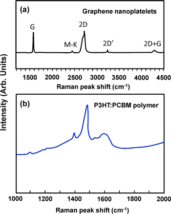
Figure 3. (a) Representative Raman spectra of (a) pure GNP with its associated modes, and (b) a pristine P3HT:PCBM blend.
Download figure:
Standard image High-resolution imageThe PCBM polymer shows Raman peaks at 1355 and 1582 cm−1. The peak located at 1501 cm−1 corresponds to the C60 at PCBM [46]. For the P3HT:PCBM composite film, the Raman shift peaks observed at 1377, 1449, 1490 and 1600 cm−1 correspond to the P3HT and PCBM materials.
To investigate the crystalline quality of our films, we employed GAXRD analysis on pristine P3HT:PCBM with different GNP content. Figure 4 shows the XRD profile (θ–2θ) of the P3HT:PCBM and P3HT:PCBM:GNP with different content. For the as-deposited P3HT:PCBM spectrum, a broad peak at 22o is observed due to PCBM, which depicts its amorphous nature, whereas a sharp peak is observed at 5.37o (2θ value) due to the reflection plane (100) (edge-on orientation) of the thiophene rings in a P3HT chain. P3HT has the ability to crystallize and has a stabilizing effect on blend morphology [47]. After annealing at 110 oC, crystalline P3HT becomes interconnected with amorphous PCBM and (200) and (300) diffraction peaks appear as well. A smaller 'd' spacing for the P3HT:PCBM blend may facilitate the intermolecular transfer of charge carriers in the film. A weak (001) peak related to the GNP was observed at low concentration (1 wt.%), while a more intense (002) one appears clearly starting from 3 wt.% and above (i.e. 5 wt.%) suggesting an improvement of the crystalline quality of the whole blend. This may lead to more intermolecular charge carrier transfers in the P3HT:PCBM:GNP layer. The existence of GNP nanostructures in the blend is hence confirmed by the peaks observed at 26.5o and corresponds to the (002) plane.
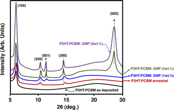
Figure 4. The GAXRD pattern of the as-deposited and annealed P3HT:PCBM blend and P3HT:PCBM:GNP thin films with 1, 3 and 5 wt.% of GNP; (*) labels the GNP peaks.
Download figure:
Standard image High-resolution imagePhotoluminescence (PL) spectroscopy is an effective tool to establish the charge transfer at the donor/acceptor interface [48]. Figure 5(a) shows the PL spectra of the photoactive layer corresponding to different graphene loading. The PL was obtained using 355 nm as the excitation wavelength. We observe that the addition of graphene produces clear quenching of the PL spectra, supporting an interaction between P3HT:PCBM and graphene, on the one hand, and an electron transfer from the conjugated polymer to the graphene on the other. We suggest that this increase in electron transfer with respect to graphene loading is due to the improvement of the charge dissociation in the P3HT:PCBM:GNP interface area, and the increase in the number of available electron paths. Similarly, Su and co-workers [49] demonstrated that π-interactions between donor and acceptor molecules and the graphene basal plane are responsible for the charge-transfer at their interfaces [49].
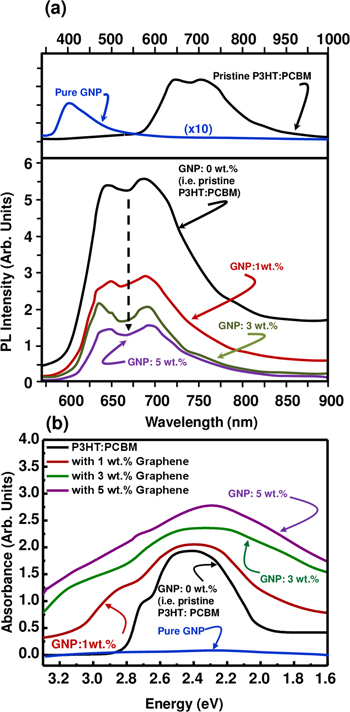
Figure 5. Typical (a) photoluminescence intensity and (b) light absorbance of P3HT: PCBM:GNP nanohybrid at 0, 1, 3, and 5 wt.% graphene loading. The inset in (a) shows the PL of the pristine P3HT: PCBM and the pure GNP in DI water.
Download figure:
Standard image High-resolution imageThe PL of the GNP alone shows a weak near-UV blue emission centered at around 400 nm. This weak near-UV blue emission in the GNP films has been reported earlier in reduced GO [50]. The PL response could be due to the binary recombination of electron–hole pairs localized within sp2 carbon. Although the mechanism of light emission from GNP has not been fully explored yet, we believe that the PL spectra in GNP also depend on the size, shape and fractions of the graphitic regions (sp2 domains) and possible oxidized regions (sp3 domains) that may occur during manipulation with various solvents [51].
Photon absorption measurements were performed in the visible range, i.e. 1.6 to 3.3 eV, and are displayed in figure 5(b). The UV–vis spectrum of the pure GNP shows a flat curve, while the presence of P3HT and PCBM in the active layer was confirmed again using UV–vis spectroscopy. The P3HT:PCBM blend shows maximum absorption at 2.4 eV (550 nm) along with a shoulder peak at 2.7 eV. The prominent peak located at 2.4 eV (for 0 wt.% of GNP, i.e. pristine P3HT:PCBM) is due to C60 fullerene acceptors that improve the π–π stacking of the P3HT polymer chains, while the presence of the shoulder peak at 2.7 eV is attributed to strong inter-chain interactions which are responsible for charge transport efficiency [52]. This spectrum shows a clear red shift when GNP is added. For instance, red shift might be observed due to increased delocalized excitons in the highly π-conjugated P3HT domains.
Similarly, the number of delocalized excitons in P3HT:PCBM may also increase due to a greater amount of molecular interactions when graphene is added [22]. Since GNP is an sp2 hybridized material, it displays π–π molecular interaction that is responsible for the enhancement of delocalized excitons. Accordingly, P3HT:PCBM:GNP features a broader range of light absorption in the visible range and the peak due to the π–π* electronic transitions between the 0 and 1 spin states becomes broader. Therefore, more exciton generation is expected following the absorption of more photons by the photoactive layer [53].
Finally, a solid-state photovoltaic-like device was fabricated on ITO-coated glass substrates (with different graphene loading), as displayed in the schematic of figure 1(a).
As shown in figure 6, the current–voltage (J–V) plot shows clear p–n junction-like behavior when illuminated. The J–V curve shifts downwards, which is the typical diode response expected from the photovoltaic effect. The photovoltaic effect is attributed to the P3HT:PCBM:GNP generating excitons when illuminated.
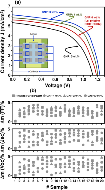
Figure 6. (a) Typical J–V characteristics of polymer P3HT:PCBM:GNP solar cells with 0, 1, 3 and 5 wt.% graphene loading, and (b) device-to-device variation for each measured performance (Voc, Jsc and FF) for a set of 20 samples. The first measurement is taken as a reference.
Download figure:
Standard image High-resolution imageThe integration of GNP most probably improved the direct contact between the nanohybrid components by increasing the interface that helps photogenerated exciton dissociation and promotes electron transport in the conjugated polymer. Moreover, the electrically conductive GNP allows direct pathways for the conduction band electron transportation to the Al electrodes.
Table 1 shows the electronic and photovoltaic characteristic parameters of solid-state devices based on P3HT:PCBM:GNP films with various graphene concentrations.
Table 1. Electronic and PV performance of the P3HT:PCBM:GNP composites.
| Graphene wt.% | Hall mobility (cm2 V.s–1) | JSC (mA cm–2) | VOC (V) | FF (%) | η (%) |
|---|---|---|---|---|---|
| 0 | 4.62 × 10⁻⁵ | 5.61 | 1.19 | 38.04 | 2.54 |
| 1 | 6.46 × 10⁻⁴ | 5.79 | 1.22 | 42.18 | 2.98 |
| 3 | 9.12 × 10⁻⁴ | 6.18 | 1.24 | 47.12 | 3.61 |
| 5 | 1.01 × 10⁻³ | 5.41 | 1.14 | 33.23 | 2.05 |
We have calculated the charge carrier mobility of holes and electrons by using electron-only and hole-only devices through space-charge-limited fabricated devices using appropriate Au electrodes (for the hole) and Al (for the electrons). We then estimated the hole and electron mobilities of pristine and GNP-doped films of P3HT:PCBM by the Mott–Gurney law [54]:

where J is the current density, ε is the dielectric constant of the medium, μ is the carrier mobility and L is the thickness of the film. The values of the mobility for freshly prepared devices are listed in table 2. It can be seen that both the electron and hole mobilities are significantly affected by the addition of GNP, which is expected as the graphene aids the transportation of charges by offering new interfaces for carrier dissociation and improves the overall electrical conductivity of the blend. In other words, the GNP facilitates the charge transfer through the photoactive layer. This may also be interpreted in terms of the band diagram shown in figure 1. The energy level of the GNP lies between P3HT:PCBM and PEDOT:PSS, providing a favorable path for both electron and holes to reach the electrode. This also explains the increase in current density observed in the GNP-doped devices. We also note that the electron mobilities calculated through the Mott–Gurney law corroborate those estimated by the Hall effect very well within experimental uncertainties.
Table 2. A summary of the calculated hole and electron mobilities of the pristine P3HT:PCBM and P3HT:PCBM with 1, 3 and 5 wt.% of GNP.
| Sample | Hole mobility (cm2 Vs–1) | Electron mobility (cm2 Vs–1) | Device-to-device fluctuation (20 samples) |
|---|---|---|---|
| P3HT:PCBM | 2.57 × 10⁻⁶ | 4.01 × 10⁻⁵ | 3.6% |
| P3HT:PCBM + 1 wt.% GNP | 3.11 × 10⁻⁵ | 5.77 × 10⁻⁴ | 2.5% |
| P3HT:PCBM + 3 wt.% GNP | 4.09 × 10⁻⁵ | 1.48 × 10⁻³ | 4.9% |
| P3HT:PCBM + 5 wt.% GNP | 6.03 × 10⁻⁴ | 1.16 × 10⁻³ | 2.8% |
The PV power conversion efficiency η is defined by:

and the fill factor (FF) is described by

where Iinc is the incident optical power density of the lamp, which is measured to be 100 mW cm−2. Vmax and Imax are the voltage and current at the maximum power point, respectively.
Besides the PCE, polymer-based OPVs can be evaluated by using three other key parameters: Jsc, Voc and FF. These parameters are inherently related to device structure, material properties and interface effects. Equation (1) describes the relationship between these parameters and the cell efficiency.
Some recombination processes may govern the characteristic solar cell parameters. Jsc and Voc are primarily influenced by the energy band profile of the absorbing active layer. While the losses in Jsc are presumably the result of poor transport and can be improved through the polymer planarity, both Voc and Jsc are dependent on the intermolecular energy transfer. The recombination of charge carriers at the D/A interface is detrimental to the Voc. The lower band gap of the donors D leads to the higher Jsc current and improved band alignment of the acceptors (A) leads to a higher Voc.
On the other hand, the fill factor (FF), is related to the efficiency of charge extraction/collection or charge transfer efficiency between different layers of the OPV device, and is affected by the photocharge carrier mobility and recombination rates.
As described in table 1, a 3 wt.% addition of graphene to the photoactive layer results in an increase in Voc from 1.19 to 1.24 V and Jsc from 5.61 to 6.18 mA cm−2. Hall mobility was found to increase proportionally to the graphene loading due to the increase in the carrier concentration and the electrical conductivity.
Here, the increase in Jsc is attributed to the improvement of the charge collection efficiency and the transport of electrons, leading thereby to a lowering of the exciton recombination rate and the augmentation of the free carrier lifetime. The PCE (η) value of the OPV devices increases from 2.54% to 3.61%. The value of Voc, associated with the GNP content of the mixture, is also impacted by the electrode work function. Consequently, when the load of GNP exceeds 3 wt.%, η diminishes due to an increase in leakage current [55]. Moreover, beyond the intrinsic electrical properties of the GNP itself, it has to be highlighted that the improvement of the electronic and the photovoltaic properties, especially with low GNP loads, can also be attributed to the possible alignment of graphene flakes, which in turn is influenced by the graphene concentration, density and the interaction with the conjugated polymer.
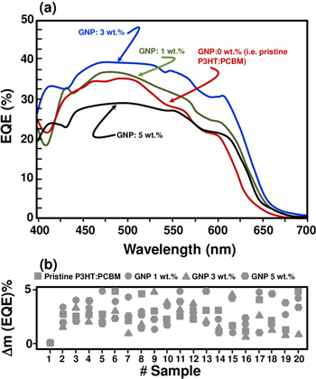
The EQE spectra of the OPV device-based P3HT:PCBM and P3HT:PCBM:GNP are displayed in figure 7. Even though all the spectra somehow show similar behavior, devices containing 3 wt.% of GNP show the highest EQE values for almost all the spectrum wavelengths. In fact, given the same wavelength, for example at 470 nm, the EQE maximum is 35% for the 0% GNP (i.e. pristine P3HT:PCBM) device, while it is 37.5% and 39.5% for 1 and 3 wt.% of GNP integration, respectively. This difference is likely due to the improved efficiency of the collection of electrons in the OPVs. As shown in figures 6(b) and 7(b), these results were highly reproducible within the experimental uncertainties, which were about 5% (i.e. device to device fluctuation) and measurements were provided over 20 different samples for each load.
Figure 7. (a) A typical EQE spectrum of polymer P3HT:PCBM:GNP solar cells with 0, 1, 3, and 5 wt.% graphene loading. (b) Device-to- device variation for a set of 20 samples. The first measurement is taken as a reference.
Download figure:
Standard image High-resolution image
In sum, there is indeed a competition phenomenon: the decrease in PV performance for 5 wt.% of GNP is interpreted by the increase of leakage current, which corroborates the other results well. Indeed, a similar trend in current density and open circuit voltage is observed in all devices, i.e. an increase with GNP concentrations followed by a decrease at higher amounts of 5 wt.%, which may have led to the formation of shorting pathways. As a matter of fact, attempts to avoid shorting have been made by Mallajosyula et al [56]. They introduced an additional layer of P3HT:PCBM between PEDOT:PSS and the active layer to avoid such a shorting.
These observations clearly indicate that optimization of the active layer and/or processing steps is an important factor every time a new material is incorporated in the blend. Furthermore, the concentration of GNP in the P3HT:PCBM blend, the orientation of the graphene flakes together with their aspect ratio could also influence the optoelectronic properties of the photoactive layer, so a definite conclusion cannot be drawn as to whether GNP doping influences the overall performance by itself or not. Moreover, the closely packed morphology of the P3HT:PCBM blend may have been disrupted by the presence of GNP, causing a change in the highest occupied molecular orbital and lowest unoccupied molecular orbital (HOMO-LUMO) gap. The GNP can hence modify the electronic structure, because the more light is absorbed, the more photons are harvested.
Finally, the reported efficiency values are definitely below the optimal values, as the photogenerated current is relatively low and the energy barrier between the active layer and the PEDOT:PSS is rather large. This performance will surely be ameliorated by optimizing the device structure.
4. Conclusions
Graphene nanoplatelets were integrated at different concentrations into a P3HT:PCBM conjugated polymer matrix to build an organic heterojunction photovoltaic device. MicroRaman spectroscopy, photoluminescence and optical absorbance were employed to systematically investigate performance with respect to GNP loading. Furthermore, these nanohybrids manifested clear PL intensity quenching. We suggested that photo-excited charges were transferred from the P3HT polymer to the existing electronic empty states of the GNP. Once integrated into a solid state OPV device using PEDOT:PSS on an ITO/glass substrate, the nanohybrids show a typical J–V curve shift, characterizing PV behavior. GNP integration was found to increase the Jsc in these OPVs. The best efficiency was 3.61, obtained with 3 wt.% of graphene. Graphene integration definitely improves the donor/acceptor balance at the interface. This enhances the capacity of the separation of the generated photo-charge and decreases the charge transfer paths by offering multiple pathways, which enhances the Jsc density and the PCE in runs. Our study helps to open the way for the application of graphene in OPVs and indicates that such nanohybrids could be efficiently applied to solid state optoelectronic devices.
Acknowledgments
We acknowledge funding from the Qatar Environment and Energy Research Institute (QEERI, Seed Project S-1502), at Hamad Bin Khalifa University, member of Qatar Foundation, the Natural Science and Engineering Research Council (NSERC) of Canada for a Collaborative Research and Development Project in partnership with Raymor Ind. Inc. and the Quebec Prompt Financing ICT R&D program.
Conflict of Interest
The authors declare that they have no conflict of interest.