

Abstract
There is significant interest in the growth of single crystal monolayer and few-layer films of transition metal dichalcogenides (TMD) and other 2D materials for scientific exploration and potential applications in optics, electronics, sensing, catalysis and others. The characterization of these materials is crucial in determining the properties and hence the applications. The ultra-thin nature of 2D layers presents a challenge to the use of x-ray diffraction (XRD) analysis with conventional Bragg–Brentano geometry in analyzing the crystallinity and epitaxial orientation of 2D films. To circumvent this problem, we demonstrate the use of in-plane XRD employing lab scale equipment which uses a standard Cu x-ray tube for the analysis of the crystallinity of TMD monolayer and few-layer films. The applicability of this technique is demonstrated in several examples for WSe2 and WS2 films grown by chemical vapor deposition on single crystal substrates. In-plane XRD was used to determine the epitaxial relation of WSe2 grown on c-plane sapphire and on SiC with an epitaxial graphene interlayer. The evolution of the crystal structure orientation of WS2 films on sapphire as a function of growth temperature was also examined. Finally, the epitaxial relation of a WS2/WSe2 vertical heterostructure deposited on sapphire substrate was determined. We observed that WSe2 grows epitaxially on both substrates employed in this work under all conditions studied while WS2 exhibits various preferred orientations on sapphire substrate which are temperature dependent. In contrast to the sapphire substrate, WS2 deposited on WSe2 exhibits only one preferred orientation which may provide a route to better control the orientation and crystal quality of WS2. In the case of epitaxial graphene on SiC, no graphene-related peaks were observed in in-plane XRD while its presence was confirmed using Raman spectroscopy. This demonstrates the limitation of the in-plane XRD technique for characterizing low electron density materials.
Export citation and abstract BibTeX RIS
1. Introduction
2D materials have attracted increasing attention in different fields of science due to their appealing properties. These include direct to indirect bandgap transition from monolayer to bulk accompanied by the narrowing of the bandgap for W and Mo dichalcogenides, superconductivity in Nb, V and Ta dichalcogenides, semimetals and metallic and paramagnetic behaviors in Pt and Pd dichalcogenides [1]. A variety of 2D material systems have been synthesized including transition metal dichalcogenides (TMD) (e.g. WS2, WSe2, MoS2, MoSe2, NbS2) sp2-BN, black phosphorus and others using various synthesis methods. One of the more promising methods is gas source chemical vapor deposition (CVD) that has been shown to be capable of producing uniform, coalesced large scale films [2–9]. For the assessment of the quality of the deposited films, common characterization techniques include Raman spectroscopy, atomic force microscopy (AFM), x-ray photoelectron spectroscopy, photoluminescence spectroscopy, transmission electron microscopy (TEM) combined with electron diffraction (ED) as well as charge carrier transport properties probed on field effect devices fabricated from 2D materials [10–14].
Another important aspect of 2D film growth using vapor deposition techniques such as CVD, physical vapor deposition, molecular beam epitaxy, atomic layer deposition and others that is usually not well addressed is the orientation of the crystal with respect to the substrate. To some extent, this can be assessed by ED techniques like ED in TEM, reflection high energy ED (RHEED) and low energy ED (LEED) however these are limited to a small volume being probed. In the case of individual domains such as the triangular domains common for TMD films, the orientation of the film with respect to the substrate can be addressed from visual evaluation of the orientation of characteristic triangular features on the surface using microscopy techniques (AFM, SEM, optical microscopy). In this approach, the orientation of the substrate must be known (e.g. primary flat of the wafer) and an assumption of which lattice plane the triangle edge is parallel to must be made. This technique is indirect and therefore requires additional characterization in order to be confirmed. Diffraction techniques like RHEED and LEED can give information on the epitaxial relation of the film with respect to the substrate by observing the crystal structure in reciprocal space and are capable of mapping crystal orientation over the substrate to give an overview of the crystallinity over the whole wafer [15–17]. In the case of TEM, the film is usually removed from the substrate to perform plan-view analysis which is destructive and also eliminates the link to the substrate since the film is removed from the wafer [18, 19].
Determining the epitaxial relation of the 2D material with respect to the substrate is important whether there is any degree of orientation or the film has a fiber structure (oriented out-of-plane with no in-plane orientation). In the case of a single phase film, the presence or lack of epitaxial relation or even various epitaxial relations within a polycrystalline film could affect transport properties as different domain orientations will merge forming grain boundaries. The same will be true for multiphase in-plane heterojunctions. In the case of vertical stacking of 2D layers, the relative rotation between adjacent layers is of interest since it determines band alignment that has been shown to affect transport properties in two-layer graphene and interlayer exciton emission intensities and energies in TMD heterostructures [20–22].
For the determination of the epitaxial relation in classical '3D' thin films, the technique of choice is x-ray diffraction (XRD) pole figure measurements. This technique is nondestructive (if there are no chemical reactions happening under x-ray illumination), usually does not require sample preparation and is fast (result can be obtained in less than an hour). In this technique, an {hkl} plane family with h and/or k and l not equal to zero is probed for both film and substrate to determine crystallographic orientation. For 2D materials there is no continuity of the film along the [000l] direction meaning that pole figure measurements will not give any result. On the other hand, there is still continuity (periodicity) within the (0001) plane. This means that (hki0) planes are still present in the crystal and can be assessed by diffraction techniques as is done in RHEED, LEED and ED in TEM. Thus, for the TMD where both constituents have high electron density, lab scale XRD performed with the x-ray incidence plane nearly coinciding with the sample surface plane (an offset angle that is higher than the x-ray total external reflection angle) should be able to determine the in-plane epitaxial relation between the film and the substrate. Synchrotron based XRD has been widely implemented for analysis of surface reconstruction and monolayer materials orientation and crystallinity due to the high intensity of the beam compared to x-ray tube produced radiation (3–10 orders of magnitude higher spectral brightness), but it is difficult to employ for routine analysis [23, 24]. Synchrotron grazing-incidence wide-angle x-ray scattering (GIWAXS) has been implemented for the analysis of MoS2 orientation with respect to the SiC substrate with a graphene interlayer where the orientation of all crystals has been determined through the observation of peaks resulting from diffraction from  planes of MoS2, graphene and SiC [25]. The authors determined the epitaxial relation, estimated the width of the peaks and calculated the in-plane lattice parameters of all crystals [25]. Similar analysis can be conducted using in-plane XRD where the width of the peak can be estimated in both 2θ and ϕ (same as ω in in-plane configuration) and lattice parameters can be derived.
In this paper, we demonstrate the feasibility of using lab scale (non-synchrotron) XRD instrumentation for in-plane XRD measurements of 2D monolayers and few-layer films that is often assumed to be impossible due to the lack of periodicity in the third dimension. While there is no crystal periodicity out-of-plane, the in-plane component is present and has been probed by implementing XRD θ–2θ and ϕ measurements in the in-plane geometry, to observe the presence of the reciprocal space points and their distribution, respectively. This technique can be employed for the determination of the epitaxial relation of the film and heterostructure components with respect to the substrate, crystal orientation distribution if several present, presence of different crystal phases as well as alloy formation and composition.
2. Experimental
A PANalytical MRD diffractometer with 5-axis cradle was employed for XRD characterization of 2D films. A standard Cu anode x-ray tube operated at 45 kV accelerating voltage and 40 mA filament current was used to generate x-rays. Different configurations of the incident beam and diffracted beam optics were employed. Since a collimated beam with high intensity is required to achieve detectable signal from the thin 2D film and avoid peak broadening due to the sample height variation (sample length along scattering vector) acceptable optics on the incident beam side are capillary optics (x-ray lens), x-ray mirror (parabolic mirror) and hybrid mirror (2-bounce monochromator combined with a parabolic mirror). The same requirements are valid for the diffracted beam side. These requirements lead to the choice of 0.27° parallel plate collimator and 0.04 rad Soller slit combined with either PIXcell or Xenon detector.
The choice of a hybrid mirror over other mentioned optics is beneficial to discriminate Cu Kβ and Kα2 radiation from the incident beam. In the other two configurations, Cu Kβ should be removed employing a Ni filter while Kα2 will be still present. If the presence of Cu Kα2 is not considered to be a problem, an x-ray lens and mirror would lead to higher intensity of the incident beam, improving sensitivity. Otherwise, if higher resolution is required, a hybrid mirror is a better choice. A 4-bounce x-ray monochromator is not considered in this study as it gives only a small fraction of the intensity present in the initial beam and detection of the peaks from the 2D film is expected to be impossible with this type of optics. On the other hand, an x-ray lens was not tested either since both a mirror and hybrid mirror gave sufficient results for the analysis. Nonetheless, an x-ray lens is expected to provide the same information as a mirror.
To perform in-plane diffraction, the x-ray incidence plane was adjusted to nearly coincide with a sample surface plane. 'Nearly' in this case is determined by the x-ray total external reflection angle which is materials dependent and usually below 1° from the surface to the beam. Figure 1 shows illustrations of the Bragg–Brentano measurement geometry (figure 1(a)) where the x-ray scattering vector Q (Q = k1 – k0) is normal to the sample surface (parallel to surface normal n) and in-plane measurement geometry illustrations from two sides (figures 1(b) and (c)). In this illustration, k0 and k1 are the incident and diffracted beams, respectively. Angle ω is an angle between incident beam k0 and a vector that defines the intersection line between the sample surface and the x-ray incidence planes. In Bragg–Brentano geometry, this angle is well defined while in in-plane diffraction this angle coincides with the angle ϕ that defines the rotation of the sample around its surface normal n. Angle χ is defined as an angle between the surface normal n and the x-ray incidence plane. 2θ angle is an angle between incident k0 and diffracted k1 beams.
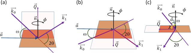
Figure 1. (a) Bragg–Brentano measurement geometry. (b) and (c) in-plane measurement geometry from two perspectives.
Download figure:
Standard image High-resolution imageInitial instrument alignment was performed according to the standard procedure starting with 2θ alignment, coarse height alignment to get about half of direct beam intensity followed by tilt alignment and more fine height alignment to get half of direct beam intensity. Further, the sample was tilted to a χ angle of 88°, 2θ angle was set to the (hki0) plane of the substrate and a ϕ scan was performed for the ϕ alignment. When the position of a peak in ϕ was determined, 2θ and χ alignment was performed. The ϕ, 2θ and χ alignment was conducted to obtain the highest peak intensity. Next, the goniometer was set to the (hki0) plane peak position of the material under consideration and a ϕ scan was performed. Similarly to the substrate peak, χ and 2θ alignment were performed for the film peaks. After this alignment procedure, ϕ and 2θ scans were recorded for both substrate and film. From the performed measurements, it is straightforward to determine the epitaxial relation of the film with respect to the substrate. This technique is able to determine whether or not a preferred orientation is present and provide information on the ratio between different orientations in a sample from the intensity of the peaks as well as it does allow for relative comparison between samples. Further quantification is complicated due to the low intensity and low resolution optics used. In addition, this technique does not allow characterization of films on the surface of the substrate when the films exhibit a fiber structure due to the spread of the diffraction peak intensity in ϕ into a 360° angle.
Samples were prepared employing a horizontal cold-wall CVD reactor using tungsten hexacarbonyl (W(CO)6) and hydrogen chalcogenides (H2S or H2Se) as tungsten and chalcogen precursors, respectively. Two inch diameter c-plane sapphire ((0001) α-Al2O3) wafers were used as substrates for the deposition of WS2, WSe2 and WSe2/WS2. In addition, 1 × 1 cm2 (0001) Si-face 6H-SiC with epitaxial graphene formed by Si sublimation at high temperature was used as the substrate for WSe2 deposition. Hydrogen was used as the carrier gas during deposition and the total pressure in the reactor during deposition was 200 Torr for WSe2 and 50 Torr for WS2 film growth. The growth temperatures for WSe2 and WS2 on (0001) α-Al2O3 were 850 °C and 750 °C–1000 °C, respectively. Growth of WSe2 on graphene/6H-SiC was conducted in a smaller scale vertical cold-wall CVD reactor using H2 as carrier gas and tungsten hexacarbonyl with hydrogen selenide as precursors as described elsewhere [8]. A Bruker Icon AFM with Scanassist tips was used to characterize the surface morphology employing Gwyddion software for image analysis [26]. Raman measurements were conducted using HORIBA LabRAM HR Evolution Raman microscope with a laser wavelength of 532 nm to reveal presence of graphene interlayer.
3. Results and discussion
3.1. WSe2 on (0001) α-Al2O3
XRD analysis of WSe2 on 2' diameter (0001) α-Al2O3 was carried out on a sample which was uniformly covered with isolated monolayer and bilayer islands (figures 1(a) and (b)). A θ–2θ scan performed in Bragg–Brentano geometry showed a broad, low intensity peak (figure 2(c)) corresponding to the {0002} plane family of WSe2. A single layer of WSe2 is expected to result in a broad peak with low intensity due to lack of periodicity in the [0001] direction, however, it is insufficient to distinguish between monolayer and few layer films. The θ–2θ scan recorded in the in-plane diffraction geometry at a ϕ angle where the  peak of α-Al2O3 was observed, revealed the presence of both WSe2 and substrate 11
 0 peaks (figure 2(d)). Rotation around the surface normal fixing 2θ angle at the
  peaks of WSe2 and α-Al2O3 shows epitaxial growth with an in-plane epitaxial relation of
  WSe2 ∥
  α-Al2O3 (figure 2(e)). The AFM images (figures 2(a) and (b)) show two families of triangles pointing in the opposite direction which implies the formation of twins with 60° rotation between them. The observed morphology of the film is in line with the XRD observation while the twins present in WSe2 could not be distinguished in the XRD studies due to the 6-fold symmetry of the WSe2 crystal structure.
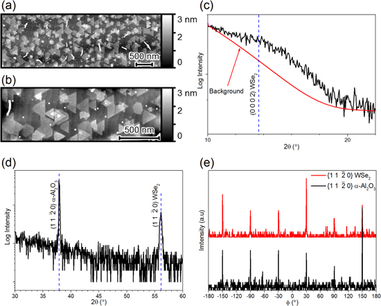
Figure 2. AFM images of WSe2 surface recorded at different magnifications (a) and (b) and XRD diffractogram recorded in Bragg–Brentano geometry (c), in-plane XRD θ−2θ diffractogram (d) and in-plane XRD ϕ-scan of {11 0} planes of WSe2 and α-Al2O3 (e) red and black curve respectively.
Download figure:
Standard image High-resolution image3.2. WS2 orientation evolution with growth temperature
WS2 samples were deposited on 2'' diameter (0001) α-Al2O3 over the temperature range from 750 °C to 1000 °C keeping other deposition parameters the same. The resulting films were expected to be thicker than a monolayer in order to enhance the signal in in-plane XRD measurements. Figure 3 shows the XRD ϕ-scans of  planes of WS2 recorded in in-plane geometry as well as XRD ϕ-scan of α-Al2O3
  recorded in in-plane geometry for the reference. This figure shows the evolution of WS2 crystal orientations in-plane as a function of the growth temperature. At low deposition temperature, WS2 shows two preferred orientations seen from peaks appearing at 0° and 30° in ϕ. These peaks are broad and equal in intensity showing poor alignment of the crystals and equal probability for two orientations. The peak located at 30° in the ϕ-scan shows complex behavior. First, its intensity increases compared to other orientations as the growth temperature is increased from 750 °C to 800 °C followed by broadening of the peak at 850 °C and splitting into two peaks as the temperature is raised to 900 °C and above. At 950 °C, a considerable increase of the peak intensity at 0° compared to other peaks present in the graph is observed which decreases as the growth temperature is increased to 1000 °C. The separation between the split peaks is 4.2° in ϕ and is symmetric with respect to 30°. In addition to these, two other orientations emerge at 900 °C at 19° and 41° in ϕ. Thus, at temperatures of 900 °C and higher there are 5 preferred crystal orientations at 0°, 19°, 27.9°, 32.1° and 41° in ϕ-scan. All these orientations are expected to exhibit anti-phases that appear as opposite direction triangles increasing the total number of preferred orientations to 10. This observation suggests that there are two energetically favorable crystal orientations at the lower temperatures investigated here, but also other orientations are present which become possible at higher temperatures such as those at 19° and 41° and others that become more energetically favorable like orientations at 27.9° and 32.1°. The last two are expected to be more favorable at higher temperatures than 30° as the splitting occurs and is visualized in figure 3 for temperatures of 900 °C and higher.
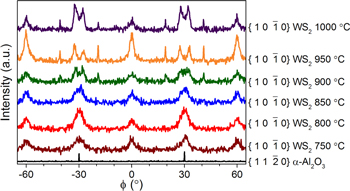
Figure 3. ϕ-scan of 10 0 peaks of WSe2 deposited at different temperatures (colored upper 6 curves) and ϕ-scan of
  peak of α-Al2O3 (black bottom curve) for determination of in-plane epitaxial relation.
Download figure:
Standard image High-resolution imageFigure 4 shows the surface morphology of the samples deposited in the temperature range between 750 °C and 1000 °C. This figure shows the changes in WS2 domain size as a function of temperature where at the lower temperature, the domain size is relatively small (grain side length 30–100 nm for 750 °C deposition temperature) with many big particles that are attributed to 3D growth. An increase in the growth temperature leads to an increase in the domain size and decrease of 3D growth (grain size of 120–660 nm for 1000 °C deposition temperature). This growth behavior is expected as at lower temperature, adatoms on the surface would have lower mobility and longer residence time that leads to higher nuclei density. As the growth temperature increases, adatoms gain mobility and residence time is reduced leading to lower nucleation density and larger grain size. Small spots observed in AFM for the deposition temperatures of 900 °C, 950 °C and 1000 °C are believed to be W or W-rich clusters due to the high vapor pressure of sulfur at higher temperatures that leads to its evaporation leaving excess W on the surface. This is due to the fact that deposition parameters, such as the partial pressures of the precursors, were not optimized for the particular deposition temperatures. In addition, as it can be seen, determination of the WS2 crystal orientations distribution from the topographic study is a complex task making XRD the technique of choice for the crystal orientation determination in epitaxially grown 2D crystals.
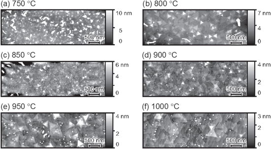
Figure 4. AFM images of the WS2 samples deposited in the temperature range between 750 °C and 1000 °C.
Download figure:
Standard image High-resolution image3.3. WSe2/graphene/SiC
WSe2 was deposited on an epitaxial graphene/6H-SiC substrate using growth conditions which lead to coalesced, primarily monolayer films with some bilayer regions on (0001) α-Al2O3 substrates. Figure 5(a) shows the x-ray diffractogram recorded in Bragg–Brentano geometry showing the region where peaks from the {0002} planes of both WSe2 and graphite are expected. Broad, low intensity features are observed showing formation of WSe2 and graphene on the 6H-SiC which exhibits a forbidden reflection from {0003} planes. Figure 5(b) shows ϕ-scans in a narrow 10° range in ϕ of the  planes of WSe2 and 6H-SiC. This figure (figure 5(b)) suggests the epitaxial relation between 6H-SiC and WSe2 to be {10
 0} WSe2 ∥
  6H-SiC. Although diffraction from the {0002} planes of graphite was observed, there was no in-plane diffraction from the
  planes of graphite (graphene). The later result is expected due to the low electron density of graphite which is critical for the scattering of x-rays. In addition, according to the powder diffraction file for graphite, the intensity of the
  peak in the powder pattern is 7% of the intensity of diffraction from {0002} planes. The percentage in the case of WSe2 for the same planes is 14% in addition to higher relative intensity of the 0002 peak of WSe2 compared to graphite. Thus, this technique is not applicable for characterization of graphene using lab scale equipment and requires a higher intensity x-ray source (e.g. synchrotron). While the presence of the graphene is observed by XRD, its orientation with respect to the 6H-SiC substrate is unknown from the performed measurements.
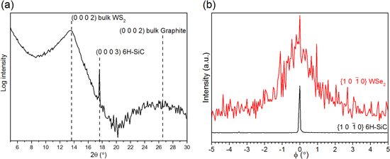
Figure 5. (a) X-ray diffractogram recorded in Bragg–Brentano geometry around 2θ angles of 0002 peaks of WS2 and graphene. (b) ϕ-scan recorded in in-plane geometry showing  peaks of WS2 and 6H-SiC substrate.
Download figure:
Standard image High-resolution imageFigure 6(a) shows the AFM image of the sample surface and (b) the Raman spectra showing the presence of the graphite modes. According to the AFM image (figure 6(a)), the sample is well oriented with respect to the substrate, in accordance with the XRD results, showing two triangle sets pointing in the opposite directions (antiphases with 60° rotation between them). The observation of the graphite G and 2D modes in the Raman spectrum (figure 6(b)) suggests formation of graphene on the surface and the intensity ratio of these two peaks and 2D peak shape and position suggest the formation of non-uniform thickness multilayer graphene on 6H-SiC [27].
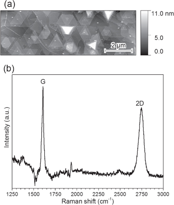
Figure 6. (a) AFM of the WSe2/graphene/6H-SiC and (b) Raman spectrum of the graphene-related region.
Download figure:
Standard image High-resolution image3.4. WS2 on WSe2
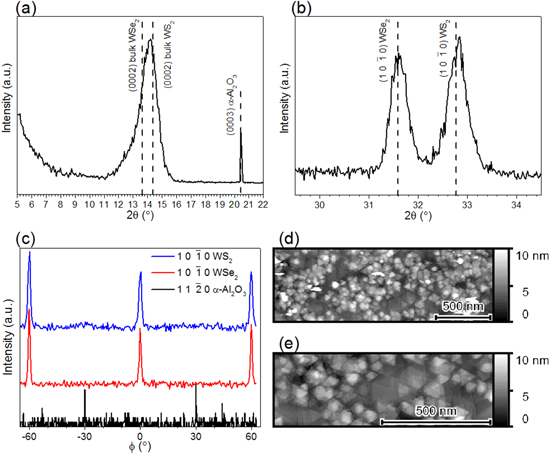
A WS2/WSe2 heterostructure sample was formed by deposition of WSe2 on (0001) α-Al2O3 at its respective growth conditions followed by transition to WS2 deposition at 950 °C and its corresponding growth conditions. The deposition time for each component was prolonged in order to achieve a fully coalesced WSe2 layer and thick WS2 layer in order to increase sampling volume for in-plane XRD. Figure 7(a) shows the θ–2θ x-ray diffractogram recorded in Bragg–Brentano geometry where a high intensity broad peak is observed. It is positioned in between the 0002 peak positions of bulk WSe2 and WS2 suggesting the presence of these materials (or an alloy) and larger layer thickness (high intensity) compared to the prior samples that were studied. XRD θ–2θ scan performed in in-plane geometry, (figure 7(b)), shows well separated peaks of WSe2 and WS2 confirming the presence of both materials with no detectable amount of W(Se, S)2 alloy formation. Figure 7(c) shows ϕ-scans of the  planes of WSe2 and WS2 and also ϕ-scan of the
  planes of α-Al2O3 for determination of the epitaxial relation. The presence of 60° separated peaks of WSe2 and WS2 and the fact that their positions in ϕ coincide suggests the formation of one in-plane crystal orientation with an epitaxial relation as follows:
  WS2 ∥
WS2 ∥  WSe2. The fact that the peaks of the {10
 0} planes of WSe2 and WS2 are 30° rotated from the peaks of
  of α-Al2O3 gives the epitaxial relation of the films with respect to the substrate to be
  WS2 ∥
WS2 ∥  WSe2 ∥
  α-Al2O3. This investigation shows that in-plane XRD can be employed for the determination of the layer orientation in 2D heterostructures. In addition, this measurement shows that WS2 has one preferred orientation when grown on WSe2 compared to growth of WS2 on α-Al2O3 that, as discussed before (figure 3), shows more than one preferred orientation. This could be a key to growth of monocrystalline WS2.
Figure 7. X-ray θ−2θ diffractograms recorded in (a) Bragg–Brentano geometry around 0002 peaks of WSe2 and WS2 and (b) in in-plane geometry around  peaks of WSe2 and WS2. (c) ϕ−scan recorded in in-plane geometry for {10
 0} planes of WSe2 and WS2 as well as for
  planes of α-Al2O3 for determination of epitaxial relation. (d) and (e) AFM images of the WS2/WSe2/α-Al2O3 sample at different magnifications.
Download figure:
Standard image High-resolution image
Figures 7(d) and (e) show the surface morphology of the resulting heterostructure where characteristic triangular features are visible. Larger domains visible in figure 7(e) at the lower level are expected to be multilayer regions of coalesced WSe2 that cover the sapphire surface. The WS2 layer consists of smaller triangular domains that grow preferentially in the vertical direction. This could be an effect of the low sticking coefficient of W and S on the WSe2 surface and together with the selected growth temperature results in a shallower potential well at the step edge of the WS2 domains. This would allow the adatoms to hop on to the top of the WS2 domains and enhance vertical growth. Another explanation of such growth behavior is the difference in the surface energy of the WS2 and WSe2 where if the WS2 has higher surface energy, island growth will be promoted. Two opposite orientations of triangles are present indicating formation of antiphase boundaries that are formed initially in WSe2 and replicated by the WS2. While WSe2 promotes growth of one WS2 orientation, it does not eliminate the formation of antiphases.
4. Conclusions
This work demonstrates that lab scale (non-synchrotron) XRD, using a standard Cu x-ray tube performed in the in-plane geometry can be successfully employed to analyze the crystallinity of ultra-thin 2D films. While it was shown that this technique is suitable for WSe2 and WS2, it was not able to detect diffraction from the graphene  planes. This is expected to be due to the low electron density of carbon atoms that is insufficient for effectively scattering x-rays. As W, Se and S are heavier atoms having higher electron density, the diffraction can be observed without the need for a high intensity x-ray source. As has been mentioned, synchrotron GIWAXS is capable of determining the presence and orientation of the graphene interlayer between the SiC substrate and the MoS2 epitaxial monolayer. This suggests that for the determination of an epitaxial relation of low electron density monolayer films like graphene or boron nitride, synchrotron based x-ray techniques are preferred. Thus we expect this technique to also be suitable for the investigation of other TMD materials. It should be noted that the presented technique is not capable of separating between monolayer and bilayer films and other techniques should be implemented for thickness determination such as Raman spectroscopy or profilometry.
The applicability of the technique to the study of 2D films was demonstrated for several examples including a study of the effect of deposition temperature on the crystallinity of WS2 films deposited on (0001) α-Al2O3, determination of the epitaxial relation of WSe2 on (0001) α-Al2O3 and 6H-SiC with graphene interlayer as well as the epitaxial relation between layers in a WSe2/WS2 vertical heteostructure. The WSe2 was found to be well oriented with respect to the substrates employed in this study but WS2 exhibited several preferred orientations on α-Al2O3 substrate which are dependent on the deposition temperature. In addition, it was shown that WS2 grows epitaxially on WSe2. This underlines the importance of the choice of the substrate even in van der Waals epitaxy where the influence of the substrate is expected to be less pronounced.
Acknowledgments
The work was financially supported by the National Science Foundation (NSF) through the Penn State 2D Crystal Consortium-Materials Innovation Platform (2DCC-MIP) under NSF cooperative agreement DMR-1539916 and the NSF EFRI-2DARE program (Grant EFRI-1433378). MC acknowledges Professor Joshua Robinson for the encouragement to write this article.