

Abstract
In a previous study, we found that hillocks (i.e. surface ion tracks) can be imaged using transmission electron microscopy (TEM) by irradiating thin CeO2 samples with swift heavy ions (SHI) at oblique incidence. In the present study, the same TEM method is applied to Y3Fe5O12 (YIG) and three fluorides (CaF2, SrF2 and BaF2) for observing hillocks. For YIG, which is one of the amorphizable materials, hillocks are found to have amorphous features consistent with amorphous features of ion tracks. For the fluorides, it is found that the hillocks do not exhibit amorphous features, and they are composed of nanocrystallites. Although hillocks for YIG and CaF2 exhibit different crystallographic features, hillock diameter agrees with the molten region diameter predicted by the thermal spike model for both materials. It is found that for YIG the hillock diameter is comparable to the ion track diameter, whereas for the fluorides it is always larger than the ion track diameter. The present result shows the existence of the velocity effect for ion track diameter in CaF2. It is also found that for fluorides both hillock and ion track diameters vary in the order of cation mass (i.e. CaF2 < SrF2 < BaF2). The above results of hillocks and ion tracks for SHI-irradiated fluorides can be consistently interpreted within the framework of the thermal spike model, if melting and successive recrystallization are assumed.
Export citation and abstract BibTeX RIS
1. Introduction
In many ceramic materials irradiated with swift heavy ions (SHI), a continuous damaged region called an ion track is formed along the ion path [1, 2]. Ion track formation has been extensively studied for decades as an important aspect of ion beam induced modification of ceramic materials. When an ion track is formed by SHI irradiation, it is often accompanied by the formation of a hillock (surface ion track) [3–18] which is a protruded part of the ion track. Since the hillock formation process is closely related with that of ion track formation, it is important to compare features of hillocks and those of ion tracks for comprehensive understanding of these modification processes. Therefore, a precise measurement of hillock size is indispensable for elucidating the hillock formation process.
Almost all hillock size data have been measured so far by atomic force microscopy (AFM) [3]. Although AFM is suitable for measuring hillock height, it is not suitable for measuring their diameter. Since diameter measurement by AFM is significantly affected by the curvature of the probe tip, most diameter data are subjected to a systematic error of some nanometers [4–8]. Correction of the measured diameter is needed in order to reasonably estimate the accurate value. Although such correction has been attempted in [8] based on the analysis of the height–diameter relationship, validity of the correction has not been fully tested. Accurate measurement of hillock diameter by AFM is still not straightforward, and the AFM data reported so far should be crosschecked by alternative methods.
Although accurate measurement of hillock diameter is difficult, accurate measurement of ion track diameter is possible by the following methods. For example, transmission electron microscopy (TEM) [19, 20], Rutherford backscattering spectroscopy in channeling condition (RBS/C) [21, 22] and small angle x-ray scattering (SAXS) [23, 24] are methods usually adopted for precise measurement of ion track diameter. Among these techniques, TEM is especially useful for characterizing crystallographic features. Although crystal structure of ion tracks has been extensively studied for many materials, crystal structure of hillocks has been studied only for a limited number of materials, such as Gd2Zr2O7 [25], CeO2 [26] and TiO2 [27]. As the review [3] pointed out, the crystal structure of a hillock is still one of the open questions to be answered for many materials.
Based on the above recognition, we have recently proposed a novel method for characterizing crystal structure of hillocks using TEM [26]. Feasibility of the method for characterizing hillocks has been demonstrated for CeO2 irradiated with SHI. In principle, the method is applicable to most ceramic materials. The present method is illustrated in figure 1. The method consists of two procedures: (1) thin TEM samples are irradiated with SHI at oblique incidence; and (2) hillocks created at a side surface of the as-irradiated sample are observed directly by TEM. The detail of the method is explained in [26]. The method allows us to directly observe hillocks by significantly reducing the overlap of the hillock image and unwanted matrix image. It should be emphasized that by using the present method accurate size of hillocks can be measured, and crystal structure of hillocks can be revealed.
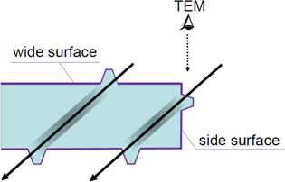
Figure 1. Schematic side view of a thin TEM sample irradiated with SHI at oblique incidence. The solid arrow represents the trajectory of SHI. It shows formation of hillocks and ion tracks. 'Wide surface' represents the front surface or back surface of the sample, while 'side surface' represents the crack face at the side of a thin sample. The direction of TEM observation is indicated by a dotted arrow.
Download figure:
Standard image High-resolution imageIn the present study, we have applied the method to Y3Fe5O12 (yttrium iron garnet: YIG) which is a typical amorphizable material. Amorphizable materials are defined as materials in which amorphous ion tracks are created by SHI irradiation. We have also applied the method to three fluorides (CaF2, SrF2 and BaF2) that are categorized as non-amorphizable materials. Non-amorphizable materials are materials in which the crystal structure within a single ion track is not amorphized [28]. Examples of non-amorphizable materials other than the above fluorides are LiF [29], SnO2 [30] and CeO2 [31]. The strong ionic nature of bonding may be responsible for the non-amorphizable character of these materials [28], but the origin is still debatable.
Distinction between these two types of materials is extremely important for elucidating the mechanism of ion track formation [2, 32]. For amorphizable materials, ion track diameter can be predicted based on the thermal spike model using the melting criterion [33], whereas for non-amorphizable materials ion track diameter observed by TEM is smaller than that expected from the prediction based on the same framework [2, 28, 32, 33]. This means that amorphizability of the material is critical for the mechanism of ion track formation. While the thermal spike model is valid for many amorphizable materials, revised versions of the existing models have been proposed to account for the smaller ion tracks of non-amorphizable materials [32–35]. However, the data are still insufficient to settle the controversy related to small ion tracks. Since a hillock is a part of an ion track, characterization of hillocks can be a useful approach to test the validity of the models. In the present study, hillocks are mainly characterized for both amorphizable and non-amorphizable materials in order to comprehensively understand hillock formation and ion track formation.
2. Experiments
Thin samples for TEM observation were prepared before irradiation by the following procedure. The starting material was a powder of Y3Fe5O12 (3N), CaF2 (3N up), SrF2 (2N) and BaF2 (3N) supplied by Kojundo Chemical Laboratory Co., Ltd. These starting materials were finely ground using an agate mortar and pestle. The ground samples were then placed randomly on a 3 mm diameter 200 mesh copper grid covered with holey carbon film. This means the thickness of the samples placed on the grid were not always the same. The samples were subsequently irradiated with 200 MeV Au32+ ions at oblique incidence (45 degrees relative to normal direction) at room temperature in the tandem accelerator at JAEA-Tokai (Japan Atomic Energy Agency, Tokai Research and Development Center). The charge state (32+) was chosen so that the charge of the incident ions was the same as the average value of the equilibrium charge. The samples were irradiated in the fluence range of 5 × 10¹⁰–2 × 10¹¹ ions cm−2. The as-irradiated samples were examined using a transmission electron microscope (TEM, Model 2100 F, JEOL Ltd) operated at 200 kV. The electronic stopping power (Se) was estimated using SRIM-2008 [36, 37].
3. Experimental results
3.1. Hillocks and ion tracks observed for SHI-irradiated Y3Fe5O12
Figure 2(a) shows a bright field image of YIG irradiated with 200 MeV Au at oblique incidence. Ion tracks are imaged as line-like contrasts. Surface protrusions located at the end of ion tracks are imaged as shown in the figure, indicating that the hillock is created at the side surface of the TEM sample. In the present study, hillocks are successfully imaged by TEM for SHI-irradiated YIG, whereas previous TEM studies [19, 38, 39] have never reported surface protrusion of ion tracks (hillocks) for YIG. The hillock image at the side surface is not overlapped with the matrix image, while that at the wide surface is completely overlapped with the matrix image, as shown in the figure. By observing hillocks at the side surface, it is possible to characterize their crystal structure. It is found from figure 2(b) the hillocks for YIG have amorphous features. Figure 3(a) shows fast Fourier transforms (FFTs) obtained from the hillock of figure 2(b). The figure exhibits a diffused ring which indicates the presence of amorphous phase.
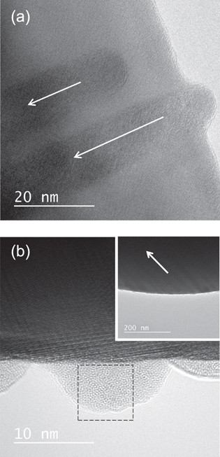
Figure 2. (a) Bright field image of YIG irradiated with 200 MeV Au32+ at oblique incidence. (b) Magnified image of hillocks created at the side surface of YIG irradiated with 200 MeV Au32+ at oblique incidence. The inset shows the low magnification picture of the corresponding image. The direction of the irradiation is indicated by arrows. The area of the hillock image where the FFT image (figure 3(a)) is obtained is indicated as a dotted square.
Download figure:
Standard image High-resolution image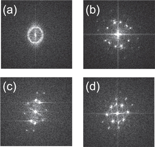
Figure 3. FFT of hillock regions for (a) YIG, (b) CaF2, (c) SrF2 and (d) BaF2. The area of the hillock image where the FFT image is obtained is indicated in corresponding figures (figures 2(b), 5(b), 6(b) and 7(b)).
Download figure:
Standard image High-resolution imageBoth hillock diameter and height located at the side surface can be precisely measured from the TEM picture. The size distributions of hillock diameter and height created at the side surface are shown in figures 4(a) and (b), respectively. The average hillock diameter and height created at side surfaces are Dside = 13.4 ± 1.6 and hside = 5.9 ± 1.0 nm, respectively. Hillocks created at the wide surface are also recognizable as semi-circular black contrasts located at the end of line-like ion track images. The size distribution of hillock diameter at the wide surface (Dwide) is also shown in figure 4(a). The average hillock diameter is Dwide =13.6 ± 1.3 nm, which is almost the same as Dside. Hillock height cannot be estimated from the image of hillocks created at the wide surface, since the hillock image is connected with an ion track image. Therefore, hillock height at the wide surface is not taken into account in this study.
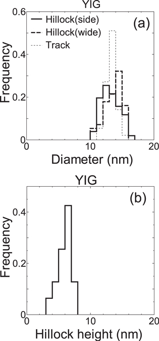
Figure 4. (a) Size distribution of hillock diameter observed at the side surface (Dside) and that of hillocks observed at the wide surface (Dwide) and that of ion tracks (Dtrack) in YIG irradiated with 200 MeV Au32+. (b) Size distribution of hillock height observed at the side surface (hside) in YIG irradiated with 200 MeV Au32+.
Download figure:
Standard image High-resolution imageThe width of line-like black contrast is measured as the ion track diameter. The diameter distribution of ion tracks for YIG irradiated with 200 MeV Au is shown in figure 4(a) together with that of hillocks. The average ion track diameter is estimated to be Dtrack = 13.4 ± 0.9 nm. The figure demonstrates that hillock diameter and ion track diameter are almost the same for YIG. The average sizes of hillocks and ion tracks are summarized in table 1.
Table 1. Average hillock diameter created at the side surface (Dside), average hillock height created at the side surface (hside), average hillock diameter created at the wide surface (Dwide) and average ion track diameter (Dtrack) are listed with standard deviation for YIG, CaF2, SrF2 and BaF2, respectively.
| Dside (nm) | hside (nm) | Dwide (nm) | Dtrack (nm) | |
|---|---|---|---|---|
| YIG | 13.4 ± 1.6 | 5.9 ± 1.0 | 13.6 ± 1.3 | 13.4 ± 0.9 |
| CaF2 | 11.6 ± 1.8 | 8.8 ± 1.5 | 10.8 ± 1.3 | 7.0 ± 1.3 |
| SrF2 | 12.9 ± 2.2 | 9.6 ± 1.8 | 12.4 ± 1.7 | 7.5 ± 1.4 |
| BaF2 | 15.5 ± 2.1 | 11.3 ± 2.5 | 15.2 ± 1.8 | 10.2 ± 1.5 |
3.2. Hillocks and ion tracks observed for SHI-irradiated CaF2, SrF2, and BaF2
Figure 5 shows the bright field image of CaF2 irradiated with 200 MeV Au ions at oblique incidence. In figure 5(a), inhomogeneous ion tracks (white line-like contrasts) are observed. Inhomogeneous features of ion tracks for CaF2 irradiated with 200 MeV Au ions are consistent with the previous result showing the same features of ion tracks created for CaF2 irradiated with a MeV cluster beam [40, 41]. The ion track images are observed clearly when they are observed in off-focus condition. The ion tracks are observed as white contrast with dark fringes when under focused, whereas they turn to black contrast with bright fringes when over focused. Such features of ion track images can be found in other non-amorphizable materials such as in apatite [42, 43], MgAl2O4 [44] and CeO2 [26]. Such Fresnel fringes are indicative of a low-density region formed along the ion path. Although the thickness of the fringe depends on the focus condition, it can be less than 0.5 nm in the present focus condition. The fringe can be the cause of systematic error in ion track diameter measurement. Since the thickness of the fringe is small, the error does not significantly affect the measurement of ion track diameter.
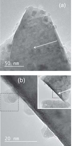
Figure 5. (a) Bright field image of CaF2 irradiated with 200 MeV Au32+ at oblique incidence. (b) Magnified image of hillocks created at the side surface of CaF2 irradiated with 200 MeV Au32+ at oblique incidence. The inset shows the low magnification picture of the corresponding image. The direction of the irradiation is indicated by an arrow. The area of the hillock image where the FFT image (figure 3(b)) is obtained is indicated as a dotted square.
Download figure:
Standard image High-resolution imageNanometer-sized black circular contrasts corresponding to hillocks are observed at both ends of ion tracks. It is recognizable in the figure that some hillocks are created at the side surface.
As shown in figure 5(b), the whole volume of hillocks created for CaF2 has a crystal structure which is in contrast to the amorphous features of hillocks created for YIG. It was already known that ion tracks created for SHI-irradiated CaF2 are not amorphized [2, 32], whereas in the present study hillocks are found to have a crystal lattice for CaF2. Figure 3(b) shows FFTs obtained from the hillock at the upper left of figure 5(b). The figure shows diffraction spots, indicating that the hillock has crystalline features. It is interesting to note that the hillocks do not have a uniform lattice structure, and they are composed of small crystallites. The hillock surface is found to be facetted reflecting the crystal orientation of the nanoscrystallite.
As shown in figure 6(a), inhomogeneous ion tracks are observed also for SrF2 irradiated with 200 MeV Au. Hillocks are observed as black contrasts at both ends of the ion tracks. As shown in the figure, some of the hillocks are created at the side surface. As shown in figure 6(b), the hillocks have a crystal lattice. Figure 3(c) supports the crystalline features of hillocks for SrF2. Similar to the hillocks for CaF2, hillocks for SrF2 consist of nanocrystallites.
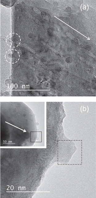
Figure 6. (a) Bright field image of SrF2 sample irradiated with 200 MeV Au32+ at oblique incidence. The dotted circles highlight the hillocks created at the side surface of SrF2 sample. (b) Magnified image of hillocks created at the side surface of SrF2 irradiated with 200 MeV Au32+ at oblique incidence. The inset shows the low magnification picture of the corresponding image. The direction of the irradiation is indicated by an arrow. The area of the hillock image where the FFT image (figure 3(c)) is obtained is indicated as a dotted square.
Download figure:
Standard image High-resolution imageFor BaF2 irradiated with 200 MeV Au, similar to other fluorides, inhomogeneous ion tracks are observed as shown in figure 7(a). In the figure, hillocks are observed at the wide surface of the sample, and they are imaged as black contrasts located at the end of the ion track. As shown in figure 7(b), hillocks can be imaged at the side surface of the BaF2 samples. The whole volume of the hillocks is found to have crystal structure. Figure 3(d) supports the crystalline features of hillocks for BaF2. Similar to other fluorides, the hillocks consist of nanocrystallites with different crystal orientations. Faceting of the hillock surface is also observed, reflecting the crystal orientation of the surface of the hillock.
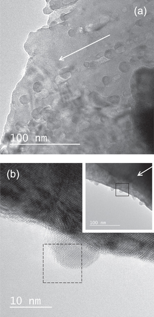
Figure 7. (a) Bright field image of BaF2 sample irradiated with 200 MeV Au32+ at oblique incidence. (b) Magnified image of hillocks created at the side surface of BaF2 irradiated with 200 MeV Au32+ at oblique incidence. The inset shows the low magnification picture of the corresponding image. The direction of the irradiation is indicated by an arrow. The area of the hillock image where the FFT image (figure 3(d)) is obtained is indicated as a dotted square.
Download figure:
Standard image High-resolution imageIn this study, hillock diameter is defined as the maximum width of the hillock image. The size distributions of Dside, Dwide and Dtrack for fluorides are shown in figures 8(a)–(c), respectively. Size distribution of hillock height is shown in figure 9. The average sizes are summarized in table 1. The results demonstrate that Dside is nearly the same as Dwide for all the samples. It is interesting to find that for the three fluorides the hillock diameter increases in the order of cation mass. The size distribution of hillock height (figure 9) also shows a slight increase of hillock height with increasing cation mass.
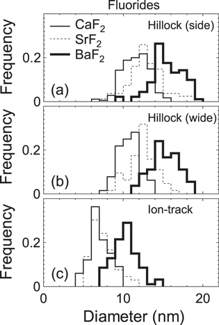
Figure 8. (a) Size distribution of hillock diameter observed at the side surface (Dside) in fluorides irradiated with 200 MeV Au32+. (b) Size distribution of hillock diameter observed at the wide surface (Dwide) in fluorides irradiated with 200 MeV Au32+. (c) Size distribution of ion track diameter (Dtrack) in fluorides irradiated with 200 MeV Au32+.
Download figure:
Standard image High-resolution image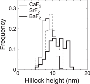
Figure 9. Size distribution of hillock height observed at the side surface (hside) in fluorides irradiated with 200 MeV Au32+.
Download figure:
Standard image High-resolution imageThe present observation enables us to examine cation dependence of ion track diameter. In the case of continuous ion tracks, ion track diameter is defined as the average width of the line-like ion track image, while the continuous part of the ion track is measured for diameter measurement in the case of intermittent ion tracks. From figure 8(c), it is found that there is a trend showing the ion track diameter increases with increasing cation mass, although the diameter for CaF2 and that of SrF2 exhibits almost the same size within experimental error.
4. Discussion
4.1. Validity of estimating hillock size by the present method
AFM has enough spatial resolution in terms of hillock height measurement. Therefore, by comparing hillock height measured in the present TEM study (hside) with those previously measured by AFM (hAFM), accuracy of the hillock height measurement by the present method can be tested. In this study, the hillock height for YIG is estimated to be hside = 5.9 ± 1.0 nm for 200 MeV Au irradiation (Se = 32.9 keV nm−1). According to the height–Se relation based on AFM data [45], hAFM is estimated to be around 5.9 nm for the same Se. Therefore, the present data of hside for SHI-irradiated YIG are in accord with the previous AFM data.
It is also interesting to compare hillock diameter at the side surface (Dside) with that obtained by AFM (DAFM). The previous AFM study [45] showed that DAFM is around 20 nm for Se = 32.9 keV nm−1, and therefore DAFM is obviously larger than the present data (Dside = 13.4 ± 1.6 nm). The discrepancy between these two data is attributable to systematic error caused by the curvature of the AFM probe tip [4–8].
For CaF2 irradiated with 200 MeV Au (Se = 24.3 keV nm−1), the hillock height is hside = 8.8 ± 1.5 nm. According to the previous AFM study [8], hAFM for CaF2 is estimated to be 8.2 nm for the same Se. The present result (hside = 8.8 ± 1.5 nm) agrees with the previous AFM result within the experimental error. Therefore, hillock height measurement using the present method is found to be accurate also for CaF2. In the same literature, the hillock diameter is estimated by AFM measurement and subsequently corrected by analyzing hAFM–DAFM correlation. The validity of the correction can be examined by the present study. Although the hillock diameter (Dside = 11.6 ± 1.8 nm) for CaF2 irradiated with 200 MeV Au is close to the hillock diameter corrected after AFM measurement (DAFM = 14.5 ± 3.5 nm) [8], it seems that the present value gives a slightly smaller value than the latter. It should be noted that the hillock diameter corrected after AFM measurement is almost constant irrespective of Se value in the range of Se = 12–35 keV nm−1 [8], although the ion track diameter is known to increase with Se in the range of 8–46 keV nm−1 [32]. Since the present result suggests that hillock diameter is the same as ion track diameter, we believe Se-dependence of hillock diameter should behave in the same way as that of ion track diameter. In this sense, the correction of AFM data of hillock diameter may be insufficient. If this is the case, the possible discrepancy of hillock diameter value between the two methods becomes large especially at lower Se. Such a comparison for the low Se region should be examined in future. Nevertheless, it can be concluded that the present measurement method gives reasonable accuracy for both hillock height and hillock diameter.
Although we have made every effort to rule out partially overlapped hillocks when performing height measurement, there is always a possibility of a small overlap of the hillock image with the matrix image. This means that the measured height data may be smaller than the actual hillock height. The possibility of such partial overlap may affect the credibility of height measurement, and we have to admit that such a problem cannot be solved completely. Nevertheless, it is rather easy to discard partially overlapped hillocks for YIG, since tails of hillock images are recognizable near the side surface as shown in figure 2 when the overlap is negligibly small. Although it is possible that the present method may cause systematic error in height measurement, the comparison between present height data and AFM data has demonstrated that reasonable accuracy can be achieved by the present method of height measurement.
Here, it is also important to take account of nanoscale effects when comparing TEM data and AFM data, since the thickness of TEM samples is typically around 100 nm whereas AFM samples are bulk samples. Melting temperature can have a lower value in nanoscale materials [46]. Such a nanoscale effect may enhance the damage compared with bulk materials. Moreover, it has been reported for germanium that track registration by high energy fission fragments becomes easier for thinner samples when compared with thicker samples [47]. The author of the paper has suggested that it is accountable by the change in thermal conductivity. Such nanoscale effects may enhance the damage compared with bulk materials. Although the above nanoscale effect is possible, we could not detect it. The present result shows agreement of the TEM result with the AFM result.
4.2. Validity of estimating ion track diameter by the present method
In most of the previous studies of ion tracks, irradiations have been done at normal incidence. Therefore, most of the ion tracks have been imaged by TEM as circular contrasts, and in most studies so far ion track diameter has been defined as the diameter of the circular contrasts. In the present study, ion tracks are imaged as line-like contrast, since the samples are irradiated at oblique incidence. In this case, line-like contrast width corresponds to ion track diameter. Here, it is important to test the validity of estimating ion track diameter from the width of line-like contrasts. The present result shows that the width of ion tracks for YIG irradiated with 200 MeV Au (Se = 32.9 keV nm−1) is Dtrack = 13.4 ± 0.9 nm, whereas the previous TEM observation have shown that the diameter of circular contrasts is 13.1–14.2 nm for YIG at the same Se [19]. Therefore, it is found that the present result is consistent with the previous result.
In the previous study of ion tracks in CaF2 irradiated with cluster ions [40], thin TEM samples were irradiated at normal incidence, and the ion track diameter has been estimated from the width of line-like contrast which is imaged by tilting the sample in the TEM machine. Therefore, the method of measuring ion track diameter is basically the same as the present method. In the same literature, ion track diameter is estimated to be 6.1 and 10.9 nm for Se = 14.7 and 47.2 keV nm−1, respectively. Therefore, the present data (Dtrack = 7.0 ±1.3 nm for Se = 24.3 keV nm−1) are consistent with the previous result. It is important to take account of the velocity effect when comparing the ion track diameter for different ion velocity conditions. The ion track diameter obtained for CaF2 at Se = 24.3 keV nm−1 is close to the corresponding diameter value estimated from interpolation of the Se-dependence of the diameter data reported for CaF2 irradiated with cluster beams (i.e. 20.2 MeV C10 and 30.2 MeV C60). However, it is slightly lower than the interpolated value. The lower diameter value is explainable, if the velocity effect is taken into account. According to [32], smaller ion tracks at the same Se with different ion velocity is attributable to the velocity dependence of electronic excitation radius. The electronic excitation radius relevant for energy transfer to atoms (expressed as Rα+λ in [32]) for 1 MeV u−1 (200 MeV Au) is larger by around 20% than for 0.03–0.33 MeV u−1 (cluster beams). Since an increase of excitation radius by 20% results in a 30% reduction of volume density of energy deposition, it is estimated that 200 MeV Au ion irradiation should result in a ∼30% reduction of volume density of atomic energy transfer as compared with that for cluster ion beams. Therefore, a slightly lower value of ion track diameter as compared with the interpolation of previous cluster beam data is attributable to relatively faster ions (200 MeV Au ions) compared with cluster ions. For all those reasons, the present method gives reasonable accuracy for estimating ion track diameter.
Since the thickness of the samples in the present study is not constant, hillock formation behavior may possibly vary depending on the sample thickness. It can be the cause of uncertainty when comparing the present data with the previous data obtained for bulk samples. For minimizing such uncertainty, preparing samples using a diamond knife in a microtome [43] or using a focused ion beam (FIB) can be one of the solutions. Naturally, there is still room for improvement in the experimental procedure. Nevertheless, such uncertainty, if any, can be quantified from the width of the size distribution (shown in figures 4, 8 and 9). From all the above, it can be concluded that there is reasonable agreement between present ion track diameters and previous ones for YIG and CaF2 (if the velocity effect is taken into account).
4.3. Comparison between hillock diameter and ion track diameter
Since hillock diameter can be precisely estimated by the present method, we are now ready to discuss the following relationships: (1) relation between hillock diameter and ion track diameter; and (2) relation between hillock diameter and the molten region diameter calculated by the thermal spike model.
It is found in the present study that for YIG, hillock diameter is the same as ion track diameter. According to the thermal spike model [33], the ion track diameter for amorphizable materials (e.g. YIG) corresponds to the maximum diameter of the transiently molten region. According to [2], the molten region diameter for YIG calculated from the thermal spike model is Dmelt = 13.5 nm at Se = 32.9 keV nm−1 for 1 MeV u−1 ions, whereas the present result shows Dtrack = 13.4 ± 0.9 nm and Dside = 13.4 ± 1.6 nm. The coincidence of the diameter values strongly suggests that both hillocks and ion tracks are formed as the result of transient melting and successive quenching. Amorphous features of both hillocks and ion tracks support this scenario.
The striking feature found for all the fluorides (CaF2, SrF2 and BaF2) is that the hillock diameter is always larger than the ion track diameter. The difference of the diameter values observed for fluorides is in contrast with the coincidence of the diameter values for YIG. Crystalline hillock features for the fluorides is the key to understanding this discrepancy.
For non-amorphizable CaF2, the maximum diameter of molten region calculated from the thermal spike model has already been reported in the previous literature [2, 32]. The values of Dmelt at Se = 24.3 keV nm−1 calculated for 0.1 and 4 MeV u−1 ions are 12.9 and 11.2 nm, respectively, according to [2, 32]. The hillock diameter for CaF2 (Dside = 11.6 ± 1.8 nm) irradiated with 200 MeV Au ion (1 MeV u−1 ion) does not contradict with the above calculated result. Therefore, it is likely that hillocks are formed as a result of transient melting not only for YIG, but also for non-amorphizable CaF2. This framework of understanding the hillock formation process is always valid irrespective of the amorphizability of materials. The only difference between hillocks for fluorides and those for YIG is the crystal structure. Amorphous hillocks observed for YIG reflect quenching of the liquid phase, whereas crystalline features of hillocks observed for fluorides reflect recrystallization of the liquid phase.
For fluorides, the difference between hillock diameter and ion track diameter is attributable to recrystallization of the transiently molten region. Even if the protruded part of the molten region is recrystallized, it hardly affects the size of the hillock. Conversely, if the molten region embedded in the solid matrix is recrystallized, ion track size is likely to be smaller than that expected from the size of the molten region. This scenario accounts for the crystalline features of hillocks and the observed difference between hillock diameter and ion track diameter for fluorides.
4.4. New insight on nanostructure formation for non-amorphizable materials
The ion track formation mechanism has been the central theme of ion–solid interaction research for decades. Among many models, the thermal spike model is unarguably one of the main models to account for ion track formation. It should be noted here that there are two types of thermal spike model; i.e. inelastic thermal spike model (ITSM) and analytical thermal spike model (ATSM). Both thermal spike models basically adopt melting temperature as a critical parameter for describing the ion track formation process. These models account for the Se-dependence of ion track size very well as far as amorphizable materials are concerned. However, it has been pointed out that for non-amorphizable materials such as for CaF2 the ion track size estimated by TEM observation is smaller than that predicted by these thermal spike models [33].
ITSM and ATSM have been modified in different ways to account for the discrepancy. According to the interpretation based on ITSM, it has been proposed that smaller ion tracks can be explained by adopting boiling temperature instead of melting temperature as a critical parameter for ion track formation [32]. This modified model retains the assumption of the existence of the velocity effect, as usually assumed for amorphizable materials.
The most important modification of ATSM is to assume the absence of the velocity effect [34, 35], while conventional ATSM assumes the presence of the velocity effect [48, 49]. The modified ATSM proposed by Szenes retains the assumption that melting temperature is a critical parameter for ion track formation. According to the conventional ATSM, the velocity effect has been described as ion velocity dependence of the efficiency (g) which defines how efficient the electronic energy deposition (Se) contributes to the thermal energy of the lattice system. For amorphizable materials, ATSM adopts a high efficiency value (g = 0.4) for slower ions (E < 2 MeV u−1), whereas a low efficiency value (g = 0.17) is adopted for faster ions (E > 8 MeV u−1) [48, 49]. According to the modified ATSM, low efficiency (g = 0.18) is chosen for all the velocity regimes for explaining smaller ion track size [34]. Since it is hard to examine which model better describes Se-dependence of ion track size for CaF2, there has been a heated debate on the validity of the models between modified ATSM and modified ITSM [32, 35]. Since the critical difference of these two models is the existence/absence of the velocity effect, it is important to clarify whether the velocity effect exists or not.
Although ion track diameter data for the high velocity regime in the Se region of 26–34 keV nm−1 have been previously reported [8, 50], there has been no ion track diameter data for the low velocity regime in the corresponding Se region. Therefore, direct comparison of ion track diameter for the same Se with different ion velocity has never been performed so far. The present study shows that ion track diameter for CaF2 irradiated with 200 MeV Au (Se = 24.3 keV nm−1) is Dtrack = 7.0 ± 1.3 nm, while those for Se = 26 and 29.4 keV nm−1 for the high ion velocity regime (11.1 and 10.4 MeV u−1, respectively) are 4.6 ± 0.8 [50] and 4.9 ± 0.7 nm [8], respectively. There is a clear difference of ion track diameter at almost the same Se due to the difference in ion velocity, clearly indicating the existence of the velocity effect. The larger ion track diameter for lower ion velocity demonstrates the same trend as the velocity effect observed for many amorphizable materials [2, 33]. Therefore, the present result is against the interpretation based on the modified ATSM which assumes the absence of the velocity effect. It is also important to point out that relatively large hillock diameter compared with ion track diameter for the fluorides cannot be explained by the revised ATSM.
Concerning the validity of the boiling criterion, a recent study by Karlušić et al [51] has shown that ion tracks are observed by TEM for CaF2 even in the low Se region (2.9–6.3 keV nm−1) where boiling is unlikely. They proposed that the current interpretation of ion track formation in CaF2 using thermal spike models (either related to boiling within the ITSM or absence of the velocity effect within the ATSM) is likely inadequate. Although they claimed both ATSM and ITSM are unlikely, our opinion is that the framework of the thermal spike model may still possibly explain relatively small ion tracks for CaF2 by assuming the melting criterion (rather than the boiling criterion) and presence (rather than absence) of the velocity effect as long as partial recrystallization after melting is assumed. In other words, the assumption of the boiling process is not an absolute condition to account for the present results of hillock and ion track formation.
It should be pointed out here that only the continuous part of intermittent track is measured for fluorides. This means that the actual distribution width of ion track diameter is much larger than the distribution width estimated from figure 8(c). This means that such a large fluctuation of ion track diameter observed for fluorides cannot be interpreted in terms of boiling alone.
Since the current thermal spike models cannot predict the recrystallization process itself, molecular dynamics (MD) simulation may be the only approach to elucidate fast processes of melting and subsequent recrystallization. According to the simulation done for SHI-irradiated BaTiO3, there is epitaxial recrystallization at the amorphous–crystalline interface during the cooling stage of thermal spikes [52], whereas for SHI-irradiated pyrochlore the simulation also demonstrates that the molten region shrinks due to recrystallization [53].
4.5. Hillocks and ion tracks for fluorides with different cation species
The three fluorides (CaF2, SrF2 and BaF2) have the same fluorite crystal structure, and the cations all belong to the same group 2 elements of the periodic table. It is interesting to explore how radiation tolerance of fluorides changes by varying cation species while maintaining the same crystal structure. It is interesting to find that both hillock diameter and ion track diameter monotonically increase with increasing cation mass. Since the values of Se for three fluorides irradiated with 200 MeV Au are nearly the same (24.3, 23.5 and 23.2 keV nm−1 for CaF2, SrF2 and BaF2, respectively), the slight difference in Se is not the likely cause of the observed difference in diameter.
Melting temperature can be one of the important parameters for determining hillock diameter. The melting temperatures of CaF2, SrF2 and BaF2 are 1691, 1750 and 1641 K [54], respectively. Since the melting temperature of the three fluorides does not vary in the order of cation mass, melting temperature alone cannot account for the present result.
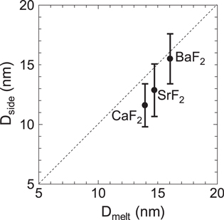
In the following, the relation between hillock diameter and that of the molten region is analyzed based on the conventional ATSM framework. Calculation of molten region diameter based on ATSM using the melting criterion is possible by using material parameters such as density, specific heat and melting temperature [48, 49]. The density is taken as 3.18, 4.24 and 4.89 g cm−3 for CaF2, SrF2 and BaF2, respectively. The specific heat is taken as 0.854, 0.543 and 0.410 J g−1 K for CaF2, SrF2 and BaF2, respectively. The melting temperature is shown above. Assuming the existence of the velocity effect, high efficiency (g = 0.4) is adopted here, since it is usually adopted for low velocity ions in the low velocity range of E < 2 MeV u−1. The calculated maximum molten region diameter (Dmelt) is compared with the hillock diameter (Dside) for fluorides as shown in figure 10. There is a clear correlation between Dmelt and Dside. Although hillock diameter is slightly larger than the molten region diameter for CaF2, the former shows similar behavior as the latter. The result shows that BaF2 is more susceptible to high electronic energy deposition than CaF2, and it is in accord with the trend found for the threshold potential energy necessary to form hillocks in CaF2 and BaF2 by highly charged ions (HCI) [55]. The present result for fluorides also demonstrates that hillock formation is closely related to transient melting due to the thermal spikes.
Figure 10. Relation between molten region diameter calculated by ATSM using the melting criterion (Dmelt) and hillock diameter at the side surface (Dside) for fluorides.
Download figure:
Standard image High-resolution image
5. Conclusions
Hillocks are successfully imaged by TEM for YIG and three fluorides (CaF2, SrF2 and BaF2) by irradiating with swift heavy ions at oblique incidence. We have demonstrated that hillock diameter and height can be accurately measured by using the present method. For YIG, the hillock diameter is comparable to ion track diameter, whereas for all the fluorides it is always larger than the ion track diameter. For YIG, which is a typical amorphizable material, hillocks are found to have amorphous structure which is in accord with the amorphous features of ion tracks. On the other hand, for non-amorphizable fluorides the hillocks are found to have crystalline features, and they are composed of nanocrystallites. The present results strongly suggest that hillock formation is closely related to melting along the ion path regardless of amorphizability of the materials. On the other hand, relatively small ion tracks for fluorides can be interpreted by assuming a recrystallization process within the framework of the thermal spike models. It is found that for fluorides both hillock and ion track diameters vary in the order of cation mass (i.e. CaF2 < SrF2 < BaF2). The trend found for the hillocks is consistent with the thermal spike model (for example, conventional ATSM adopted for amorphizable materials) assuming the existence of the velocity effect.
Acknowledgments
The authors are grateful to the technical staff of the accelerator facilities at JAEA-Tokai for supplying high-quality ion beams. The authors thank A Iwase, K Yasuda and H Amekura for fruitful discussions. Part of the present work was financially supported by JSPS KAKENHI Grant Number 16K06963.