


Abstract
Soil salinity index (SI) is a measure of salt concentration in soil water. The salinity index is calculated as a partial derivative of the soil bulk electrical conductivity (EC) with respect to the bulk dielectric permittivity (DP). The paper focused on the impact of different sensitivity zones for measured both EC and DP on the salinity index determination accuracy. For this purpose, a set of finite difference time domain (FDTD) simulations was prepared. The simulations were carried out on the model of a reflectometric probe consisting of three parallel rods inserted into a modelled material of simulated DP and EC. The combinations of stratified distributions of DP and EC were tested. An experimental verification of the simulation results on selected cases was performed. The results showed that the electromagnetic simulations can provide useful data to improve accuracy of the determination of soil SI.
Export citation and abstract BibTeX RIS
1. Introduction
Salt concentration in soil is a very important factor in environmental pollution monitoring [1, 2]. The most dangerous for the environment are soluble salts of heavy metals and an excessive amount of fertilizers [3, 4]. The development of soil salinity measurement methods can improve fertilization efficiency minimizing surface and ground water pollution. The electrical conductivity (EC) of saturated soil or soil water extracts [3–5] is the standard currently used to measure soil salinity. However, its measurement is time and labour-consuming and is impractical for monitoring purposes. An alternative method is measuring soil bulk EC. This method is easy to use and adaptable for monitoring system applications. Soil bulk EC determination is based on measurements of electromagnetic induction [6], electrical resistance, impedance and dielectric permittivity (DP) [7–11]. A disadvantage of this method is its susceptibility to soil moisture [12].
Salinity Index (SI) allows the determination of the salt concentration in soil water, regardless of the soil moisture level. SI is defined as a partial derivative of soil bulk EC with respect to the TDR-measured bulk DP [13] or the real part of complex relative DP [9], as shown in equation (1). In practice, taking advantage of the linear relation between soil bulk EC and DP at constant soil pore-water EC, SI can be calculated using a single measurement of ECb and DPb of a soil sample, according to the following formula

where ECi and DPi are the limiting values of EC and DP, respectively, for dry soil. After laboratory calibration of the model, EC of soil pore-water can be calculated as shown in [9, 13]. Originally, SI model was developed for the use with TDR the technique [13]. Recently, the performance of the SI model has also been evaluated using frequency-domain measurements [9, 14, 15].
Determination of SI requires simultaneous measurement of EC and DP. EC is calculated from the measured probe impedance at the low frequency range or from the pulse amplitude. Selective measurement of DP is possible only in the high frequency range, in order to avoid the impact of EC and electrode polarization on the measured value. Because of that, it is necessary to use broadband measurement methods.
Volumetric moisture distribution and the EC of soil samples under natural conditions are most often heterogeneous. This is caused by the occurrence of rainfall and continuous water evaporation from the soil surface as well as groundwater capillary rise. Gravity also contributes to the formation of a soil moisture gradient. Soil water evaporation causes a strong increase of salt concentration in the soil surface layer. Rainfall, on the other hand, causes the reverse process. Water supplied to the soil surface reduces the concentration of salts in the soil water. Due to the moisture gradient, salts contained within water are moved to lower soil layers.
The time domain reflectometry (TDR) [16] technique for the simultaneous determination of EC and DP from the needle pulse signal reflection should take into account the previously described gradients, which could occur inside the sensitivity area of the electrodes. The EC measurement is carried out in the volume of a material limited by its properties or, in the case of laboratory measurements, the sample container walls. We can say that it is the result of averaging in volume. DP is measured in a variable sensitivity zone of the TDR probe, which is dependent on the probe geometry, as well as moisture and dielectric dispersion properties of the examined material [17–19]. Therefore, simultaneous measurement of DP and EC takes place in two different zones of sensitivity.
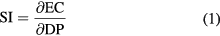
Heterogeneous distribution of moisture and EC in the volume of the material under test can cause errors in determining the SI. Figure 1 presents the impact of the measurement errors of EC and DP on SI calculated using equation (2), in the case when the surrounding material has lower EC and DP than the material under test. Once the errors of EC and DP as a function of the material-under-test thickness are known, the error of SI can be estimated from the maximum change of the calculated slopes. The aim of this study was to determine the effect of stratified distribution of the material dielectric properties parallel to the TDR probe rods on the SI. Parallel stratification of dielectric properties can occur in practice, e.g. if the probe is inserted in the wall of a soil profile, parallel to the soil surface. Electromagnetic simulations were carried out with the use of the EMPro software (Keysight) [20] for the TDR probe design with three parallel rods inserted into the material under test. The combinations of stratified distributions of the DP and EC were simulated. The results of numerical simulations consisted of the reflected voltage versus time response and the complex values of the reflection coefficient S11 in a broadband frequency range. We also determined the distribution of the electric field, in order to depict the shape and size of the sensitivity zone of the probe. An analysis of the error generated as a result of the limited sensitivity zone of the TDR probe was performed. An experiment was performed in order to verify the conclusions from the simulations. The results can be applied to improve the accuracy of the SI determination during evaporation and moistening processes in the soil.
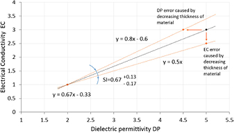
Figure 1. Impact of EC and DP measurement errors on the SI estimation.
Download figure:
Standard image High-resolution image2. Simulations
2.1. Probe model
The simulations were performed using a three-rod probe model design. The dimensions and design of the probe are shown in figure 2. The length and the distance between the rods were selected to minimize the volume of the material under test and also to minimize the amount of memory needed to perform the simulations. The probe design takes into account future manufacturing possibilities of the probe based on commercially available N-type connectors. The chosen design also enabled an experimental verification of the simulation results using a vector network analyser (VNA).
Figure 2. Simulated model of the TDR three-rod probe.
Download figure:
Standard image High-resolution imageThe FDTD excitation signal of the simulation model was applied by a 50 Ω coaxial port (EMPro add-on) which significantly improved the results. The simulations were conducted using a Fujitsu Celsius 930 workstation equipped with an NVIDIA Tesla K20 GPU.
2.2. FDTD mesh and material definition
Dielectric properties of artificial materials were defined by a single pole Debye model. We selected four non-conductive materials (EC = 0 mS m−1) with static DP εs = 10, 20, 40, 80, and three conductive materials with conductivity EC = 20, 100, 200 mS m−1 and fixed εs = 80. The remaining two Debye parameters: relaxation time, τ, and DP at the high frequency, ε∞, for all materials were fixed as 10 ps and 5, respectively, based on similarity to water properties.
During initial tests, the dimensions of the tested material and the density and structure of the FDTD mesh were optimized. We noted that the mesh changes between simulations had significant impact on the results. Parameters of the mesh were adjusted so that the mesh remained unchanged in subsequent iterations of the material thickness. The number of cells equalled to 106 × 56 × 166 with two density regions of vertical edge cell dimensions 0.2 mm and 1 mm (figure 3). The simulation box had total dimensions of 62 × 40 × 150 mm. The boundary condition of the simulation box was defined as the absorption 7 layer PML (perfect match layer) from all sides.
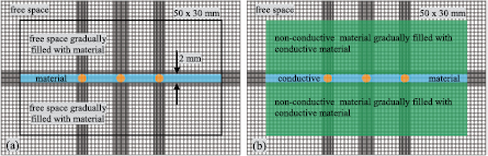
Figure 3. FDTD simulation mesh for 2 mm thickness of dielectric layer (a) and conductivity layer (b).
Download figure:
Standard image High-resolution image2.3. Methodology
The simulations focused on identifying sensitivity areas of the probe separately for measurements of bulk DP and EC. The excitation signal on the coaxial port was a Gaussian pulse of a 70 ps width. The obtained time domain results were analysed to extract the amplitude and time of the signal reflected from the end of the rods (figure 4). Additionally, probe impedance at 10 MHz was registered.

Figure 4. Time distances and amplitudes of TDR reflections from the end of the probe rods for different layer thicknesses of material with εs = 80 and EC = 0 mS m−1. Outside of the material there is free space (εs = 1).
Download figure:
Standard image High-resolution imageSimulations were performed sequentially for sixteen values of material thickness, which symmetrically surrounded the rods. The modelled material layer, placed parallel to the probe, was 20 mm longer than the probe rods, so that the reflection from the ends of the rods was not disturbed by the material termination. Material thickness was 2 mm, 2.8 mm and 4–30 mm every 2 mm. Simultaneously, the upper and lower part of the free space was diminished, respectively. The geometry and dimensions of the simulated material 2 mm thick, in cross-section perpendicular to the probe rods, were presented in figure 3. For seven materials, a total of 112 simulations were performed. To elucidate the relation between the measured TDR time and the thickness of the material layer, the distributions of the electric field around the probe rods were recorded. It enabled observing the shape and size of the sensitivity zone of the probe with the changes in material thickness. An assessment of the sensitivity area for the measurement of DP was made based on the simulation in non-conductive materials (figure 3(a)). In this case, the remaining part of an unfilled space was defined as free space, εs = 1. The sensitivity area of EC determination was studied by testing materials of different values of EC (figure 3(b)). In these cases, the rest of the space was filled with a material of EC equal to zero. This allowed to avoid the impact of the probe rods electrical capacitance on the measured impedance value of the probe. The square root of DP (refractive index) is an approximately linear function of TDR time. On the basis of changes in the value of the TDR time, we determined the relative error of DP in relation to the reference value of 30 mm material thickness layer. Similarly, the EC relative error was determined on the basis of changes of both the value of the probe impedance at 10 MHz and the TDR pulse amplitude.
3. Experimental verification
3.1. Measuring system
In order to verify the simulation results, an experiment was performed. The measuring system consisted of a Rohde and Schwarz VNA type ZVCE [21] (equipped with the option B2 Time Domain Measurements) and a three-rod probe placed in a container presented in figure 5.
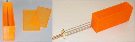
Figure 5. The probe and the experimental container for the simulation results verification.
Download figure:
Standard image High-resolution imageThe probe body was made of brass, in which the acid-resistant steel rods were embedded. The dimensions of the probe were identical to the simulation model shown in figure 2. The connection between the VNA and the probe was made using a semi-rigid cable RG401 and a soldered N-type connector. The container made from PLA (polylactic acid) plastics using a 3D printer was designed so that it allowed changing the thickness of the material, as described in the simulations, by using two additional internal removable, very thin (0.3 mm) walls. In this way, the vessel was divided into an inner chamber of a variable width, containing the TDR probe and, symmetrically, two outer chambers.
3.2. Experimental technique
The VNA performed 800 measurements of the S11 parameter in the frequency range from 10 MHz to 8 GHz. The measurements were preceded by a single-port OSL calibration using the N-type ROSENBERGER calibrators. The Time Domain Measurements option of the VNA was used to determine the time and amplitude of the needle pulse signal reflected from the end of the probe rods whilst the module of impedance at 10 MHz was obtained directly. Trying to comply with the simulation methodology given in section 2.3, the verification measurements were performed using in the first case distilled water and air, and in the second case distilled water and KCl water solutions in three levels of EC = 20, 100, 200, mS m−1. Water was poured between walls, accordingly to the simulations conditions.
4. Results and discussion
Figures 6 and 7 show six cross-sections of electric field magnitude distributions at half length of the probe rods. The evaluation of the DP sensitivity zone shape was conducted at 1 GHz (figure 6), whilst for EC the frequency of 10 MHz was used (figure 5). It was evident that increasing the material thickness decreased the magnitude of electric field located outside of the material. However, it was very difficult to determine the exact value of the TDR time readout error from the comparison between the cases. We could only notice that some electric field appeared on both sides of the material for thickness lower than 12 mm. It meant that insufficient signal attenuation in the material caused additional readout errors.
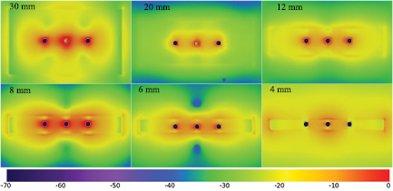
Figure 6. Electric field magnitude (dB) at 1 GHz for different thicknesses of the material layer with εs = 80 and EC = 0 m Sm−1. Outside of the material there is free space, εs = 1.
Download figure:
Standard image High-resolution image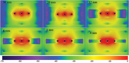
Figure 7. Electric field magnitude (dB) at 10 MHz for the material with εs = 80 and electrical conductivity of the layer equal to 200 mS m−1 and outside the layer to 0 mS m−1.
Download figure:
Standard image High-resolution imageIn figure 7, the 200 mS m−1 conductivity layer behaves like an absorber for low frequency electric field. As in the previous case of DP, it is very difficult to designate the exact value of the EC readout error. It is worth to notice that decreasing the conductive layer thickness increased the electric field magnitude between the rods. The opposite behaviour was observed for the results depicted in figure 6.
Based on the conducted simulations, absolute values of the relative error for different DP and EC were calculated. The reference values for the calculations were taken from the results obtained for 30 mm material thickness. The relative error was therefore determined as a ratio of the value obtained for a given material thickness x and the reference value for 30 mm: ERRrel = |t30 − tx|/t30, or for the pulse amplitude: ERRrel = |A30 − Ax|/A30. The relation between the relative error and material thickness is very useful in evaluating sensitivity areas for certain error levels. The SI calculation requires measuring DP and EC simultaneously. Because the EC and DP error values versus thickness of material were different, one should consider the selection of the worst case for the determination of the calculated SI error. Figure 8 shows the comparison of relative errors versus thickness of the material. Error level below 1% was achievable for material thickness bigger than 20 mm.
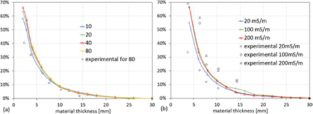
Figure 8. Comparison of relative errors for two types of measurement, (a) DP from TDR time, (b) EC from impedance at 10 MHz. Black points represent the experimental results.
Download figure:
Standard image High-resolution imageThe results of the experimental verification performed on distilled water and the KCl solutions of electrical conductivities consistent with the simulations parameters were included in figure 8. As can be seen in figure 8(a), the relative errors for DP obtained from the experiment were close to the simulation results and exhibited the same trend. The experimental values were slightly lower than the values obtained from the simulations. It is to be noted, however, that the simulation setup did not include 0.3 mm thick inner walls separating water and air in the experimental container. Additionally, the walls were subjected to deformation due to the water pressure.
The errors obtained experimentally for EC also exhibited similar trends as in simulations, as can be seen in figure 8(b). However, the experimental values differed more from the simulation results than in the case of DP. It was so because the EC determination was much more sensitive to the presence of the inner separating, electrically insulating walls than in the case of DP measurements.
Also, we can notice that the method of EC determination was very important with regard to the SI calculation. Figure 9 presents the EC measurement error calculated on the basis of the amplitude of the TDR pulse. The experimental results exhibited the same trends as in simulations. The differences between the experimental and simulation values were caused by the presence of the inner separating, electrically insulating container walls, as in the case of EC calculated from impedance (figure 8(b)). In contrast to the impedance method (figure 8(b)), the relative error increased with EC. In the case of 1% error for the 20 mm sensitivity area, the selected method had no significance. For lower material thickness, it should be better to use impedance EC determination method.

Figure 9. Relative errors of EC calculated from the TDR pulse amplitude. Black points represent experimental results.
Download figure:
Standard image High-resolution image
5. Conclusions
The DP and EC relative errors calculated from TDR time and impedance at 10 MHz, respectively, depended on the thickness of the material. The experimental results confirmed the trends obtained from the simulations. The exact error values increased and differed between DP and EC when material thickness decreased below 20 mm. At thickness higher than 20 mm, the error of both DP and EC was below 1%. It turned out that the safe sensitivity area for the determination of SI was about 20 mm for the geometry of the simulated probe. Below 20 mm of material thickness, the EC calculated from TDR needle pulse amplitude was strongly dependent on the absolute value of EC. In this case, this method should not be used for SI calculation.
Acknowledgment
The presented work was supported by the National Science Centre, Poland, in the scope of the research project no. 2014/15/D/ST10/04000.