

Abstract
At present, chips urgently need breakthrough development in the power consumption and integration. The chip integrates billions or even tens of billions of electronic components, such as field effect transistor, diode and so on. Therefore, the research and development of new low-power electronic components with smaller size is an effective method to reduce chip power consumption and improve chip integration. In this paper, the ferroelectric field effect transistor (Fe-FET) based on two-dimensional heterostructures α-In2Se3/ZnSe is proposed. Based on the first principle, the program will analyze the stability and band structure of α-In2Se3/ZnSe under different stacking modes. In the heterojunction, the microphysical mechanism of ferroelectric polarization affecting the electronic structure is revealed from the aspects of charge transfer at the interface and the asymmetric surfaces with different work function. Combined with the non-equilibrium Green's function transport theory, the transport properties of Fe-FET based on their α-In2Se3/ZnSe will be studied. The application will provide sufficient theoretical support for research and development of the device based on α-In2Se3/ZnSe structure.
Export citation and abstract BibTeX RIS
1. Introduction
The development of chip technology faces two main problems—how to reduce the power consumption of chips and improve the integration of chips. At present, the exploration and development of new low-power electronic components with smaller size, including FETs, diode and so on, is regarded as an effective method to solve these problems. In the exploration of reducing the power consumption of chips, the research of ferroelectric field effect transistors (Fe-FETs) is gradually rising [1, 2]. Ren et al has developed an all inorganic flexible Fe-FET with low power consumption, high switching ratio and good retention based on the Pb(Zr0.1Ti0.9)O3/ZnO heterojunctions [1]. Under repeated bending and high temperature conditions, the FETs can still maintain good electrical properties. Chai et al realized firstly the function of non-volatile Fe-FETs on LiNbO3 ferroelectric film [2]. Compared with traditional FETs, the gate dielectric layer is replaced by ferroelectric thin film (FTF) in Fe-FETs. The Fe-FETs induce the polarization reversal of FTFs only by applying a transient bias voltage. The polarization state of FTF further control 'off' and 'on' of Fe-FETs by modulating the semiconductor surface state. The principle is shown in figure 1(a). The traditional FETs needs to continuously apply voltage to convert 'off' and 'on', as shown in figure 1(b). Therefore, the Fe-FET is more energy-saving and low consumption than FET. However, FTFs based on traditional Perovskite materials have obvious disadvantages. When the thickness of Perovskite ferroelectric film is lower than a critical size, the ferroelectric polarization will disappear. The size effect will restrict the integration of the device [3–6].
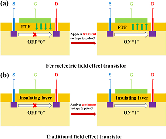
Figure 1. (a) The schematic diagram of Fe-field effect transistor (FET). (b) The schematic diagram of FET. FTF is the abbreviation of ferroelectric thin film.
Download figure:
Standard image High-resolution imageHow to reduce the size of nano-electronic components and improve the integration of chips? The emergence of two-dimensional (2D) materials makes it possible to solve this problem. Since Geim and Novoselov successfully obtained stable graphene by mechanical stripping in 2004, 2D materials have rapidly become hotspots in the fields of condensed matter physics, chemistry, material science and electronics [7, 8]. In addition to graphene, 2D materials also include transition metal disulfide, silicon carbide, black phosphorus and so on [9–12]. They exhibit rich and excellent electrical, optical and mechanical properties. Moreover, the heterostructure composed by different 2D materials bring new ideas for the design of small-size nano-electronic components with high performance and special functions [13–16]. Thus, the Fe-FETs based on 2D heterostructures inherit the characteristics of low power consumption and small size. However, from 2004 to 2015, 2D materials with out-of-plane ferroelectricity was not found. The research of Fe-FETs based on 2D heterostructures has not made progress. Until 2016, Belianinov et al and Liu et al observed firstly the 2D material CuInP2S6 with the out-of-plane ferroelectricity [17, 18]. In 2017, Ding et al calculated and predicted α-In2Se3 has in-plane and out-of-plane ferroelectricity by using first principles. The process of ferroelectric polarization reversal is described and the barrier height is calculated [19]. In 2019, Si et al firstly developed the Fe-FETs based on α-In2Se3 [20]. Because the research of device based on α-In2Se3 is still in its infancy, many related problems have not been solved, including mainly the microphysical mechanism of ferroelectric polarization α-In2Se3 controlling the band structure of heterostructures and so on.
In this paper, we calculated the effect of ferroelectric polarization on the electronic properties of the heterostructure α-In2Se3/ZnSe by employing the density functional theory (DFT) based on the first-principles methods. The polarization reversal barrier of ferroelectric heterostructures is calculated by nudged elastic band (NEB) method. The calculation of electronic properties shows that the α-In2Se3/ZnSe heterostructure changes from metal to semiconductor by ferroelectric polarization reversal. The physical mechanism of ferroelectric polarization changing the electronic structure is described. Finally, the transport properties of devices based on α-In2Se3/ZnSe are also discussed. This work provides a valuable reference for designing electronic components.
2. Computational methods
DFT calculations were carried out using the Vienna ab-initio Simulation Package [21, 22]. The generalized gradient approximation (GGA) of the Perdew–Burke–Ernzerh (PBE) exchange-correlation functional is employed in all calculations. However, as is well known, the band gap will be underestimated when the GGA–PBE method is used. Thus, the Heyd−Scuseria−Ernzerhof hybrid functional (HSE06) was used to correct the band gap calculations [23]. The calculations are performed using 7 × 7 × 1 Monkhorst–Pack k-point meshes. The energy cutoff is set at 400 eV. The structure relaxation was stopped until the force on each atom is <0.01 eV Å−1. To avoid interaction due to two neighboring images, the vacuum space is >15 Å[24]. Dipole correction is also considered to eliminate electrostatic potential errors. The DFT-D3 method was also employed to describe the van der Waals interactions[25]. For the NEB calculation, the 4 × 4 × 1 super cell and 7 × 7 × 1 Monkhorst–Pack k-point meshes are used. For the calculation of transmission spectrum of device, the first-principles software package Atomistix Toolkit (ATK) from Quantum Wise based on the DFT combined with nonequilibrium Greens functions is employed. The GGA is used for exchange-correlation potential. The cutoff energy of 150 Ry and a Monkhorst–Pack K-mesh of (1, 1, 100) are used. The single-zeta polarized basis set is adopted for electron wave function. All atomic positions are fully relaxed using quasi-Newton method until the force tolerance to 0.02 eV Å−1 [26, 27].
3. Results and discussion
Figure 2(a) shows the atomic structures of ZnSe and α-In2Se3 respectively. The optimal lattice parameter is 4.09 Å for ZnSe, which exhibits a honeycomb structure like graphene with high symmetry. The optimized lattice constant of ZnSe is also close to the previous studies[28]. The optimal lattice parameter is 4.10 Å for α-In2Se3, which is consistent with other experimental and theoretical works, 4.09 Å [19]. The lattice constants of ZnSe and α-In2Se3 are very similar. Thus, the cells of 1 × 1 × 1 and 1 × 1 × 1 are used for ZnSe and α-In2Se3, respectively. And the lattice mismatch between the ZnSe/α-In2Se3 heterostructure interface is small, only 0.24%. It is almost unnecessary to consider the effect of excessive contact interface strain on stability of heterostructures and their electronic structures. Figures 2(b) and (c) show the electronic structures of ZnSe and α-In2Se3 calculated by the HSE06 hybrid functional. The single α-In2Se3 layer is a semiconductor with an indirect band gap, about 1.50 eV. And the single ZnSe layer have a direct band gap, 3.0 eV. Figures 2(d) and (e) are the electrostatic potential distribution along the c direction of α-In2Se3 and ZnSe respectively. The ferroelectricity of α-In2Se3 induces the different potential ΔV of the two surfaces [29, 30].
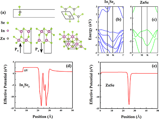
Figure 2. (a) Atomic structure of α-In2Se3 and ZnSe. (b), (c) Band structure of α-In2Se3 and ZnSe. (d), (e) Electrostatic potential of α-In2Se3 and ZnSe.
Download figure:
Standard image High-resolution imageThen four α-In2Se3/ZnSe heterostructures are considered, including two stacking way (stacking I and stacking II), as shown in the figures 3(a), (c), (f) and (h). As for the ferroelectric heterostructures, the top and side views of ZnSe/α-In2Se3 have two opposite polarization states. With the reversal of ferroelectric polarization (P↑ , P↓ ), the structure in the figure 3(a) (structure I with P↓ ) will be transformed into the structure in the figure 3(f) (structure I with P↑ ), and the structure in the figure 3(c) (structure II with P↓ ) will be transformed into the structure in the figure 3(h) (structure II with P↑ ). The figure 3(b), (d), (e) and (g) show the transition paths of the four heterostructures and the potential barriers to be overcome. The transformation of structures with different stacking modes requires needs to overcome the large barrier, 0.191 eV per−1 cell and 0.788 eV per−1 cell as shown in the figures 3(b) and (g). Certainly, the barrier prevents the transformation between structures, which ensures the relative stability of different heterostructures. But the barriers of ferroelectric polarization reversal are small, 0.037 eV per−1 cell and 0.074 eV per−1 cell respectively as shown in the figures 3(d) and (e).
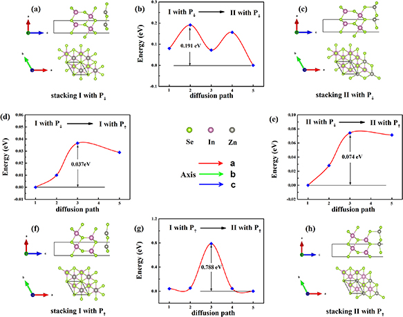
Figure 3. (a), (c), (f) and (h) the atomic structure of four α-In2Se3/ZnSe heterostructures. (b), (d), (e) and (g) The transition paths of the four heterostructures and the potential barriers/per cell. The 4th points are omitted in the (d) and (e).
Download figure:
Standard image High-resolution imageThe 4th points are omitted in the figures 3(d) and (e) are omitted. We explain as follows: It is worth noting that there are transition states (the 4th points) with energy lower than final states (heterostructures with P↑ ) in the figures 3(d) and (e). The atomic structures of transition states and heterostructures with P↑ were compared in the figure 4. The structures of transition states are very similar to heterostructures with P↑ . The difference is that the In-Se bonds (shown by the red circle in the figure 4) are not parallel to the lattice c direction in the transition state structures. The energy difference between the transition states and the final states are less than 0.01 eV per−1 cell. When optimizing the structure, both the changes of lattice and atomic position will be considered. The lattice of the heterostructures with P↑ are 4.06 Å and heterostructures with P↓ are 4.10 Å. For NEB calculation, the lattices of the initial state (with P↓ ) and the final state (with P↑ ) are fixed at 4.10 Å in this paper. The lattice change was ignored in NEB calculation, resulting in the transition state with lower energy. Considering the lattice change, the structure of the transition states was optimized into the heterostructures with P↑ according to our calculations. The relevant data about NEB calculation and optimization calculation are shown in the table 1. According to the above analysis, the final states are more stable than the transition states (the 4th points).
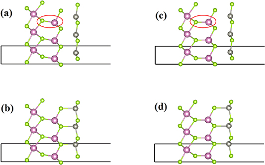
Figure 4. (a) and (b) The atomic structures of transition states as shown in the figures 3(d), (e). (c) and (d) the atomic structures shown in the figures 3(f), (h).
Download figure:
Standard image High-resolution imageTable 1. The lattice and energy in the NEB calculation and optimization calculation.
| NEB calculation | Optimization calculation | |||
|---|---|---|---|---|
| Lattice (Å) | Energy (eV) | Lattice (Å) | Energy (eV) | |
| The 4th state (in figure 3(d)) | 4.096 | −24.97 | Same as the final state | |
| The final state (in figure 3(d)) | 4.096 | −24.96 | 4.057 | −24.98 |
| The 4th state (in figure 3(e)) | 4.096 | −25.01 | Same as the final state | |
| The final state (in figure 3(e)) | 4.096 | −25.00 | 4.063 | −25.02 |
The barrier of polarization reversal is an important physical parameter for Fe-FETs. If the barrier of polarization reversal is too large, the Fe-FETs need a great external voltage to work. The asymmetry of diffusion path is caused by the asymmetry of heterostructure in the vertical direction. Ding et al concluded that the potential barrier of ferroelectric polarization reversal of monolayer α-In2Se3 was 0.066 eV per−1 cell [19]. Therefore, the heterostructures does not cause obvious changes in the polarization reversal barrier of α-In2Se3. According to the study of Ding et al, the ferroelectric polarization of heterostructures can be regulated by normal range external electric field about 0.3 V Å−1.
According to the distribution of differential charge, we further analyze the structural characteristics of heterostructures as shown in the figures 4(a)–(d). The differential charge is calculated by formula:
where the  ,
,  and
and  are the charge densities in the heterostructure, α-In2Se3 and ZnSe at the (x, y, z) point, respectively. For the heterostructures with stacking I, the efficient electrons accumulate at the Se atoms of α-In2Se3, while the efficient holes accumulate at the Zn atoms of ZnSe as shown in the figures 5(a) and (b). The minimum distances between the Se atoms of α-In2Se3 and the Zn atoms of ZnSe are 3.71 Å and 3.82 Å in the figures 5(a) and (b), which are greater than the sum of the ion radii of Zn and Se, 2.72 Å (Zn ion radii is 0.74 Å and Se ion radii is 1.98 Å). Thus, there is no bond between α-In2Se3 and ZnSe. The heterostructures with stacking I show the structural characteristics of van der Waals heterostructure. As shown in the figure 5(c), the efficient holes accumulate at the Zn atoms of ZnSe and the Se atoms of α-In2Se3, while the efficient electrons accumulate at middle region of Zn and Se atoms. And the minimum distances between the Se atoms of α-In2Se3 and the Zn atoms of ZnSe is 2.72 Å, which equals the sum of the ion radii of Zn and Se. These suggest that new chemical bonds formed between ZnSe and α-In2Se3. As shown in the figure 5(d), the distribution of differential charge is similar to that in the figure 5(c). However, comparing the ordinates of figures 5(c) and (d), the latter accumulates less charge in the middle region of the heterostructure. The minimum distances between the Se atom of α-In2Se3 and the Zn atom of ZnSe is 2.93 Å > 2.72 Å. These imply that no chemical bond formed between ZnSe and α-In2Se3 in the figure 5(d). The heterostructure in the figure 5(d) also show the structural characteristics of van der Waals heterostructure.

Figure 5. The differential charge of the α-In2Se3/ZnSe heterostructures with different stacking modes and ferroelectric polarization. The yellow and blue areas denote electron accumulation and hole accumulation, respectively.
Download figure:
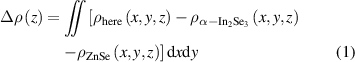
Standard image High-resolution imageThe structural differences of heterojunctions may lead to obvious differences in electronic structures. Thus, the electronic structure of α-In2Se3/ZnSe heterostructures are studied and discussed. The electronic structures shown in the figures 6(a)–(d) are calculated by GGA–PBE. However, the band gaps calculated by GGA–PBE are lower than the actual gaps. To correct the band gaps, the electronic structures are calculated by HSE06 function as shown in the figures 6(e)–(h) [31]. The electronic structures calculated by the two function are consistent in the shape and trend of bands except for the different gaps. (In the following discussion, the band gaps of heterostructures are calculated by HSE06 functional.)
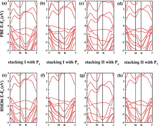
Figure 6. (a)–(d) Bands calculated by GGA. (e)–(h) Bands calculated by HSE06. Green and blue lines represent the valence band with the highest energy and the conduction band with the lowest energy, respectively.
Download figure:
Standard image High-resolution imageFor the α-In2Se3/ZnSe heterostructure with stacking I, the heterostructure is a semiconductor with direct band gap about 0.76 eV in the case of P↓
as shown in the figures 6(a) and (e). In the case of P↑
, the heterostructure is still a semiconductor, but it shows indirect band gap with 1.56 eV as shown in the figures 6(b) and (f). Polarization reversal causes great changes in the valence band morphology and band gap. For the α-In2Se3/ZnSe heterostructure with stacking II, the band gap is zero. The conduction band and valence band are closed at point  . Thus, the heterostructure exhibits metallic properties as shown in the figures 6(c) and (g). With the ferroelectric polarization reversal, the heterostructure changes from metal to semiconductor with direct band gap about 1.3 eV. Except for the band gap, the morphology of the band structure has not changed significantly.
In order to analyze the distribution of electronic states, the projected density of states distribution of heterostructures is explored by GGA–PBE as shown in the figures 7(a)–(d). The DOS distribution can also underestimate the band gap of heterostructures, but can reflect the composition of electronic states. For the α-In2Se3/ZnSe heterostructure with stacking I (P↓ ), the states are contributed by ZnSe near the valence band maximum (VBM) and by α-In2Se3 near the conduction band minimum (CBM). Thus, the heterostructure with stacking I (P↓ ) shows type-II band arrangement. The α-In2Se3/ZnSe heterostructure with stacking I (P↑ ) shows type-I band arrangement, because the states are both contributed by α-In2Se3 near the VBM and CBM. We also projected the occupied states of α-In2Se3 and ZnSe into the bands as shown in the figures 8(a)–(d). The contribution of α-In2Se3 and ZnSe in the bands is more intuitively displayed. Polarization reversal changes the DOS distribution of the valence band, resulting in the morphological change of the valence band top, as discussed above. By controlling the polarization direction of FTFs, the interfacial charge transfer behavior of heterostructures is changed. The type-I heterojunction shows the enhancement of α-In2Se3 luminescence, while type-II heterojunction shows the quenching of α-In2Se3 luminescence. The transition of band arrangement and the regulation of interlayer charge transfer behavior are of great value to the research of 2D semiconductor materials in optoelectronic properties and the application of integrated information devices.

Figure 7. The projected density of states (PDOS) distribution of α-In2Se3/ZnSe heterostructures with different stacking modes.
Download figure:
Standard image High-resolution image
Figure 8. The band structures and orbital spatial distributions of α-In2Se3/ZnSe heterostructures.
Download figure:
Standard image High-resolution imageAs mentioned earlier, this phenomenon of energy level change is attributed to the ΔV in the figure 2(d). With the P↓ changing to P↑ , the ΔV causes the band of α-In2Se3 (as shown by the yellow and green lines) to shift upward relative to the Fermi level of heterostructure, while the band of ZnSe (as shown by the red and blue lines) shifts downward relative to the Fermi level. Comparing the figures 7(c) and (d), the same phenomenon can also be observed. As shown in the figure 7(c), the band of ZnSe pass through the Fermi level. Near the Fermi level, there are a large number of Se electronic states (from ZnSe and α-In2Se3) and a small number of In electronic states from α-In2Se3. The result also implies there is a weak bond between Se atoms of ZnSe and In atoms of α-In2Se3. And the newly formed bond in the heterostructure with stacking II and P↓ is an important reason for the metallicity. After the band of ZnSe shifts downward, the metallic properties of heterostructure disappears as shown in the figure 7(d). The phenomena that the ferroelectric polarization controls the metallicity and semi-conductivity of heterostructure are widely used in Fe-FETs.
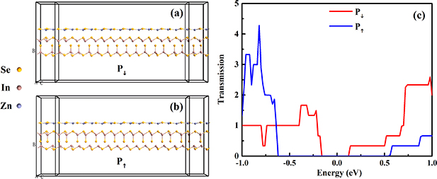
Finally, we discussed the transmission spectrum of ferroelectric tunnel junction (FTJ) based on the heterostructures with stacking II. As shown in the figures 9(a) and (b), the α-In2Se3/ZnSe FTJs are composed of three parts: left lead (L), right lead (R), and the central scattering region (C). In the figure 9(c), the transmission spectrum of FTJs with different ferroelectric polarization are compared. Although the heterostructure with P↓ shows metallicity, the FTJ based on the heterostructure with P↓ still shows a small gap in the transmission spectrum, from −0.16 eV to 0.12 eV. Because the crystal structures of heterostructure is used to calculate the band structure. But the calculation of transmission spectrum is based on nanoribbons, whose periodicity is lower than that of crystal structure. The strong edge effect of nanoribbons opens the band gap of heterojunction. In other reports, this phenomenon also were observed. For example, the crystal structure of graphene has no band gap, while the armchair graphene nanoribbon is semiconductor. The transmission spectrum of FTJ based on the heterostructure with P↑ show larger gap than that of heterostructure with P↓ , from −0.62 eV to 0.54 eV.
Figure 9. (a)–(c) The transmission function for both polarization directions, with the Fermi level set to 0 eV.
Download figure:
Standard image High-resolution image
According to formula (2), the transmission spectrum coefficient also determines the transmission current. The tunnel current Is is obtained by the formula [32, 33]:
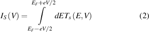
where Ts is the transmission coefficient of the FTJ, EF is the Fermi level, and V is the bais voltage between the source and drain of the device. And e and ħ are electron charge and Planck constant, respectively. We also compare our data with some related works. For example, Kang et al [34] calculated the transmission spectrum of FTJ based on graphene/α-In2Se3, in which the transmission coefficient is much smaller than that introduced in our paper [34]. This implies that the transmission current of device based on heterostructure α-In2Se3/ZnSe is obvious and considerable.
4. Conclusion
Based on the first principle, heterostructures α-In2Se3/ZnSe with different stacking modes and ferroelectric polarization are carefully analyzed and studied in this paper. According to the NEB calculation, the large potential barrier is the guarantee for the relative stability of the heterostructures with different stacking modes. And the barriers to overcome the polarization reversal of α-In2Se3 are 0.037 eV per−1 and 0.074 eV per−1, which are similar to the potential barrier of monolayer α-In2Se3, 0.066 eV per−1. This indicates that the asymmetry of heterostructure will not affect the polarization reversal of α-In2Se3. For the heterostructures with stacking I, the interfacial charge transfer behavior of heterostructures is changed by controlling the polarization direction of FTFs. For the heterostructures with stacking II, the electronic structure calculation shows that ferroelectric polarization can controls the metallicity and semi-conductivity. The possibility of polarization control device current is proved theoretically. The calculation of transmission spectrum implies that the transmission current of device based on heterostructure with staking II is obvious and considerable. This work provides a valuable reference for studying electronic characteristics of α-In2Se3/ZnSe and designing the low dimensional Fe-FETs.
Acknowledgments
The work was supported by Scientific Research Fund of Hunan Provincial Education Department (Grant Nos. 21B0405 and 21B0593). We also acknowledge Hunan Provincial Natural Science Foundation of China (Grant Nos. 2018JJ2148, 2020JJ5207 and 2021JJ40227) and National Natural Science Foundation of China (No. 12204166).
Data availability statement
All data that support the findings of this study are included within the article (and any supplementary files).
Conflict of interest
There are no conflicts of interest to declare.