

Abstract
The bandgap behavior of 2D-GaAs and graphene have been investigated with van der Waals heterostructured into a yet unexplored graphene/GaAs bilayer, under both uniaxial stress along c axis and different planar strain distributions. The 2D-GaAs bandgap nature changes from  -K indirect in isolated monolayer to
  -
- direct in graphene/GaAs bilayer. In the latter, graphene exhibits a bandgap of 5 meV. The uniaxial stress strongly affects the graphene electronic bandgap, while symmetric in-plane strain does not open the bandgap in graphene. Nevertheless, it induces remarkable changes on the GaAs bandgap-width around the Fermi level. However, when applying asymmetric in-plane strain to graphene/GaAs, the graphene sublattice symmetry is broken, and the graphene bandgap is open at the Fermi level to a maximum width of 814 meV. This value is much higher than that reported for just graphene under asymmetric strain. The
  -
- direct bandgap of GaAs remains unchanged in graphene/GaAs under different types of applied strain. The analyses of phonon dispersion and the elastic constants yield the dynamical and mechanical stability of the graphene/GaAs system, respectively. The calculated mechanical properties for bilayer heterostructure are better than those of their constituent monolayers. This finding, together with the tunable graphene bandgap not only by the strength but also by the direction of the strain, enhance the potential for strain engineering of ultrathin group-III-V electronic devices hybridized by graphene.
Export citation and abstract BibTeX RIS
1. Introduction
The unique physical properties of two-dimensional graphene- related materials, such as low dimensionality, enhanced flexibility, high mechanical strength, lightness, in-plane covalent bonding and dangling-bond-free lattice, allow them a variety of potential applications e.g. catalysis, biomedicine, conductive inks, sensors, coatings, light-emitting devices, composites, storage and production of energy, touch panels and high frequency electronics, among others [1–8]. Therefore, during the last ten years, the scientific community has developed an intense research on 2D nanomaterials, e.g. graphene [9], X-enes (X = B, Si, Ge, Sn, P, Bi) [10–18], X-anes (graphane, silicane, germanane, stanane) [19, 20], fluro-X-enes [20], MXenes [21], IIIV systems [22–27], transition metal dichalcogenides [28–31], layered oxides [32], layered double hydroxides (LDHs) [33], metal-organic frameworks [34, 35], covalent organic frameworks [36], polymers [37–39] and metals [40–43].
Recently, theoretical and experimental research has focused on the study of van der Waals (vdW) heterostructures by controlled multi-stacking of diverse layering materials such as metals, semiconductors or insulators [1, 44–46]. These hybrid materials will display interesting structural, electronic, optical and mechanical properties different from those of the 2D materials they are built of. Hence, they can be used to design new electronic and optoelectronic devices with unprecedented features or unique functionalities, such as tunnelling transistors, barristors, flexible electronics, photodetectors, photovoltaics and light-emitting devices [46]. Due to the special physical properties of graphene, e.g. its electrons display ballistic charge transport, graphene is to date the most common component in the van der Waals electronic devices [47]. Unfortunately, graphene lacks a bandgap, which is essential for controlling the conductivity by electronic means [48].
The absence of a gap in graphene, together with the linear dispersion of the bands at K point and the equivalence of the two carbon sublattices, restrains the Dirac fermions from getting a finite mass, which constrains the use of graphene in electronic devices. The importance of inducing a bandgap in graphene relies on generating an effective mass for the Dirac fermions, which offers the potential to improve the characteristics of graphene-based field-effect transistors [49]. This bandgap drawback has motivated researchers to employ 2D-materials beyond graphene. It has been found in these studies that graphene bandgap can be modulated by adsorption of H and F [20, 48], and in graphene-based heterostructures [44, 45, 50, 51]. The electronic structure of a heterostructure can also be tuned by applying strain [52].
Graphene-group III-V heterostructures have been studied in bilayer [49] and multilayer systems [53, 54] in order to tune the graphene band gap for optoelectronic applications. Giovannetti et al [49] studied graphene on single layer h-BN by density functional calculations. They found that the presence of h-BN breaks the sublattice symmetry of graphene, inducing a bandgap of 53 meV. Direct growth of graphene on h-BN and vice versa has been achieved by CVD methods [5, 55, 56]. Using first principle calculations, Kaloni et al [53] predicted finite and tunable bandgaps for superlattices in which a single graphene layer alternates with h-BN slabs of variable thickness. In addition, heterostructures where one, two or more graphene (other 2D-materials) layers sandwiched between two other 2D-materials (graphene) have been studied [54, 57, 58].
Therefore, in this work we consider the electronic structure and mechanical properties of a graphene-2D GaAs bilayer. We study first the structural properties and dynamical stability of graphene/GaAs bilayer, then its electronic and mechanical properties and, finally, the effect of both uniaxial stress along c axis and different planar strain distributions on the electronic properties. This study has been carried out using vdW–Tkatchenko–Scheffler (vdW-TS) method [67] and including spin–orbit coupling (SOC) within the DFT framework [68, 69].
The following scientific findings motivated us to carry out the present study:
- (i)
- (ii)
- (iii)
- (iv)
- (v)To the best of our knowledge, there are no previous studies about tuning the bandgap in graphene/GaAs bilayer heterostructures.
2. Computational and theoretical details
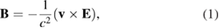
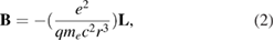
The calculations were performed using Vienna ab initio simulation package (VASP) [70, 71] employing the first principles pseudo-potential method in the framework of the DFT [68, 69]. The vdW-TS method [67] and the SOC have also been taken into account in our calculations. Exchange and correlation effects were treated with generalized gradient approximation implemented in the Perdew–Burke–Ernzerhof functional [72]. The core electrons were described by the projector augmented wave (PAW) method [73, 74] wherein the d states for Ga and As were included as valence electrons in their PAW pseudo-potentials. The valence electron configurations for C, Ga and As are considered as 2s22p 2, 3d104s24p 1 and 3d104s24p 3, respectively. The hexagonal primitive cell, with one Ga atom and one As atom, see figure 1(b), was constructed from the zinc-blende structure in the (1 1 1) plane [24]. In order to reduce the mismatch between graphene and 2D-GaAs hexagonal monolayers in graphene/2D-GaAs bilayer, a 551/331 supercell geometry has been used in this study, as shown in figures 1(a)–(c), respectively. The electron wave function was expanded in plane waves up to a cutoff energy of 500 eV for all the calculations. A Γ-centered grid of 25  25
25  1 k-points has been used to sample the irreducible Brillouin zone in the Monkhorst–Pack special scheme [75] for calculations, except for the supercell of the bilayer heterostructure where a 8
  8
8  1 k-point grid was used. Phonon calculations have been performed by taking into account the interactions in a 10
  10
10  1-graphene/6
  6
6  1-GaAs supercell [76]. The PYPROCAR code was used to plot the electronic bands of graphene/GaAs bilayer [77]. In addition, a 20
  vacuum spacing between the adjacent supercells is kept to avoid interactions. The optimized parameters for graphene, 2D-GaAs monolayers, and the 551-graphene/331-GaAs bilayer are given in table 1. Stress-based approach is implemented [78, 79] to study the mechanical properties, where the elastic tensor is determined by performing finite distortions of the optimized lattice and deriving the elastic constants from the strain-stress relationship (Hooke's law) [78, 79].
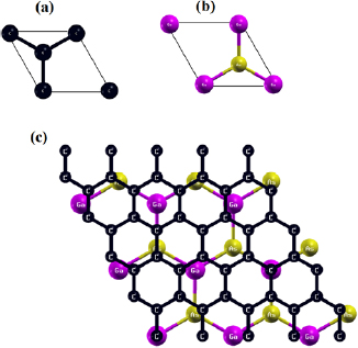
Figure 1. Honeycomb unit cells for (a) graphene, (b) 2D-GaAs monolayer, and (c) 551-graphene/331-GaAs bilayer heterostructure.
Download figure:
Standard image High-resolution imageTable 1. Calculated lattice constant (a ( )), angle between neighboring bonds (
 ), planar (PL) or low-buckled (LB) geometry, buckling parameter (
 (
( )), nearest-neighbor distance (d), interlayer distance (dL), and bandgap value (EG) for 2D graphene and GaAs monolayers, and graphene and GaAs within the 551-graphene/331-GaAs bilayer.
a ( ) ) |
 |
G |  ( ( ) ) |
d ( ) ) |
dL ( ) ) |
EG (eV) | |
|---|---|---|---|---|---|---|---|
| Graphene | 2.465 | 120 | PL | 0 | 1.423 | — | 0 |
| 2.460 [25] | 120 [25] | PL [25] | 0 [25] | 1.420 [25] | — | 0 [25] | |
| 2D-GaAs | 4.048 | 114.4 | LB | 0.577 | 2.407 | — | 1.03  |
| 4.050 [24] | 114.3 [24] | LB [24] | 0.550 [24] | 2.410 [24] | 1.08  [24] [24] |
||
| 3.970 [25] | 114.7 [25] | LB [25] | 0.550 [25] | 2.380 [25] | 1.29  [25] [25] |
||
| 551-graphene/ 331-GaAs | |||||||
| Graphene | 2.459 | 120 | PL | 0.001 | 1.419 | 3.476 | 0.005 KK |
| GaAs | 4.091 | 115.8 | LB | 0.501 | 2.427 | — | 0.720  |
In our study, the spin–orbit interaction has been taken into account. Spin–orbit coupling is a relativistic interaction between moving electrons with  and a local electric field
 in their rest frame created by the proton, where q is the charge of the moving electrons and
  is the electrostatic energy of the electron. Special relativity indicates that then appears, in the electron frame, a magnetic field, described by [80]
where  is equivalent to:
where  represents the electron orbital angular momentum. Due to the interaction of
  with the electron intrinsic magnetic moment ms, given by:
and by Zeeman effect, the orbital energy levels are splitting, which can lead to different transition levels with energy:

From equations (2)–(4),  can be rewritten as:

where  contains the entire radial dependence of the SOC Hamiltonian operator [81]. Factor 1/2 is due to the fact that the electron spin rotates with respect to the laboratory reference frame [80].
  and
and  are the electron orbital and spin angular momentum, respectively. When the orbital angular momentum of p -graphene orbital interacts with its spin intrinsic momentum, the electron states can be either 3/2 (
 ) or 1/2 (
 ), depending if
  and
and  are parallel or antiparallel, respectively, as shown in figure 2(b).
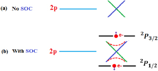
Figure 2. Orbital angular momentum of p -graphene state (l = 1) with (a) no coupling and (b) coupling with its spin intrinsic momentum.
Download figure:
Standard image High-resolution imageThe special relativity theory states that for electrons with large average speeds the mass increases, while the radius decreases. In the weakly relativistic domain, the SOC effect is specially noticed for massive atoms of the periodic table. There are some early studies [59, 60] indicating splitting of electron and hole energy bands by spin–orbit coupling (SOC) in 2D-GaAs heterostructures. Pyykkö [82] compared the relativistic (Dirac) and nonrelativistic (Schrodinger) dynamics for the valence electron in a given atomic potential, to study the importance of the direct relativistic effect on atomic orbitals. They found a relativistic radial contraction and energetic stabilization for s and p shells, spin–orbit splitting and the relativistic radial expansion and energetic destabilization of the d and all f outer shells. They also reported that all three effects were of the same order of magnitude and grew roughly as Z2.
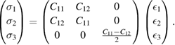
In order to study some mechanical properties that give physical insights into the potential aplications of a graphene/GaAs bilayer in engineering science, we calculated its C11, C12, C22 and C66 elastic constants. Due to hexagonal symmetry (C11 = C22 and (C11 − C12)/2 = C66), only two independent elastic constants C11 and C12 are considered in the stress-strain relation. Therefore, the Hooke's law ( = Cij
= Cij  , where
  and
and  , represent the stress and strain, respectively, and i, j are integers) for 2D hexagonal materials can be expressed in the matrix form [83]:
The Poison's ratio  , the in-plane Young's modulus Ys, the 2D layer modulus
  and shear
  modulus are obtained from the calculated C11 and C12 elastic constants, and multiplied later by the corresponding optimized unit-cell z distance. Their respective equations are [84, 85]:


The calculated elastic constants and the above mentioned mechanical properties for graphene and 2D-GaAs monolayers, as well as for the graphene/GaAs bilayer, are depicted in table 2. The Poisson's ratio represents the plasticity of the material, the 2D layer modulus gives physical insight about the resilience of a material to stretching, and the shear and in-plane Young's moduli indicate the 2D structure stiffness. Gonzalez et al [24] reported for 2D h-IIIAs binary compounds that as moved down in group III of the periodic table, the bond length between the neighboring cation-anion atoms increases and the materials display less stiffness and more plasticity.
Table 2. Calculated 2D Poisson's ratio ( ); Young's (Ys), layer (
 ), and shear (
 ) moduli for 2D graphene and GaAs monolayers, and the graphene/GaAs bilayer.
| C11 (J m−2) | C12 (J m−2) |  |
YS (J m−2) |  (J m−2) (J m−2) |
 (J m−2) (J m−2) |
|
|---|---|---|---|---|---|---|
| Graphene | 352.8 | 62.8 | 0.18 | 341.7 | 207.8 | 145.0 |
| 352.7 [85] | 60.9 [85] | 0.17 [85] | 342.2 [85] | 206.6 [85] | 145.9 [85] | |
| 2D-GaAs | 49.6 | 16.1 | 0.32 | 44.4 | 32.9 | 17.1 |
| — | — | 0.35 [25] | 48.0 [25] | — | — | |
| 551-graphene/ 331-GaAs | 384.7 | 70.0 | 0.18 | 372.1 | 227.4 | 157.0 |
3. Results and discussion
3.1. Structural properties and dynamical stability
Honeycomb unit cells of graphene and 2D-GaAs monolayers are shown in figures 1(a) and (b). Graphene monolayer displays a planar geometry while 2D-GaAs presents a buckled one. The TS-vdW optimized parameters for graphene and 2D-GaAs hexagonal monolayers, as well as for graphene and 2D-GaAs within a bilayer heterostructure (figure 1(c)), are shown for comparison in table 1. Our results for 2D-GaAs and graphene monolayers are in good agreement with previous theoretical results reported by DFT. The lattice parameter value of graphene monolayer is 39.1% shorter than that of 2D-GaAs monolayer. Using a computational method Kumar et al reported that lattice mismatch between two different bilayers causes elastic strains, which significantly affects their electronic properties [86]. In order to reduce this mismatch, a 551-graphene and 331-GaAs geometries were chosen, resulting in just 1.49% mismatch between graphene and GaAs sheets.
The vdW interlayer interaction between 551-graphene and 331-GaAs layers reduces the laticce constant of graphene by 0.24% and increases that of the GaAs by 1.01% compared to the respective values from pristine monolayers. As a result, the initial mismatch between 551-graphene and 331-GaAs is reduced from 1.49% to 0.18%, which increases the mechanical and dynamical stability of our system, as will be shown in the next sections. The optimized DFT-TS interlayer spacing (dL) between 551-graphene and 331-GaAs sheets is 3.476  . This value is higher than 3.34
  found for graphene-h-BN bilayer [49], and reasonably comparable to 3.40
  of 551-graphene/441-MoS2 heterostructures [87]. The interlayer distance is sensitive to the vdW flavour used in the calculatations. So, the correct vdW flavour choice is of vital importance [87]. Singh et al reported that the Tkatchenko–Scheffler method effciently evaluates the long-range vdW interactions and accurately predicts interlayer spacing between 551-graphene and 441-MoS2 sheets [87]. Their reported interlayer distance agrees with the experimental one (3.40
  ) [88]. On the other hand, theoretical [25, 26] and experimental [27] research has predicted and validated the stability of 2D buckled single layer of group III–V materials with ionicity. Al Balushi et al experimentally reported that graphene plays a critical role in stabilizing ionic 2D buckled group III–V structure. Their results provide a foundation for the discovery and stabilization of 2D group III–V materials that are difficult to prepare via traditional synthesis [27]. Using Bader analysis [89], we found a charge transfer of 5.3 electrons from Ga to As in the 551-graphene/331-GaAs bilayer, indicating a significant ionicity in the interplanar binding. However, no charge transfer from Ga to C atoms was found.
Figure 3 depicts the calculated phonon dispersion for the studied graphene/GaAs bilayer. It proves stability of the studied system, since there are no imaginary frequencies in the phonon dispersion. Some negative frequencies near  point are visible as well. This feature has been found in other 2D-systems [33, 87, 90–92] and highlights the flexural acoustic mode of 2D-systems. They are often present in the theoretical calculations due to inadequate numerical convergence close to
  point [87].
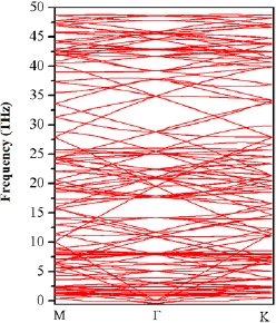
Figure 3. Phonon dispersion for the studied graphene/GaAs bilayer heterostructure.
Download figure:
Standard image High-resolution image3.2. Electronic structure and mechanical properties
The vdW-TS + SOC electronic band structure for the unstrained 551-graphene/331-GaAs bilayer (X = 0.0%) is displayed in figure 4. The brown lines represent the contributions of Ga-4s and As-4p z orbitals, while the green lines show the contribution of C-2p z orbitals. One can see the semiconductor  -
- direct nature for 331-GaAs layer, with a bandgap of 0.72 eV, and a near semimetallic nature with a tiny bandgap of 5.0 meV at K point for 551-graphene layer (highlighted in the inset of figure 4). This electronic behavior for 331-GaAs (
 -
- direct) is different from the one reported for 2D-GaAs monolayer (
 -K indirect) [24, 25]. Thus, the presence of graphene on GaAs layer induces an indirect to direct bandgap transition on GaAs layer, useful for optoelectronic applications and field-effect transistors. This bandgap transition can be physically explained by the vdW interaction between the localized C-2p z and As-4p z orbitals at K point, which shifts the latter orbital downward from the valence band maximum (VBM). Singh et al [87] reported that MoS2 undergoes a direct to indirect bandgap transition in 441-graphene/331-MoS2 bilayer heterostructure, whereas in 551-graphene/441-MoS2 bilayer it retains a direct bandgap nature. Authors stated that these bandgap transitions, when changing the layer geometries, are imposed by the level of strain intensity between the layers. Lattice mismatch between two different bilayers causes elastic strains, which significantly affects their electronic properties [86]. The change from indirect to direct bandgap nature of 2D-GaAs in our case is physically important because heterostructures can present high photoluminescence [87]. On the other hand, we found that the effects of GaAs and SOC open a bandgap of 5.0 meV at Dirac point in graphene within a graphene/GaAs bilayer. Our result agrees with those found for graphene/BN, where it has been reported that strain opens the bandgap in the range of 4 meV to 14 meV [93, 94]. Singh et al found that the SOC and proximity effects of MoS2 open a direct band gap in graphene of 0.4 meV and 1.1 meV for different graphene/MoS2 geometries [87].
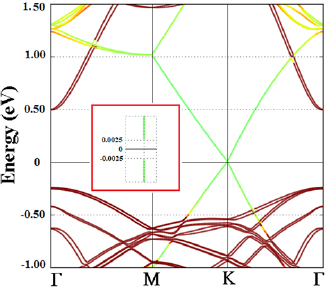
Figure 4. Electronic band structure for the studied graphene/GaAs bilayer, unstrained (X = 0.0%). The brown lines represent the contributions of Ga-4s and As-4p z orbitals, while the green lines show the contribution of C-2p z orbitals. The inset displays the bangap opening at Dirac point for graphene.
Download figure:
Standard image High-resolution imageThe elastic constants for graphene and 2D-GaAs monolayers, as well as for the studied graphene/GaAs bilayer system, are tabulated in table 2. Our results for the monolayer constituents of graphene/GaAs are in excellent agreement with those reported in previous theoretical and experimental studies. It is noteworthy that C11 > 0 and  , which means that all our systems satisfy the Born stability criteria [95] for mechanically stable 2D hexagonal structures. The calculated Poisson's ratio for 551-graphene/331-GaAs bilayer is smaller than (equal to) that of 2D-GaAs (graphene) monolayer. On the contrary, the 2D Young's (Ys), layer (
 ), and shear (
 ) moduli for bilayer heterostructure are higher when compared to those of its constituent monolayers. Therefore, 551-graphene/331-GaAs is a stronger material than graphene but with same plasticity, which makes it attractive for potential applications in engineering sciences.
3.3. Tuning graphene and 2D-GaAs bandgaps
Stress applied on heterostructure materials changes the interatomic distances and the relative positions of the atoms, which influences the electronic structure with potential optical applications [96]. Therefore, we have investigated the electronic properties of graphene and GaAs in graphene/GaAs bilayer hetrostructure under uniaxial stress along c axis and different planar strain distributions.
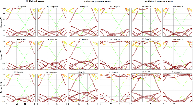
In order to study the effect of uniaxial stress along c axis on electronic properties of 551-graphene/331-GaAs bilayer the equilibrium interlayer distance between 551-graphene and 331-GaAs layers was modified by X = −6.0%, −4.0%, −2.0%, +2.0%, +4.0% and +6.0%. During each expansion (X > 0) and compression (X < 0), the vertical coordinate was kept fixed at each separation while atoms were allowed to relax in the plane of layers. Figure 5(i) displays the electronic structures for all these configurations. For X = +2.0%, +4.0% and +6.0% expansion cases, the 551-graphene (331-GaAs) bandgap is opened by 26.0% (4.2%), 68.0% (8.3%) and 68.0% (5.6%).
Figure 5. Electronic structures for (i) uniaxial stress along c-axis, (ii) biaxial symmetric strain, and (iii) uniaxial asymmetric strain along perpendicular C–C bond for X = −6.0%, −4.0%, −2.0%, +2.0%, +4.0% and +6.0% configurations of 551-graphene/331 GaAs bilayer crystal heterostructure.
Download figure:
Standard image High-resolution image
For the uniaxial compression along c axis, the graphene (GaAs) bandgap increases from 7.3 meV (0.75 eV) to 9.4 meV (0.78 eV) as the strain is increased from −2.0% to −4.0% before decreasing to 5.2 meV (0.67 eV) for −6.0%. From the results found for the uniaxial strain along c axis, we can infer that interlayer distance plays an important role for tuning both the graphene and GaAs bandgap in graphene/GaAs heterostructure. The graphene bandgap opening could be attributed to the enhanced SOC of graphene due to proximity of the GaAs-buckled effective potential. Using first-priciples method, Youngbin et al [52] studied the effect of strain on the bandgap characteristics of MXene semiconductors, for applications in optical devices. They reported that this material experiences an indirect to direct band gap transition with variation of the bandgap size at a relatively small critical strain of about 2%.
When applying symmetric strain distribution, the system underwent in-plane biaxial stretching and compression of 2.0%, 4.0% and 6.0% from its optimized lattice parameter value. Then, the lattice structure was optimized, the lattice vectors were set to their strained values, while only the atomic coordinates were allowed to relax. Figure 5(ii) shows the band structure of the graphene/GaAs systems with X = −6.0%, −4.0%, −2.0%, +2.0%, +4.0% and +6.0% symmetric strain. We find that there is no bandgap opening around the Fermi level for graphene, with any strength of symmetrical tensile or compressive strain. Nevertheless, strain results in remarkable change of the GaAs bandgap width around the Fermi level. As shown in figure 5(ii), biaxial strain results in decrease in the GaAs bandgap width until becoming metallic, while compressive strain leads to increase of the GaAs bandgap.
In the case of asymmetric strain distribution, graphene/GaAs bilayer supercell undergoes uniaxial stretching and compression in one direction, perpendicular to C–C bonds, of 2%, 4% and 6% from its optimized lattice parameter value, and remains unstrained along the other direction. Figure 5(iii) displays the electronic structures for X = −6.0%, −4.0%, −2.0%, +2.0%, +4.0% and +6.0% configurations. For X = +2.0% and +4.0%, the 551-graphene (331-GaAs) bandgap is opened (narrowed) by 267 and 541 meV (0.502 and 0.286 eV). As the expansion is increased to +6.0% the system becomes slightly metallic. For X = +2% and +4%, the graphene has a bandgap located at the left side of K point. For 6%, the bandgap is shifted to the K point. Gui et al found similar results for asymmetric strain distributions in graphene, though they reported direct and indirect graphene bandgap nature depending on the compression value [97].
On the other hand, figure 5(iii) shows that the graphene (GaAs) bandgap width increases to 91 meV (0.95 eV), 248 meV (1.05 eV) and 814 meV (1.04 eV) for X = −2.0%, −4.0% and −6.0%, respectively. We also note that GaAs bandgap preserves its direct nature at  point. Gui et al reported that for the asymmetric strain distribution perpendicular to C–C bonds in graphene, the bandgap increases from 0 to 170 meV as the strain increases to 4.91% [97]. The authors reported that the lattice symmetry breaking results in graphene bandgap opening at the Fermi level. From figure 5(iii) one notices that the valence-band maximum for GaAs is shifted upward, closer to the Fermi level as the compression increases, while the graphene valence-band maximum is shifted downward, farther from the Fermi level. One physical reason for this is that as the compression reaches a value larger than 4%, the repulsion between the charge accumulation around C atoms becomes stronger so the p -C orbitals are shifted downward farther from the Fermi level. For the case of GaAs, as the compression increases, due to the electronegative difference between their atoms, the attraction between the charge accumulation around Ga and As atoms becomes stronger so the GaAs orbitals are shifted near each other.
4. Conclusions
DFT-vdW–Tkatchenko–Scheffler method and spin–orbit coupling have been used to investigate the electronic band structures of 2D-GaAs and graphene monolayer constituents in graphene/GaAs bilayer heterostructure using a 551/331 supercell geometry. It was found that 2D-GaAs bandgap nature changes from  -K indirect in isolated monolayer to
  -
- direct in a bilayer heterostructure. This bandgap transition can be physically explained by the vdW interaction between the localized C-2p z and As-4p z orbitals at K point, which shifts this latter orbital downward of the valence-band maximum. The uniaxial stress along c-axis strongly influences the graphene electronic bandgap. The interlayer distance plays an important role for tuning both the graphene and GaAs bandgap in graphene/GaAs bilayer. The graphene bandgap opening could be attributed to the enhanced SOC of graphene due to proximity of the GaAs-buckled effective potential.
  -
- direct bandgap of 2D-GaAs in 551-graphene/331-GaAs is not altered as interlayer distance is varied. These are extremely important findings for potential optical applications by strain engineering. Symmetric in-plane strain does not open the graphene bandgap. Nevertheless, it induces remarkable changes in the GaAs bandgap width around the Fermi level. When applying asymmetric in-plane strain to graphene/GaAs, the graphene sublattice symmetry is broken, and the graphene bandgap is open at the Fermi level to a maximum width of 814 meV. We can conclude that the nature for both GaAs and graphene electronic band structures strongly depends on its lattice symmetry. The lattice symmetry breaking results in graphene band-gap opening at the Fermi level. These findings are important to enable tailoring the electronic properties of 551-graphene/331-GaAs heterostructure by strain engineering, for potential optical aplications. Phonon dispersion and elastic constants analysis display, respectively, the dynamical and mechanical stability of 551-graphene/331-GaAs bilayer vdW-heterostructure. The calculated 2D Young's (Ys), layer (
 ) and Shear (
 ) moduli for bilayer heterostructure are higher than those of its monolayer constituents, which indicates that our studied bilayer material displays more in-plane stiffness than its monolayer constituents. All together, our findings clearly indicate the feasibility of enhancing the physical characteristics of potential graphene-based group-IIIV optoelectronic devices by science engineering.
Acknowledgments
This work has been carried out with the financial support of Universidad del Norte and Colciencias (Administrative Department of Science, Technology and Research of Colombia) under Convocatoria 712—Convocatoria para proyectos de investigación en Ciencias Básicas, año 2015, Cod: 121571250192, Contrato 110-216; and the partial support of DGAPA-UNAM project IN114817-3. The authors gratefully acknowledge the support from the High Performance Computing core facility CalcUA and the TOPBOF project at the University of Antwerp, Belgium; DGTIC-UNAM under project LANCAD- UNAM-DGTIC-150, and the computing time granted on the supercomputer Mogon at Johannes Gutenberg University Mainz (hpc.uni-mainz.de).
Conflicts of interest
There are no conflicts to declare.