

Abstract
Etching of the cathodes in magnetron sputtering determines the plasma discharge properties and deposition efficiency. In high-power and high-ionization discharges, etching becomes more complicated, resulting in inaccurate results if the conventional models are still used. This work aims at establishing an accurate dynamic model for high-power and high-ionization discharges by combining the cellular automata (CA) method and particle-in-cell/Monte Carlo collision (PIC/MCC) method, in which all the interactions pertaining to the etching morphology, plasma density, electric field, and magnetic field are considered. In high-power discharges such as continuous high-power magnetron sputtering (C-HPMS), strong self-sputtering and intense gas rarefaction stemming from the high temperature in the vicinity of the target influence the etching behavior. Compared to the experimental results, the morphology simulated by the dynamic etching model shows an error of only 0.8% in C-HPMS, which is much less than that obtained by the traditional test-electron Monte Carlo (MC) method (10.1%) and static PIC/MCC method (4.0%). The dynamic etching model provides more accurate results to aid the development and industrial application of HPMS.
Export citation and abstract BibTeX RIS
1. Introduction
Magnetron sputtering [1] is widely used in large-scale fabrication of industrial coatings. In this process, etching of the cathode not only influences the plasma discharge [2] and target utilization [3], but also determines the coating uniformity and deposition efficiency [4]. In order to meet the increasing industrial demand, high power and ionization rates are demanded for magnetron sputtering, but the cathode etching behavior, coating quality, and process stability are more complicated and unpredictable.
To investigate the cathode etching phenomenon, experiments are usually conducted to correlate the etched morphology of the cathode with different discharge parameters such as the voltage [5], gas pressure [6], magnetic field [7], and ion properties [8], and the Yamamura equation [9] is usually adopted to calculate the ion sputtering yield. However, since trial-and-error experiments are prone to high cost and long validation time/cycles [10], accurate models are needed to predict the cathode etching behavior in magnetron sputtering. For example, the direct simulation Monte Carlo (DSMC) model [11] can be used to calculate the movement and collision of neutral particles, so that the etching morphology can be mapped by determining the distribution of ions that sputter the target. Normally the plasma and neutral particles are assumed to be uniformly distributed in the background [12] and the type and probability of collisions are space independent thus giving rise to poor simulation accuracy [13]. In comparison, the test-electron Monte Carlo (MC) model [14] can yield the plasma discharge state by calculating the electron movement under the electromagnetic field and consequently the etching morphology. However, the test-electron MC model oversimplifies the ion sputtering process on the target [15] and neglects the self-consistent potential of the plasma [16]. In view of these shortcomings, self-consistent plasma models such as the fluid model [17] and particle-in-cell/Monte Carlo collision (PIC/MCC) model [18] have been proposed. The former can simulate the plasma density distribution and calculate the sputtering ion flux on the target [19], but ignores the properties and states of the incident ions [20]. Besides, it cannot be used in a strong magnetic field or with complex boundary conditions [20]. The PIC/MCC method overcomes the disadvantages of the fluid model [21], and further introduces the effects of different factors such as the temperature [22], pressure [23] and voltage [18] to provide accurate prediction of etching in the initial stage [18, 21–23]. However, since the electric and magnetic field distributions on the target change with etching, the plasma discharge state changes gradually, consequently resulting in worse accuracy in the latter discharging stage [24]. In particular, high-power magnetron sputtering (HPMS) [25] which adopts a high ionization rate changes the plasma discharge behavior and ion-surface interactions [26], resulting in significant differences in the results obtained by conventional static etching simulation and experiments. Besides, intense self-sputtering and high temperature caused by the high-power discharge decrease the simulation accuracy of the traditional PIC/MCC model.
In this work, a high-precision dynamic etching model combining the traditional PIC/MCC model and cellular automata (CA) method [27] is established to deliver more accurate results. The physical processes in the plasma discharge and cathode etching in HPMS are analyzed and the influence of self-sputtering and high temperature on the plasma discharge and cathode etching is studied. Experimental results reveal a simulation error of only 0.8% that is much better that obtained by the traditional test-electron Monte Carlo (MC) method (10.1%) and static PIC/MCC method (4.0%) for continuous HPMS (C-HPMS) [28].
2. Methods
The software package used in our simulation is commercial software MATLAB R2019b. According to the detailed flowchart shown in figure A1, the codes of the models (including PIC/MCC model, test-particle MC model, CA model, dynamic etching model and ionization region model) are self-developed based on the function module of MATLAB [28, 29]. During the simulation, the models invoke several built-in functions of MATLAB, including matrix operations, linear interpolation, ordinary differential equations, data reading and storage, post-processing, program loop and judgment. The programs are performed on the high-performance computing clusters (Intel(R) Xeon(R) CPU E5-2650 v3 @ 2.30 GHz) with 10 cores, which could significantly improve the computational efficiency.
2.1. Plasma discharge simulation
The schematic diagram of the magnetic field distribution and simulation domain in the PIC/MCC model is depicted in figure 1. Since the straight part of the race track is much longer than the corner, the rectangular planar magnetron sputtering cathode can be visualized as a two-dimensional plane. According to the geometric symmetry, the simulation domain is simplified to half of the actual area. In this work, the maximum of the electron density ne is about 1 × 10¹⁹ m−3, and the electron plasma frequency ωpe is about 1.8 × 10¹¹ Hz calculated by  (e= 1.6 × 10⁻¹⁹ C,
  0 = 8.85 × 10⁻¹² F m−1 and me = 9.1 × 10⁻³¹ kg) [30]. Therefore, the time step is set to 1 × 10⁻¹² s, which is smaller than 1/5/ωpe = 1.1 × 10⁻¹² s [31]. The grid size is below the electron Debye length all the time. In order to reduce the computation, the grid size is dynamically changing with the increase of the plasma density and the consequent decrease of the electron Debye length. In detail, at the beginning of the discharge, the plasma density is 1 × 10¹⁴ m−3, so the electron Debye length λDe is about 1.2 mm calculated by
  (Te = 2.5 eV) [30]. The simulation domain is divided into uniform square grids with a length of 0.5 mm, smaller than 1.2 mm. The program will check the Debye length every 10 time-steps. Once the grid size is larger than the Debye length, it will reduce to a smaller value. At last, the grid size depends on the plasma density whatever in time or in space. By this way, the dimension of sparse matrix is effectively reduced when calculating Poisson's equation, resulting in a significant improvement of the computational efficiency. In addition, the electron average velocity in this work is about 1 × 10⁶ m s−1 (Te = 2.5 eV). Therefore, the test-electron travels about 1 μm in each time-step, which is less than the grid size [32].
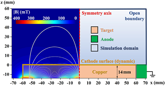
Figure 1. Schematic diagram of the magnetic field distribution and simulation domain.
Download figure:
Standard image High-resolution imageThe Cu target of the cathode has a width of 120 mm and thickness of 14 mm and the maximum etching depth is 12 mm. The discharge occurs in the Ar atmosphere at a pressure of 1.0 Pa. The anode is grounded and the cathode potential is −700 V. In the Ar/Cu discharge system, the main particles include electrons (e), ground state atoms (Ar and Cu), metastable atoms (Arm), and ions (Ar+ and Cu+). The initial plasma density is set to 1 × 10¹⁴ m−3 and each test particle (super-particle) represents 1 × 10⁷ actual particles in the simulation. 34 320 electrons and Ar+ are randomly generated in the simulation domain according to the grid quantity and their initial velocities are predicted by the Maxwellian distribution [28]. The initial average ion temperature is assumed equal to the background temperature, which is calculated by the plasma heat transfer model [33]. The initial average electron temperature is 2.5 eV in C-HPMS according to Chen et al [28]. The initial density of Cu is 0, and Cu atoms are generated by sputtering accompanied by secondary electron emission. The sputtering yield is calculated by TRIM [34] as shown in figure A2 and the secondary electron emission coefficient γ is calculated by equation (1) [30]:

where Eiz (eV) is the ionization energy of the sputtering ions and ϕ (eV) is the electronic work function of the target materials. The main reactions in the Ar/Cu discharge are listed in table 1 but Penning ionization and Cu+ secondary ionization are ignored [30]. The collision probability Pcoll of the reactions is determined by equation (2):

Table 1. Main reactions in the Ar/Cu plasma.
| No. | Reactions | Threshold (eV) | Type | References |
|---|---|---|---|---|
| 1 | e + Ar → Ar+ + 2e | 15.76 | Ionization | [37] |
| 2 | e + Ar → Arm + e | 11.56 | Excitation | [37] |
| 3 | e + Arm → Ar + e | −11.56 | De-excitation | [37] |
| 4 | e + Arm → Ar+ + 2e | 4.2 | Ionization | [37] |
| 5 | e + Ar → e + Ar | — | Elastic collision | [30] |
| 6 | Ar + Ar+ → Ar + Ar+ | — | Elastic collision | [30] |
| 7 | Ar + Ar+ → Ar+ + Ar | — | Charge exchange | [30] |
| 8 | e + Cu → Cu+ + 2e | 7.68 | Ionization | [38] |
| 9 | Cu + Ar+ → Cu+ + Ar | — | Charge exchange | [39] |
| 10 | Cu + Cu+ → Cu+ + Cu | — | Charge exchange | [40] |
| 11 | Cu + Cu+ → Cu + Cu+ | — | Elastic collision | — |
where N0 (m−3) is the density of neutral particles and σ (m2) is the collision cross section of the reactions.  m s−1 is the particle velocity and (eV) is the particle energy. The collision cross section of electrons is determined by the electron energy according to Lennon et al [35]. Collisions between the ions and atoms are treated as hard ball collisions [30] with the cross section described by equation (3):

The ionic radius Ri is assumed to be equal to the atomic radius Ra. The atomic radii of Ar and Cu are 1.88 × 10⁻¹⁰ and 1.4 × 10⁻¹⁰ m, respectively [36].
The simulation domain contains three types of boundaries, namely the open boundary (including anode boundary), symmetrical boundary, and cathode boundary. The super-particles disappear directly at the open boundary and rebound at the symmetrical boundary. At the cathode boundary, electrons disappear directly, while target sputtering and emission of secondary electrons occur when ions impinge onto the target. The self-consistent potential of the plasma is calculated by Poisson's equation for each step. To optimize the speed and stability in the calculation, the maximum of the super-particles is set to 1 × 10⁶ and when the number of super-particles exceeds the maximum, it is halved and the weight doubled [41]. The the steady state is defined once the convergences of the potential and the electron density are obtained [42, 43], like figure A3.
2.2. Ion sputtering simulation
According to the steady-state plasma density distributions obtained by PIC/MCC simulation, a large number of test ions are generated randomly, including Cu+ and Ar+, which are the initial conditions in the test-ion MC model. The etching flux is derived by calculating the ion movement at the steady state potential and magnetic field. To increase the calculation speed while maintaining the calculation accuracy, the time step is set to 1 × 10⁻⁸ s to ensure that the motion distance of ions is smaller than the grid length. At each step, a random number Rcoll is generated to determine the collision information between ions and neutral atoms in the background. If Rcoll is larger than the sum of the elastic collision probability Pel and charge exchange probability Pex, no collision occurs for the ions. If Rcoll < Pel, elastic collision occurs and the ion velocity is calculated according to momentum conservation and energy conservation [30]. If Pex < Rcoll < Pel + Pex, charge exchange collisions occur and the collided atom is set as a new test ion with the thermal velocity. According to the sputtering energy and angle of incident ions at the target, the sputtering yield Y is calculated by TRIM [34]. Assuming that n ions sputter at a certain position x (x-coordinate) on the target, the etching flux Γx is equal to the sputtering yield caused by all the ions, as shown in equation (4):
2.3. Etching morphology simulation
The etching morphology is simulated by the CA method [27] as shown in figure A4. The target and discharge region are divided into a series of cells. To simultaneously increase the calculation speed and maintain the accuracy, the cells are set to 0.5 mm × 0.5 mm. The volume fraction of the target atoms in each cell is defined as the filling value C and describes the etching degree of each cell. A filling value of 1 (100%) initially means that the solid cells are filled with the target atoms before sputtering. After sputtering commences, it decreases and becomes an empty cell (C = 0) eventually. At this time, the cell becomes the discharge region from the original target region. The etching flux is normalized by refreshing the filling value of the solid cells using equation (5):

where the subscripts x and z represent the coordinates of the cell center and the subscripts 0 and t represent the initial and the final value of the filling value C, respectively. Ax
= Γx
/max(Γ) is the normalized etching flux and if  , the next cell will be etched. The target atoms are assumed to be etched uniformly and continuously in each cell. After etching in each step, the height hx,z
of remaining target atoms in the etched cell is simplified by equation (6):
, the next cell will be etched. The target atoms are assumed to be etched uniformly and continuously in each cell. After etching in each step, the height hx,z
of remaining target atoms in the etched cell is simplified by equation (6):

where Δl = 5 mm is the side length of the cells and  is the final filling value. According to figure A4, the remaining target height Hx
at position x is described by equation (7):
is the final filling value. According to figure A4, the remaining target height Hx
at position x is described by equation (7):
In this way, the etching morphology in each etching cycle is obtained by relating Hx at each location x as shown by the blue line in figure A4.
2.4. Dynamic etching
The flowchart of the entire dynamic etching simulation is displayed in figure A1. To ensure good accuracy, the cathode boundary is updated after 1 mm of the target is etched and the plasma discharge is derived again by the PIC/MCC model based on the new cathode boundary. Meanwhile, the simulation domain becomes irregular because of the changing cathode boundary and so the spatial potential is obtained by the ghost fluid method modified Poisson's equation [30]. Based on the new plasma density and electric field, another etching cycle yields a new etching profile. In this way, the discharge-etching cycle continues until a total etching depth of 12 mm. To improve the computational efficiency, the plasma density and spatial potential simulated at (d-1) mm will be set as an initial value to the next calculating of the plasma discharge at etching depths d mm (1 ⩽ d ⩽ 12).
2.5. Discharge experiments
Discharge experiments were performed on a homemade vacuum chamber with a diameter of 1200 mm and height of 1350 mm. A custom high-power cathode was used for the C-HPMS [28] discharge in the constant current mode (I= 35 A) sustained by a 60 kW DC power supply (Ascent 60 K, Advanced Energy, US) with a maximum output voltage of 1000 V and maximum output current of 60 A. The cathode target was Cu (99.9% pure, 600 × 120 × 14 mm3) and the background pressure was 5.0 × 10⁻³ Pa. The working gas was Ar (99.999% pure) and discharge pressure was 1.0 Pa. A Vernier caliper was employed to measure the etching morphology.
3. Results and discussion
Figure 2 presents the distributions of the plasma densities, spatial potentials, target magnetic fields, and etching fluxes at different etching depths (d= 0, 4, 8, and 12 mm) calculated by the dynamic etching model for 700 V and 1.0 Pa. With etching, the target surface concaves gradually producing an approximately circular arc morphology as revealed by the white curves. Correspondingly, the plasma density increases gradually (figure 2(a)) and the steady peak increases from 8.5 × 10¹⁸ m−3 (d= 0 mm) to 1.3 × 10¹⁹ m−3 (d= 12 mm). The discharge region with high intensity (plasma density > 8 × 10¹⁸ m−3) is larger, implying that the plasma discharge is significantly enhanced during etching. The thickness of the sheath decreases gradually (figure 2(b)) because of the enhanced discharge, which reduces the collision probability of the sputtering ions in the sheath. Consequently, the energy loss of the sputtering ions diminishes, resulting in a higher average sputtering energy (figure A5) and larger sputtering yield according to figure A2. The magnetic field intensity (figure 2(c)) on the target increases with etching which enhances electron confinement and promotes ionization. Therefore, the plasma discharge region becomes larger gradually during etching. Three peaks with larger values appear in the tangential magnetic induction intensity and a wider discharge region is observed. The etching width of the target increases gradually from 48 mm (d= 0 mm) to 56 mm (d= 12 mm) as shown in figure 2(d). Three zero points (Bn = 0, marked as a purple star in figure 2(c)) are found from the normal magnetic field intensity on the target and the distance between each zero points increases with etching. Previous results [44] show that the fastest etching occurs at the zero points. Therefore, a smooth quadrangle can be obtained from the sharp peak in the etching curve (figure 2(d)) with etching indicative of more homogenous etching. According to equation (4), the etching flux is determined by the quantity and sputtering yield of sputtering ions. Therefore, the evolution of etching on the target is attributed to two reasons, the first being the larger number of sputtering ions as a result of the bigger plasma density (figure 2(a)) and the second being the higher average sputtering yield on account of the larger average sputtering energy.

Figure 2. Distributions of (a) plasma densities, (b) spatial potentials, (c) target magnetic fields, and (d) etching fluxes at different etching depths (d = 0, 4, 8, and 12 mm).
Download figure:
Standard image High-resolution imageFigure 3 compares the etching morphologies simulated by the dynamic etching model, test-electron MC model, and static PIC/MCC model at 700 V and 1.0 Pa. In the test-electron MC simulation, the electron density distribution is translated into the etching profile directly. Because the local high density of electrons is caused by the uneven magnetic field, the test-electron MC model shows the narrowest etching morphology with a half width of 14.8 mm. In comparison, the etching morphology can be proportionally translated from the etching flux at 0 mm (figure 2(d1)) obtained by static PIC/MCC model, which involves the self-consistent potential and ion sputtering process. Therefore, the tangential component of the spatial electric field and collisions between ions and background atoms further widen the ion distribution, resulting in a wider etching flux. Hence, the etching morphologies calculated by the static PIC/MCC model are wider with a half width of 22.1 mm. Based on the traditional static PIC/MCC model, the dynamic etching model further incorporates the interactions of the etching morphology, plasma density, electric field, and magnetic field. When the etching depth is small (d = 2 mm), the interaction is weak and consequently, the dynamic etching model shows an etching morphology basically consistent with that generated by the static PIC/MCC model with a half width of 22.8 mm. However, when the target etching depth increases to 12 mm, the interaction is stronger and the changing target etching morphology leads to a higher magnetic field, enhanced plasma discharge, as well as wider sputtering flux in etching. Therefore, the etching morphology calculated by the dynamic etching model becomes wider exhibiting a half width of 24.4 mm.
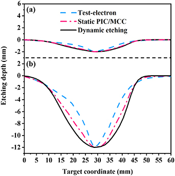
Figure 3. Etching morphologies derived by the test-electron MC model, static PIC/MCC model, and dynamic etching model at etching depths of (a) 2 mm and (b) 12 mm for 700 V and 1.0 Pa.
Download figure:
Standard image High-resolution imageIn high-power discharges and sputtering, self-sputtering is enhanced significantly compared to the low-power processes [45] and the number of sputtering ions varies from Ar+ to metallic ions. Hence, the target current composition in the high-power (C-HPMS) and low-power (dcMS) discharges are analyzed by the ionization region model [45] before simulation of target etching in C-HPMS, as shown in figure 4. The voltage–current characteristics of the Ar/Cu DC discharge are measured as the input of the ionization region model, as shown in table 2. The target current composition at low power (0.34 kW, power density <1 W cm−2, marked as the blue pentagon) is shown in the yellow region. The ratio of the primary gas current Iprim to the total discharge current ID is about 0.90, suggesting that most of the sputtering ions are Ar+. In comparison, the target current composition in the high-power discharge (21 kW, power density is 37 W cm−2, marked as the red star) in Region A reveals that self-sputtering dominates in the high-power discharge (C-HPMS). The ratio of the self-sputtering current ISS to the total discharge current ID is 0.82 and therefore, most of the sputtering ions are Cu+. Here, divalent Cu2+ ions are neglected [29] because the secondary ionization energy of Cu is much larger than the primary ionization energy [30]. Moreover, secondary electron emission from the target is negligible due to the small secondary electron emission coefficients of Ar+ (0.112) and Cu+ (0) [30]. Therefore, the total target current ID (A) is the sum of the ion currents of Ar+ and Cu+ as shown in equation (8):

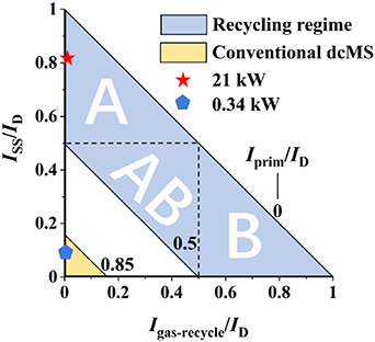
Figure 4. Recycling current ratio map: regions A, B, and AB are the SS-recycle dominated, gas-recycle dominated, and mixed-recycling ranges, respectively.
Download figure:
Standard image High-resolution imageTable 2. Voltages and currents in the Ar/Cu DC discharge at high and low power settings.
| Power (kW) | Voltages (V) | Currents (A) |
|---|---|---|
| 21 | 710 | 30 |
| 0.34 | 344 | 1 |
where e= 1.6 × 10⁻¹⁹ C is the charge of sputtering ions, S (m2) is the sputtering area on the target, and  and
and  m−2−s–1 are the sputtering fluxes of Ar+ and Cu+, respectively. Assuming that ions leave the ionization region with the Bohm velocity vB (m s−1) [30], the sputtering flux can be expressed by equation (9) [37]:
where  and
and  (m–3) are the densities of Ar+ and Cu+,
  and
and  (kg) are the masses of Ar+ and Cu+, respectively, and Te (V) is the electron temperature. Assuming that the proportion of the self-sputtering current in the system is k= ISS/ID, the ion proportions of Ar+ (
 ) and Cu+ (
 ) can be determined by equation (10):
C-HPMS shows significant heat accumulation because of the high-power discharge [46]. Generally, the temperature is below 800 K in dcMS [47] but can increase to 1000–2000 K to produce a large gradient in the ionization region in C-HPMS [48]. Hence, the plasma heat transfer model [33] is introduced to analyze the temperature distribution in the discharge region, as shown in figure 5. At a low power (0.34 kW), the temperature gradient is small and the average temperature in the discharge region is about 470 K. In comparison, at a high power (21 kW), the temperature gradient is larger and the average temperature exceeds 1500 K. According to Clapeyron equation, the density of the background gas N0 (m−3) is inversely proportional to the background temperature T (K) at pressure p (Pa) as shown in equation (11):
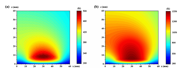
Figure 5. Temperature distributions in the discharge region at (a) low (0.34 kW) and (b) high power (21 kW).
Download figure:
Standard image High-resolution imagewhere R= 8.314 J mol−1·K−1 is the molar gas constant and NA = 6.02 × 10²³ mol−1 is Avogadro's constant. Therefore, N0 is smaller in the high-power discharge (C-HPMS) because the high temperature causes intense gas rarefaction [46]. Consequently, the collision probability of ions decreases according to equation (2) and the ion free paths increase giving rise to a wider etching range and smaller ion energy loss.
To explore the influence of self-sputtering and gas rarefaction by the dynamic etching model, cathode etching in dcMS (300 V) and C-HPMS (700 V) is determined by the original dynamic etching model, self-sputtering modified model, temperature-modified model and mixed modified model, as shown in figure 6. All the four models are based on the dynamic etching models. The difference is that the original model ignores the influence of the self-sputtering and the temperature, the sputtering ions are all Ar+ and the background temperature is set to 300 K. And the self-sputtering modified model introduces self-sputtering in the original model, where the sputtering ions are Ar+ and Cu+ with the ratio calculated according to figure 4. The temperature-modified model introduces temperature in the original model, where the gas density and the average energy are calculated according to the background temperature distribution shown in figure 5. The mixed modified model introduces both self-sputtering and temperature in the original model. In dcMS, the etching morphologies calculated by the modified models are similar to those derived by the original dynamic etching model. As shown in table 3, the differences in the half widths are very small, suggesting that the effects of self-sputtering and gas rarefaction are limited. However, in C-HPMS, significant differences can be found from the etching morphologies and there is significant dependence on self-sputtering and gas rarefaction. Generally, the incident angles of the sputtering ions are very small (<20° [49]) at the track center and the sputtering yield of Ar+ is larger than that of Cu+ as shown in figure A2. However, most of the sputtering ions are Cu+ in the self-sputtering modified model and so the half width of the etching morphology is only 21.9 mm and narrower than that calculated by the original etching morphology model. The ion incident angles increase near the race track edge (x< 12 mm and x> 43 mm) as shown in figure A6. According to figure A2, the sputtering yield of Cu+ increases faster with incident angles and exceeds that of Ar+ at about 50°. Therefore, compared with the original model, the edge region of the etching morphology calculated by the self-sputtering modified model is wider. In comparison, because of the high background temperature, gas rarefaction is very intense and decreases the collision probability, resulting in larger mean free paths and higher sputtering energy. Therefore, the etching morphology calculated by the temperature-modified model is wider with a half width of 28.4 mm. The mixed modification combines the effects of both self-sputtering and gas rarefaction. In the central region (12 mm < x < 43 mm), the etching morphology generated by the mixed modified model is slightly wider than that calculated by the original etching model because of the cancelation effect rendered by self-sputtering and gas rarefaction. In the edge region, the etching morphology determined by the mixed modified model is wider because of the combined effects of self-sputtering and gas rarefaction.
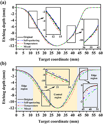
Figure 6. Target etching morphologies calculated by the original and modified dynamic etching models in (a) dcMS (300 V) and (b) C-HPMS (700 V).
Download figure:
Standard image High-resolution imageTable 3. Half widths of the etching morphologies calculated by the original and modified dynamic etching models in dcMS (300 V) and C-HPMS (700 V).
| Voltage | Original | Self-sputtering | Temperature | Mixed |
|---|---|---|---|---|
| 300 V | 27.9 mm | 27.5 mm | 28.6 mm | 28.1 mm |
| 700 V | 24.5 mm | 21.9 mm | 28.4 mm | 25.6 mm |
In order to verify the accuracy of the dynamic etching model, a Cu target is used experimentally in the Ar atmosphere in C-HPMS as shown in figure 7(a). The glow is bright green suggesting the presence of a large number of Cu particles in the plasma and that self-sputtering is stronger than gas sputtering. The top view (figure 7(b)) and cross-sectional view (figure 7(c)) disclose that the etching morphology of the cathode is basically symmetrical and uniform. Four cross sections are selected randomly to calculate the average to represent the experimental etching morphology (black solid line in figure 8). The etching morphology simulated by the optimal (mixed modified) dynamic etching model in C-HPMS (21 kW, 700 V, 30 A) is basically consistent with the experimental etching morphology shown by the red dashed line. The simulated target utilization rate is about 41.5% and slightly larger than the experimental target utilization rate of 38.9%. Compared to the experimental etching morphology (half width = 22.8 mm), the simulated etching morphology is a little wider with the half width of 25.6 mm, but it is slightly narrower at x> 46 mm. This is because the experimental constant current (35 A) is larger than the model parameter (30 A) and self-sputtering is more intense in the experiments. Previous studies have shown that the target voltage has almost no effect on the etching morphology [50–52] and therefore, the model parameters are reset to the average voltage of 700 V and constant current of 35 A according to experiments. The new simulation results generated by the ionization region model [45] reveal that the experimental proportion of self-sputtering is ISS/ID = 0.89. Consequently, the new calculated etching morphology with a half width of 24.4 mm represented by the blue dotted line is closer to the experimental etching morphology. The target utilization rate decreases further to 39.7% and shows an error of only 0.8% compared to the experimental target utilization. In contrast, the target utilization rates calculated by the test-electron MC model and static PIC/MCC model in figure 3(b) are 28.8% and 34.9%, respectively, equivalent to errors of 10.1% and 4.0% which are much larger than that of the dynamic etching simulation. All in all, the dynamic etching model shows much improved accuracy in predicting the cathode etching behavior in HPMS.

Figure 7. C-HPMS experiments using a Cu target: (a) glow photograph; (b) top view and (c) cross-sectional view of the target etching morphology.
Download figure:
Standard image High-resolution image
Figure 8. Comparison of the etching morphologies obtained by experiments and the dynamic etching model.
Download figure:
Standard image High-resolution image4. Conclusion
In order to address the poor accuracy in predicting the plasma discharge properties and cathode etching phenomenon in HPMS, a dynamic etching model is established by combining the PIC/MCC model and CA method. The dynamic etching model incorporates the interactions among the etching morphology, plasma density, electric field, and magnetic field to provide more accurate simulation of the plasma discharge properties and cathode etching morphology. Simulation results obtained in C-HPMS and dcMS reveal that the influence of self-sputtering and gas rarefaction is more significant in HPMS. Self-sputtering increases the proportion of Cu+ in the sputtering ions, whereas intense gas rarefaction increases the mean free path and sputtering energy of the ions. The etching morphology calculated by the optimal model is highly consistent with experimental etching results in C-HPMS showing an error of less than 0.8%. In conclusion, the dynamic etching model improves the simulation precision significantly and is a valuable tool to study the dynamics of HPMS, especially at large etching depths. The results described in this paper also provide insights into the mechanism of HPMS and optimal hardware design.
Acknowledgments
This work was financially supported by the Shenzhen Science and Technology Research Grants (JSGG20191129112631389), Shenzhen–Hong Kong Research and Development Fund (No. SGDX20201103095406024), City University of Hong Kong Strategic Research Grant (SRG) (No. 7005505), Guangdong–Hong Kong Technology Cooperation Funding Scheme (TCFS) (No. GHP/085/18SZ), Peking University Shenzhen Graduate School Research Start-up Fund of Introducing Talent (No. 1270110273), and Shenzhen postdoctoral research fund project after outbound (No. 2129933651).
Data availability statement
All data that support the findings of this study are included within the article (and any supplementary files).
: Appendix

Figure A1. Flowchart of the entire dynamic etching simulation.
Download figure:
Standard image High-resolution image
Figure A2. Sputtering yields versus incident angle and sputtering energy of different ion species.
Download figure:
Standard image High-resolution image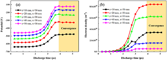
Figure A3. The temporal evolution of (a) the potential and (b) the electron density at different points.
Download figure:
Standard image High-resolution image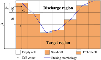
Figure A4. Schematic diagram of the cellular automata method.
Download figure:
Standard image High-resolution image
Figure A5. Ionic sputtering energy at different etching depths (d = 0, 4, 8, and 12 mm).
Download figure:
Standard image High-resolution image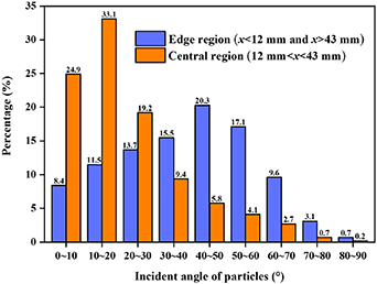
Figure A6. Probability distributions of ion incident angles.
Download figure:
Standard image High-resolution image