

Abstract
This study addresses the synthesis and mechanical behavior of graphene-metal composites comprising palladium (Pd) nanoribbons wrapped with graphene. Coating Pd nanoribbons with graphene by chemical vapor deposition (CVD) considerably increases their elastic modulus. These measurements are made by suspended microbridge indentation. A refined indentation measurement approach carefully takes into consideration the uncertainty resulting from the non-ideal bridge geometry. The measured composite moduli depend on the ribbon thickness in the range of 36–250 nm, with the maximum modulus of 147 GPa measured for 36 nm thick nanoribbons, representing an increase of 41.6% over uncoated Pd nanoribbons. The results clearly demonstrate that graphene, owing to its high modulus and strong interaction with Pd, can effectively reinforce Pd nanoribbons up to thickness of 250 nm, which corresponds to a volume fraction of 0.54%. We study the modulus scaling by deriving a mathematical rule of mixture model considering 3D 'bulk' metal nanoribbons reinforced by the 2D graphene 'surface'. This modeling approach is inspired by the framework of surface modulus, which is typically employed to explain the deviations in the moduli of nanowires and nanoribbons observed in the sub-10 nm regime. Here, the nanoribbons are much thicker, yet graphene's extremely high modulus leads to the observed increase in the measured composite moduli. Further, in these calculations, we consider the critical role of the nonlinear modulus component of graphene -its quadratic dependence on strain- which results from the lattice mismatch-induced interfacial strains between graphene and Pd. Graphene-Pd composite nanoribbons and thin films can be very useful for a wide range of application ranging from strain-engineered catalysis to damage tolerant flexible electronic devices. Beyond nanoribbons, the proposed 3D/2D rule of mixture model may be used to explain the modulus scaling in 3D/2D heterostructures and in bulk graphene-metal nanocomposites made by powder mixing routes.
Export citation and abstract BibTeX RIS
1. Introduction
Materials with reduced dimensions such as nanowires, nanotubes and ultrathin films are suitable for applications requiring folding and stretching, since the flexural rigidity decreases cubically with thickness [1]. By virtue of this stretchable geometry, ultrathin interconnects and electrical lines shaped like springs are finding applications in almost all novel flexible devices like flexible display, electronic textile, health care, human–machine interaction, to name a few [1–3]. It is hence important to understand the mechanical behavior of ultrathin film materials and more specifically, to design new thin films having precisely controlled elastic properties. Mechanical degradation or failure of thin metal connections in flexible electronics would lead to a shorter lifetime or make device vulnerable to complete failure. In addition to design complex stretchable wavy structures, ultrathin film materials mechanical property reinforcement may guarantee a device's long lifetime intrinsically. Strain-engineering of crystalline catalyst materials such as Pd is also another novel use of very thin films [4] where it is found that large compressive strains imparted due to interfacial energy can strongly tune the chemical reactivity.
It is well-established that materials often exhibit unusual mechanical behavior when the dimensions of the structure approach some critical length scale, typically below 10 nm. Wong et al have measured the elastic bending stiffness of SiC nanorods and multiwall carbon nanotubes (MWNTs) and observed spring force constant dependence on material diameters [5]. As for metals, Cuenot et al have measured the elastic moduli of silver and lead nanowires and noticed increase in the elastic modulus as the wire diameter decreases [6]. For hard materials like diamond, Banerjee et al recently demonstrated the increase in the elastic strain limit by 9% by shrinking diamond rod diameter to nanoscale [7]. These experiments provide direct evidence for what is known as 'scale effects' where the elastic properties of materials depend on size in the nanometer range.
Several mechanisms have been proposed to explain the variations observed in the elastic properties of crystalline materials at the nanoscale. It is now accepted that while the mechanical properties of materials at the micro- to macro scales are dominated by the 'bulk' elastic strain energy, surface effects including surface modulus, surface energy, residual surface stresses [6, 8, 9] and surface toughness [7] become more dominant and can significantly modify the elastic properties at the nanoscale. These ideas are typically put in context of the increase in surface-to-volume ratio at the nanoscale. It should be noted that surface elasticity of a solid body is the reversible work per unit area needed to elastically stretch a preexisting surface and is a function of -but not necessarily equal to- material's surface energy [10]. The surface modulus has been mathematically considered as a surface traction in a continuum sense to calculate the overall modulus of nanowires and nanoribbons which takes into consideration the bulk and surface moduli components [8].
The pursuit to use nanowires and nanoribbons with increased modulus in engineering applications has proved to be practically more challenging than originally anticipated. Crystals have relatively low surface energies, e.g. Ni (110): 2.44 Jm−2, Mo (110): 2.07 Jm−2, Si (110): 1.39 Jm−2 [11]. Consequently, the effect of surface modulus on nanowire moduli is typically significant only when the nanowires are < 10 nm. Specific to this study, Pd (110) has surface energy around 1.6 Jm−2 [11, 12] and its modulus is expected to have imperceptible thickness dependence when it is thicker than 10 nm [10]. This stringent requirement for extremely small -sub 10 nm- sizes to observe scale effects on the mechanical behavior of nanowires present a roadblock towards the engineering of materials which exploit surface effect for increased moduli. Simply put, these sub-10 nm nanowires and nanoribbons are significantly more challenging to synthesize, manipulate and stabilize for extended times.
In this work, we study a new route to reinforce metal nanoribbons by directly growing graphene on the surface. Graphene is a 2D surface of sp2-hybridized carbon atoms, has an extremely high in-plane mechanical stiffness [13]. Incorporating high quality graphene on the surface of metal films, or as laminated composite (also known as layered metal-graphene composites) is a promising way to exploit its properties for applications [14–16]. There is a strong need for establishing new understanding and design rules for the incorporation of 2D materials in new composites, and benchmarking their mechanical behavior. Mechanical behavior of materials is at the heart of most engineering applications due to reliability issues. However, this need is for basic understanding is not currently addressed, with most recent studies composites are made by top-down approach and incorporate highly disordered structures. As a result, this precludes clear understanding of the bounds of mechanical reinforcements in these materials. Our approach builds on our capabilities to synthesize high-quality graphene on the surface of ultrathin palladium (Pd) nanoribbons via a rapid Chemical Vapor Deposition (CVD) process, which has been developed in our previous study [17], and study the size dependent elastic modulus in palladium graphene (PdGr) composites. Graphene acts as an atomically thin but very stiff 'surface'. Perhaps not surprisingly, the modulus of PdGr is significantly increased compared to bulk Pd in the range of 36–250 nm. Effectively increasing the moduli of metal thin films, nanowires or nanoribbons with thicknesses up to >200 nm can be very significant for the engineering applications in flexible electronics, sensors, and smart textiles to name a few.
To measure the mechanical behavior of the composite nanoribbons, we develop a refined approach to account for uncertainties arising during the indentation of suspended microbridges. There are extensive studies on testing the mechanical behaviors of thin film materials when they are freestanding (or unsupported) [18, 19] or on substrates [20, 21]. Indentation measurements on a doubly-clamped microbridge have been successfully used to acquire the elastic and fracture properties of ultrathin materials like graphene ribbons [22], graphene oxide sheets [23] and ultrathin metal films [24, 25] owing to the high displacement resolution and load sensitivity. Importantly, microbridge nanoindentation is cost-effective compared to other thin film testing methods, like in situ SEM/TEM testing [26]. A nonlinear load-displacement dependence is used to fit the indentation data and derive the elastic Young's modulus. Nevertheless, two factors could cause the uncertainty in indentation data analysis and are usually overlooked. The first one is the softening effect due to microbridge's slack or the presence of wrinkles in the beginning of indentation. The other softening effect, especially for metals, is the onset of yielding at high stress. The traditional load-displacement relation for the elastic membrane bending-stretching deformation fails to produce reliable modulus values from indentation data affected by these two factors. In this study, we develop a numerical analysis method to precisely extract the elastic properties of a freestanding ultrathin metal nanoribbons, and use this approach to systematically study the thickness-dependent modulus of graphene-Pd nanoribbons.
Further, this work sheds some light on the mechanical interactions at the interface between the Pd and the graphene. We highlight the residual stresses arising due to mismatch between the lattice spacing and the thermal expansion coefficients of graphene and the metal [27–30]. For example, the synthesis-induced pre-strain in graphene can be up to 0.40% compression in graphene-Cu epitaxial region like Cu (111) [30]. The mathematical rule of mixture model developed in this study considers the role of the interfacial stress in lattice mismatched PdGr on the elastic moduli of the composite nanoribbon.
2. Experiments
2.1. Fabrication of freestanding PdGr nanoribbons
Pd is used as the metal substrate for graphene-metal composite nanoribbons for the following reasons: (i) Pd is an excellent catalyst, has a high melting point and high solid carbon solubility which makes it suitable for segregation-driven graphene synthesis. These properties allow us to fabricate high-quality graphene via a rapid CVD process while avoiding solid-state dewetting which challenges the stability of thin films at high temperatures [17]. (ii) Graphene-Pd has large lattice mismatch (~3.3% theoretically-predicted lattice mismatch compressive strain on Pd (111) surface) [31] and large thermal expansion mismatch (Pd:  and Gr:
  ) [32]. Figure 1 illustrates the fabrication processes of freestanding PdGr composite nanoribbon for microbridge testing. A series of 4 µm-wide, 20 µm spaced thin Pd nanoribbon arrays with the thickness ranging from 36 nm to 300 nm are sputtered on a SiO2 (300 nm)/Si substrate with deposition rate of 0.7 Å s−1 at room temperature, as sketched in figure 1(a). The Pd nanoribbons are heated up to 550 °C and annealed for 3 h in helium environment. The annealing step leads to uniform columnar grain structures [16]. We use PMMA as a carrier layer to transfer the Pd nanoribbon arrays on a SiO2/Si transmission electron microscopy (TEM) grid [33]. Notably, Pd films can readily delaminate from SiO2 surface by dipping into 0.3 vol % hydrofluoric acid solution, due to the weak Pd-SiO2 interfacial bonding. The TEM grid is made of SiO2/Si and has a through slot with a 110 µm wide gap. The transferred Pd nanoribbon arrays are aligned and cross over the slot (figure 1(b)). After transfer, the PMMA carrier layer can be removed by Ar-O2 reactive ion etching (RIE), leaving the suspended ultrathin Pd nanoribbons on the slotted TEM grid. The whole sample is then loaded in a high temperature furnace (1100 °C) for graphene synthesis using a rapid CVD process, which has been developed in our previous study (figure 1(c)) [17]. Scanning electron microscope (SEM) images in figures 1(d) and (e) present the uniform morphologies of as-grown PdGr nanoribbons suspended over the TEM grid. Table S1 in the supplementary information (SI) (stacks.iop.org/JphysD/53/185305/mmedia) lists the detailed dimensions of the nanoribbons. We confirm that graphene coating wraps around freestanding Pd nanoribbons using TEM and Raman spectroscopy, as shown in figures 1(f) and (g). TEM images show that we get continuous bilayer graphene coating the Pd, and they conformably wrap the Pd surface. In some localized regions we see trilayer graphene, but they are not continuous and their contribution to the overall behavior is negligible. At the same spot shown in figure 1(f), the characteristic Raman feature, the so-called G peak, lies at 1573 cm−1 (405 nm laser excitation) confirming the sp2 hybridized carbon on Pd nanoribbon. Notably, we also use 532 nm laser excitation for Raman spectroscopy analysis, whereas it has large spot size which includes PdGr nanoribbon edge effect (see figures S1(a) and (b)). G Raman frequency can be also observed on the backside of freestanding PdGr ribbon, as shown in figure S1(c). These suggest as-grown graphene effectively wraps the Pd nanoribbon surface. In addition, we also transfer as-grown graphene from Pd surface onto a clean SiO2 substrate, and confirm the bilayer nature of graphene by Raman spectrum characterization (see figure S1(d) and S1(e) in SI).

Figure 1. Fabrication of freestanding PdGr nanoribbons. (a) Schematic of the sputtered Pd nanoribbons on SiO2/Si substrate. (b) Pd nanoribbons are transferred using PMMA carrier layer onto a TEM grid with a rectangular aperture opening. Transferred Pd nanoribbons are suspended across the slot and the PMMA layer can be removed by reactive ion etching (RIE). (c) Graphene is synthesized by Chemical Vapor Deposition (CVD) and wraps the freestanding Pd nanoribbons. (d) Scanning electron microscopy (SEM) image of the grown PdGr nanoribbons. Scale bar: 20 µm. (e) Higher magnification SEM. Scale bar: 2 µm. (f) Top view TEM image confirms that the nanoribbon is locally covered by continuous bilayer graphene conformable to the Pd surface, and a third layer is seen in some regions. Scale bar 2 nm. (g) Raman spectrum of the grown PdGr with G peak frequency at 1573 cm−1 with excitation laser wavelength of 405 nm. Note that graphene's Raman signal is very weak when epitaxially layered on Pd.
Download figure:
Standard image High-resolution image2.2. Suspended microbridge indentation
We developed and validated a model to precisely determine the elastic modulus of nanoribbons in a non-ideal microbridge geometry. Freestanding Pd nanoribbons shown in figure 1(b) usually have some slack on the TEM grid resulting during transfer. We measured the 3D profiles of freestanding Pd nanoribbons using a confocal laser profilometer (Keyence VK-X1000), as displayed in figure 2(a). Figure 2(b) shows a typical Z-profile of a slack bare Pd nanoribbon. A wedge indenter (200 ± 50 nm tip radius, 15 µm edge, 30° defining angle, Micro Star Tech.) applies line load in the middle of a freestanding nanoribbon for the microbridge testing. Notably, stresses produced during the CVD synthesis remove the slack and result in slightly taut nanoribbons after graphene growth, possibly due to thermal expansion mismatch between Pd and the SiO2/Si substrate, as well as diffusion of Pd into the substrate at high temperature. Figures 2(c) and (d) compare the 3D and Z-profiles of as-grown PdGr nanoribbons with relatively taut morphology. Straining the slack Pd nanoribbons during nanoindentation can cause a displacement drift ( ) in load-displacement (
 ) which can effectively soften the apparent stiffness during data analysis. This measurement uncertainty is nontrivial but frequently ignored in testing of freestanding thin films. In this study, we consider such displacement drift in microbridge nanoindentation model and develop a numerical analysis method to extract the elastic properties from indentation data properly.

Figure 2. Nanoindentation on freestanding nanoribbons. (a) Measured 3D profile of freestanding Pd nanoribbons before CVD synthesis by laser confocal microscope. A wedge indenter applies line loading in the middle of each nanoribbon. (b) Typical Z-profile of a slack Pd nanoribbon. (c) 3D profile of freestanding PdGr nanoribbons after CVD synthesis, showing relatively straight morphologies. (d) Typical Z-profile of a PdGr nanoribbon. (e) Typical loading-unloading curves of bare Pd and PdGr nanoribbons. The hysteresis between loading and unloading curves for Pd nanoribbon is from experimental artifact [25] and straightening of the slack nanoribbon during indentation. PdGr shows negligible hysteresis due to nanoribbon self-straightening after high temperature growth. (f) Cyclic loading curves on the same Pd nanoribbon. There is negligible variance in  behavior after the first loading cycle.
Download figure:
Standard image High-resolution imageFigure 2(e) presents the typical  curves from nanoindentation measurements on a Pd nanoribbon and a PdGr nanoribbon. Deformation of the slack geometry causes a noticeable hysteresis in the first one or two cycles of loading and unloading curves for Pd, however, this is negligible for PdGr. This hysteresis can add uncertainty in displacement measurement and affect the fitting results. To minimize such measurement uncertainty, we applied cyclic loadings on the same Pd ribbon, as shown in figure 2(f). After the first loading cycle (the black line), the subsequent loading curves almost coincide which indicates that the slack nanoribbon adjusts itself perpendicularly to the indenter edge and the nanoribbon deflection becomes normal.
The elastic properties of a freestanding pre-strained nanoribbon can be extracted from the  behaviors using the reported indentation models [25]. However, in our case, the softening effect caused by specimen slack needs to be taken into consideration. We analyze the deformation of a freestanding slack Pd nanoribbon, as sketched in figure 3(a). The dark black line represents the Z-profiles of a Pd nanoribbon before CVD synthesis. The slack of the bare Pd nanoribbon is
  . After cyclic loading, Pd nanoribbon adjusts itself to the load applied by a wedge indenter and the slack geometry becomes straightened. Depending on the initial slack geometry, a Pd nanoribbon is subjected to flexural and tension deformation during straightening. The light gray line
  in figure 3(a) illustrates how the nanoribbon becomes taut with a deflection
  , and from this point onward, stretching along the ribbon length direction dominates the nanoribbon load-deformation. As indentation proceeds, the nanoribbon deflects to
  , as shown in figure 3(a) line
  . Previous studies have shown that, except for a very small range of initial deformation, the bending deformation does not affect the calculation of the elastic properties in microbridge testing and can be ignored for ultrathin film materials [23, 25]. In this study, we focus on the nanoribbon's deflection from
  to
to  with the following assumptions: the bending moment can be ignored, nanoribbon is stretched and elastic during indentation, nanoribbon is effectively clamped on a rigid substrate without sliding. This can be confirmed from the negligible difference among the cyclic loading curves in figure 2(f). A new analysis is carried out to accurately extract the modulus from the nanoindentation load displacement of nanoribbon having slack, and more details are presented in the SI. In brief, the load-displacement behavior of a slack Pd nanoribbon can be expressed as:
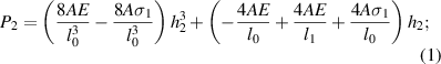

Figure 3. The elastic modulus measurement approach, numerical validation and experimental data. (a) Schematic of the straightening and stretching of a slack Pd nanoribbon. (b) Curve fitting of a typical  data of a Pd nanoribbon, with a varying fitting range (FR) and starting point (SP). (c) Validation of numerical fitting method using the simulated
  data from COMSOL. The distribution of calculated elastic modulus
  . (d) Histogram of calculated
  in the range of 50–200 GPa, with a mean value of 107.1 GPa. (e) The distribution of calculated elastic modulus
  of the experimentally measured
  data of a bare Pd nanoribbon. Pd thickness: 66 nm. (f) Corresponding histogram of measured
  to (e), with a mean value of 104.3 GPa. (g) The distribution of calculated elastic modulus
  of PdGr nanoribbon. (h) Corresponding histogram of
  to (g).
Download figure:
Standard image High-resolution imageNotably, due to the slack,  is greater than the real indentation-induced displacement of the Pd nanoribbon as shown in figure 3(a). In addition, there is a preload in nanoindentation for zero-deflection point detection. In this study, the preload is around 2 µN.
  can be expressed as the sum of the measured deflection data and slack height
  as well as the pre-deflection
  .
.


Based on this analysis, instead of the cubic-linear relation in the membrane model reported in previous studies [23, 25]. here we use a full 3rd order polynomial function (equation (4)) to analyze the  data:
data:

which gives precise and repeatable results of the elastic moduli taking into consideration the non-ideal initial slack geometry.
3. Results
The elastic modulus of the suspended nanoribbons can be determined by fitting the measured  loading or unloading curves using equation (4). However, the proposed load-displacement mathematical models accurately fit the measured data only in the range where the assumptions of the model hold: the nanoribbon which was originally slack became taut due to the indentation load. We observe that the uncertainty in zero-displacement significantly affects the fitting results since a small displacement drift can lead to large uncertainty in the elastic modulus due to the cubic term in equations (1) and (S4). For nanoindentation measurement on slack nanoribbons, we need to avoid the early stage in
  data (
 ) which corresponds to nanoribbon straightening deformation and fit the stretching dominated region which can be captured in the aforementioned analysis. Moreover, the nanoribbons can plastically deform at large strains in nanoindentation [16]. Fitting the full range of
  data using the elastic deformation models could hence lead to errors. To solve these limitations, a careful selection of the fitting range of raw
  data can be used to precisely determine the elastic modulus using the proposed indentation model, and this method is validated numerically.
Figure 3(b) illustrates the strategy to determine the elastic modulus of Pd thin films. The whole data is fitted using equation (4) (also equation (S6)) at various fitting ranges (FR) and varying starting points (SP), shown as the red dashed line in figure 3(b). Varying these two enables the determination of the taut configuration and extracts only the elastic modulus respectively. We calculate the root mean square error (RMSE) of the least square fitting to examine the goodness of curve fitting and use equation (S6) to determine the elastic modulus for Pd. It is important to first validate this fitting approach using finite element analysis (FEA) data. We model in COMSOL various nanoribbons having initial slack with different geometries and indent them to extract a numerical  curve, then apply the fitting approach to this data (see validation details in figures S2–S5 and SI). Figure 3(c) displays the calculated moduli using the proposed numerical fitting method on the simulated
  data (figure S3(a)) using equation (S6) with varying SPs and FRs. Figure 3(d) shows that the mean value of the curve fitted modulus corresponds to the modulus used in the FEA simulations (103 GPa) with less than 4% error. Figure S3(b) provides more insights into the variations in fitted modulus. It illustrates how very small SP leads to high RMSEs due to the slack. On the other hand, when the SP is too large, the nanoribbon is under initial tensile stress at the assumed zero-point which is not taken into account correctly. Moreover, if the fitting range is too large, plastic behavior at large ribbon deflections will affect the accuracy of the elastic model. As a result, the calculated moduli with small or large SP show unrealistic and inconsistent values from the given property (103 GPa) in FEA, as shown in figure 3(c). Notably, there is a fitting range with the intermediate SPs and FRs yielding consistent modulus and the minimum RMSE. Converting figure 3(c) into modulus histogram displayed in figure 3(d), we can determine the mean calculated modulus of 107.1 GPa, which has less than 4% error compared to the 103 GPa used as the input modulus in FEA. We have extensively validated the reliability of the proposed curve fitting method for the microbridge testing data analysis in SI. The proposed analysis method is robust for the different slack geometry (with a 'S' shape, see figure S4), as well as the nonsymmetric loading case (see figure S5).
This approach is used to measure the moduli of Pd and PdGr nanoribbons from indentation of suspended microbridges such as the ones shown in figures 1 and 2. Figures 3(e) and (f) display the curve fitting results with the measured  data of a slack Pd nanoribbon in the microbridge testing. The mean values and the data distributions are shown in figures 3(f) and (h), and the moduli of Pd and PdGr are found to be 104.3 GPa (66 nm thick) and 142.5 GPa (71 nm thick) respectively. Similarly, we gain more insights by inspecting the roles of SP and FR on the measured mean modulus. Figures 3(e) and (g) show the existence of a fitting range in which the calculated elastic modulus is stable relative to variations in SP or FR, while also maintaining low RMSE (figure S6(a)). A small SP or FR, e.g. FR = 1.8 µm, leads to high RMSE and fluctuating modulus, which indicates poor goodness of fitting due to the geometry of slack and deformation in Pd nanoribbon at the beginning of nanoindentation. While a large SP or FR, e.g. FR = 2.2 µm, gives the decaying modulus as SP increases due to plasticity effects taking place at large deflections. Notably, there is a plateau in
  that is independent of SP and FR and reflects the real elastic property of the nanoribbon, see the zoomed-in inset in figure S6(b). This plateau in
  coincides with the mean modulus value of 104.3 GPa shown in figure 3(f). For the
  region where the elastic theoretical model applies, consistent
  and low RMSE are expected. Figure S6(c) presents the correlation of calculated
  and RMSE.
The indentation of graphene-coated Pd (PdGr) shows a significant increase in the measured modulus compared to Pd. Figures 3(g) and (h) display the  distribution in the fitting space and the corresponding
  histogram for one indentation data for a PdGr nanoribbon. Figure S7 also displays the corresponding RMSE and
  distributions for cyclic loading, from which we can determine the mean
  value at
  for a 71 nm thick PdGr film. Notably, there is about 47 nm deviation in the measured width of as-grown PdGr nanoribbon (figure 1(e)), which may affect the modulus calculation. Figure S8 compares the modulus histograms considering the PdGr width non-uniformity, and shows < 2.3% error in mean
  value. Compared to as-deposited Pd nanoribbons, there is over 35% increase of
  due to bilayer graphene
  on the surface. Graphene is expected to have strong interfacial adhesion on Pd so we assume that there is no interfacial slip within the elastic regime [34]. The results can also be affected by changes in the Pd during synthesis [17] where carbon diffuses into interstitial sites and could alter the elastic properties of the nanoribbon. We hence isolate the graphene reinforcement effect by removing the graphene layers from the same PdGr sample with RIE and testing the nanoribbon (also named as PdC to indicate that the Pd contains carbon). The elastic modulus of a 71 nm thick PdC film is measured by indentation and is found to be
  . This confirms that the significant increase in PdGr can be partially attributed to the changes during CVD leading to the PdC in Pd (see later discussion on carbide-like PdC). This approach allows us to precisely study the contribution of as-grown bilayer graphene to the composite elasticity while examining the role interfacial mechanics on the elastic behavior of the nanoribbons.
4. Discussions
4.1. The role of graphene and its interfacial mechanics in the elastic behavior of PdGr composite
The material system selected for this study has strong advantages for mechanical load transfer. It is known that Pd strongly interacts with graphene as also manifested by the small separation between the Pd and C atoms (0.23–0.25 nm on Pd (111) surface), a value smaller than the interlayer separation in graphite and smaller than the separation between graphene and other transition metals [34, 35]. The interfacial mechanics is governed by in-plane strain mismatch between graphene and Pd (111) for instance is ~3.3% in compression [31]. The sputtered Pd thin films after annealing are predominantly (111), see electron backscattering diffraction (EBSD) analyses in figure S9. Moreover, due to mismatch between the thermal expansion coefficients of graphene and the seed metal, graphene is usually in strain after synthesis.

Figure 4. Raman spectroscopy in a freestanding PdGr thin film. (a) Raman spectra of freestanding PdGr nanoribbon and clamped PdGr on SiO2. The G peak in freestanding region is subjected to red shift with respect to that in supported region, representing the tension in graphene on freestanding Pd. Inset SEM image shows the corresponding freestanding and supported region on a PdGr nanoribbon. Scale bar: 2 µm. (b) Correlation of frequencies of G and 2D Raman modes in freestanding PdGr and supported PdGr nanoribbons. Frequency data is collected from Raman maps taken with laser excitation wavelength of 532 nm and exposure time of 15 s. The unstrained and undoped Gr (transferred onto a SiO2/Si substrate) has the average  at 1607 cm−1 and
  at 2696 cm−1. The blue doping line is extracted from reference, assuming
  [37].
[37].
Download figure:
Standard image High-resolution imageThe interfacial strain in as-grown PdGr nanoribbons can be characterized using Raman spectroscopy because it affects the orbital hybridization of the carbon atoms hence it shifts the G and 2D peak frequencies. Figure 4(a) shows the Raman spectroscopy of PdGr nanoribbons clamped on a TEM grid and used for indentation. We observe two types of Raman spectra. Firstly, on the clamped region where the PdGr is supported on SiO2/Si TEM grid, Raman spectroscopy shows single sharp G peak at ~1606.3 cm−1 and 2D peak at ~2695.4 cm−1. Whereas, there is an obvious red shift in G mode frequency to ~1551.6 cm−1 for the freestanding region on the same Pd nanoribbon. It is known that this Raman shift is due to not only the strain in graphene but also the doping effect from metallic substrates [36, 37]. We can extract the strain effect in graphene by isolating the Pd substrate effect from Raman frequencies correlation, as shown in figure 4(b). There is an offset in the correlation of Raman  frequencies between the pristine graphene (with no strain no doping) and as-grown graphene on the Pd substrate. It has been investigated that graphene supported on strongly interacting substrates, e.g. Ni and Pd [34, 35], can be doped and show blue shifts in Raman frequencies compared to the pristine graphene [37]. The purple line in figure 4(b) represents the
  correlation of graphene with different doping levels but in the same strain state. As a result, graphene grown on the supported Pd area is slightly compressed. This can be attributed to the lattice mismatch strain (
 ) between graphene and Pd, as well as the polycrystalline substrate texture [30]. Notably, there is obvious red shift in
  correlation of graphene grown on the freestanding region of a PdGr nanoribbon, indicating that graphene is stretched in these region [36]. The apparent slope in figure 4(b) is the strain slope, where the data points at the bottom left corner are under the largest tensile mismatch strains. This agrees with the straightening of the nanoribbons and the associated decrease in slack observed in the 3D profile measurements. The exact absolute value of the strain cannot be precisely determined from these measurements since it requires calibration to the Raman spectrum of graphene sitting epitaxially on Pd but without any mismatch strain. We use the results of figure 4 to qualitatively demonstrate the tensile strains in the graphene in the suspended nanoribbons.
4.2. Thickness-dependent elasticity of PdGr composite
Using these insights, we analyze the contributions of the graphene and the interfacial mismatch strains on the measured moduli of PdGr. We adopt a new 3D/2D rule of mixture approach that treats the PdC as a 3D 'bulk' material, while treating the graphene as a 2D 'surface'. The advantage of this approach is it allows us to use the reported properties of 2D modulus of graphene and other nanomaterials without assumptions on the graphene thickness. The number of layers of graphene can simply be incorporated in the model. Further, the critical role playes by the nonlinear modulus component of the graphene (softening) is considered especially given the existence of strain mismatch between the graphene and the nanoribbon. The tension per unit width in the deflected nanoribbons is
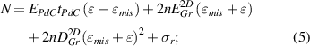
where  is the tensile force per unit width during indentation,
  is the nanoribbon thickness,
  is the number of graphene layers (for example
  for bilayer graphene), here we ignore the interlayer sliding in few-layer graphene and assume each layer effectively interacts with the underlying Pd substrate. This is a suitable assumption due to the small strains applied.
  is the uniaxial tensile strain in PdGr composite nanoribbon during nanoindentation,
  is the residual stress in the nanoribbon due to stretching over the trench during growth, and the factor 2 in equation (5) accounts for the top and bottom surfaces of the nanoribbon. Here, we ignore the thickness of graphene layer and introduce the 2D elastic constants
  . Since molecular dynamic simulations and experiments suggest that graphene shows quadratic dependence on strain [13, 38], we consider the nonlinear elastic behavior of as-grown graphene layer on Pd nanoribbons with a third-order elastic constant
  . The nonlinear elastic constitutive behavior of graphene can be expressed as
  [13]. We define the volume fraction
  . Straining of the Pd surface by graphene synthesis could introduce the surface stress, which can contribute to the measured modulus when the nanoribbon is strained due to the quadratic term.
In this study, we use very small nanoindentation strains so that  . As a result, we can expand equation (5) and ignore the resulting
  term, giving:
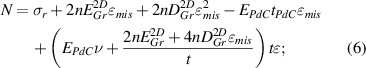
where the interfacial strain due to growth cancels out  . The term in the bracket of equation (6)
  is then equivalent to the measured elastic modulus of PdGr composite nanoribbon as it depends on the applied indentation strain
  . Therefore,
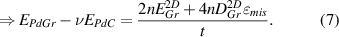
A couple of insightful conclusions can be drawn from this simple analysis: (i) the quadratic modulus of graphene leads to the dependence of the measured modulus on the mismatch strain  ; and (ii) the term
  can be a directly measured and used to analyze the relative contributions of the graphene modulus
  and the mismatch strain
  on the nanoribbon elastic response. Figure 5(a) shows the measured moduli of Pd, PdGr and PdC with different film thicknesses. Indeed, experimentally, the elastic modulus of bare Pd does not vary within the thickness range from 36 to 300 nm in this study. On the other hand, as discussed before, the elastic modulus of PdGr thin films significantly increases after the synthesis of graphene, and this increase is scale dependent. More specifically, the PdGr modulus increases notably as film thickness reduces. This not only stems from the contribution of high in-plane stiffness of graphene in PdGr composite, but is also affected by the graphene nonlinear elastic term
  and the large Pd-graphene interfacial stress. Notably, after etching the graphene layer away, we also release the interfacial elastic energy installed between graphene and Pd. This confirms the nontrivial contribution of the Pd-graphene interfacial stress on the elastic property in PdGr composites.

Figure 5. Increase in elastic modulus of graphene-coated Pd. (a) Dependence of the elastic moduli of bare Pd, PdGr and PdC on thin film thickness. (b) Dependence of  on thin film thickness. Dashed line represents the fitted curve in the form of
  .
.
Download figure:
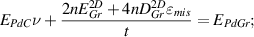
Standard image High-resolution imageFigure 5(b) plots the equation (7) with the measured  and
and  . By the least square fitting,
  . This suggests that graphene-induced surface strain from high temperature synthesis can significantly modify thin film materials' elastic modulus. Using the values from [13, 38] and
  for bilayer graphene, we find a mismatch strain
  (tensile). More generally, it shows that graphene is an effective reinforcement in Pd up to volume fraction of ~0.3%.
Next, we try to study the origin of increase of the PdC modulus ( ) by 14.8% compared to that of Pd (
 ) even when the graphene is removed by etching. Besides the expected interstitial carbon reinforcement effect, we also investigated the formation of palladium carbide-like phase close to the Pd surface after graphene growth. Figure 6(a) shows a cross sectional TEM image of a PdGr thin film which shows the graphene layers as well as the fringes associated with the atomic spacings of the Pd. We measured the Pd lattice fringes near the Pd-graphene interface and noted that they are expanded to about 7.2% in comparison with Pd bulk values (figure S10). This expansion can be related to carbon incorporation into the Pd lattice especially in the sub-surface sites [39]. Importantly, carbon atoms in this carbon-rich layer close to the Pd surface have preferred interstitial sites and can form a carbide like Pd-C phase [40–42]. The formation process of this Pd-C phase is unclear, nevertheless, there is a number of theoretically reported stable Pd-C phases exhibiting very high stiffness and hardness [43]. In light of these considerations, it is reasonable to propose a model with Pd/Pd-C/Gr laminated structure for the grown PdGr composite thin film, as shown in figure 6(b). In order to confirm the existence of Pd-C layer in Pd subsurface, x-ray photoelectron spectroscopy (XPS) is used to track the core level shift in Pd peaks. XPS measurements are made using a Kratos Axis Ultra x-ray photoelectron spectrometer using monochromatic Al Kα radiation (1486.6 eV). The x-ray detection depth is about 10 nm. The binding energies are referenced to the graphitic C 1s signal at 284.4 eV. We tilt the PdGr surface so that more subsurface signal could be collected. Figures 6(c) and (d) present the Pd 3d and C 1s XP spectra of as-grown PdGr thin film. As expected, the carbonaceous species shift the binding energy (BE) of surface Pd atoms to the high BE side of the bulk Pd signal (core level of Pd 3d5/2~335.1 eV). The BE for this carbon-rich species is found at about 335.7 eV, which is 0.6–0.8 eV shifted from Pd 3d core level. This agrees well with the experimental and calculated results for the sub-Pd surface Pd-C phase [40, 41]. In figure 6(d), the C 1s peak at BE = 284.4 eV is assigned to graphene related peaks. The peak asymmetry toward lower BE with a low intensity peak at ~283.7 eV is a signature of the presence of carbide, which can be related to Pd-C bonds.

Figure 6. Formation of palladium carbide at the Pd-graphene interface during CVD synthesis. (a) TEM image shows the cross section of a PdGr nanoribbon. Pd lattice expands close to the Pd-graphene interface. Scale bar: 2 nm. (b) Schematic of Pd-PdC-Gr laminated composite structure in PdGr thin films. Notably, strong interfacial stress between Pd-graphene layers contribute to the elastic properties of PdGr nanocomposites. (c) Pd 3d5/2 XP spectra for the grown PdGr thin film using 1486 eV excitation energy. The Pd component at 335.1 eV corresponds to bulk, metallic Pd, whereas the higher binding-energy peak (335.7 eV) represents the core-level shift components including palladium carbide. By tilting the sample to the angle w.r.t. beam, the Pd surface properties can be amplified. With 15° tilting angle, higher binding-energy peak (335.9 eV) associated to PdC is observed. (d) C 1s XP spectrum for the grown PdGr thin film. A sharp peak at 284.4 eV confirms the sp2 hybridized carbon (graphene), while a tiny lower binding-energy indicates the existence of carbide.
Download figure:
Standard image High-resolution image
With the presence of the carbide phase near the Pd-graphene interface, we can separate the 3D elastic modulus of PdC into the carbide boundary layer modulus  and the pure Pd modulus
  with the rule of mixture as
  , where the surface layer thickness is
  and the volume fraction
  . The thickness of
  can be estimated from the fringe spacings in the TEM of figures S6 and S7. For example, for PdGr-4,
  and
and  , with the measured
  . Using the measured value of
  , we can estimate the modulus for carbide phase about
  , which is in the range of the reported theoretical results [43]. It is possible that multiple types of stable carbide phases coexist in PdGr thin film. However, this simple analysis leverages the imaging and XPS to rationalize the measured increase in modulus of the nanoribbons even when the graphene layer is etched.
5. Conclusions
In summary, we study the behavior of Pd nanoribbon coated with graphene by CVD. We observe that the presence of bilayer graphene significantly increases the nanoribbons' elastic modulus, and the increase can be mathematically modeled using a framework that considers the graphene's contribution to the material's surface modulus. This enhancement not only stems from the high in-plane modulus in graphene layer, but is also affected by its nonlinear elasticity which plays a critical role owing to the interfacial stress induced by the lattice mismatch during CVD synthesis. Notably, the interfacial stresses at the graphene-metal interface is reminiscent of the role of interphase in polymer nanocomposites [44]. With good load transfer, graphene can be a very effective reinforcement filler in metal-matrix composites, and the level of reinforcement is strongly dependent on the stresses at the interface. In addition, a very stiff Pd-C carbide-like phase is observed near at the interface after graphene growth. This study suggests a new route to enhance and study the elastic behavior of nanoribbons and thin films for applications ranging from flexible electronic devices to chemical catalysis.
Beyond the engineering applications of this material, this study employs several innovative aspects to reach its conclusions: (i) the selected material system—namely PdGr—offers the critical advantage of strong interfacial interaction and hence achieves effective strengthening; (ii) the method of microbridge indentation is refined to account for the uncertainties in the measured modulus due to the non-ideal bridge geometry; (iii) the composite modulus is compared to and agrees with a rule of mixture mathematical model which considers the effect of graphene as a 'surface' modulus added to the 'bulk' modulus of Pd; (iv) the nonlinear modulus of graphene, which plays a critical role when interfacial residual stresses are present, is calculated, and finally (v) the role of Pd carbide, which forms during the graphene synthesis, is considered.
Acknowledgement
K Z, M S and S T acknowledge support from the Office of Naval Research ONR N00014-18-1-2457 and from the NSF 1825300. The authors acknowledge helpful discussion with Professor Harley Johnson and Dr Pascal Pochet.