

Abstract
Single-point diamond turning assisted with slow/fast tool servo is a viable technique for complex microlens arrays manufacturing. However, there are still challenges one must overcome when efficiently fabricating microlens arrays with discontinuous features. In this study, a novel slow-tool-servo diamond turning method, termed toroid-surface-based slow tool servo turning method, was proposed for generation of discontinuously structured microlens arrays. A discussion on the advantages for processing discontinuous features was presented and a hexagonal spherical microlens array over a large area was fabricated using the proposed method. This toolpath generation strategy, combined with a segmented turning approach, was adopted with consideration of both the geometry of the diamond tool and the profile of the microlens array. The surface roughness, form accuracy and geometry periodicity, were investigated. Results indicated that the entire microlens array has high homogeneous quality for optical elements. The fabricated microlens array was further utilized as a mold insert in a precision chalcogenide glass molding process. Compared with conventional fabrication methods, this novel technique method can be successfully implemented to fabricate various discontinuous microlens arrays with high accuracy and great efficiency.
Export citation and abstract BibTeX RIS
1. Introduction
Due to their superior performance for both visible and infrared optical applications, microlens array based optical systems are used extensively for both imaging and non-imaging optical designs [1–6]. To satisfy the performance requirements for microlens arrays, several fabrication techniques have been proposed [1–3, 7–9], most of which can be classified into mechanical and chemical processes. Compared with mechanical processes, chemical and physical processes are restricted by a limited selection of materials and few surface geometries. On the other hand, machining, a mechanical process, is more universal and flexible for the generation of microlens arrays [3], especially for intricate surface profiles. Among these techniques, single-point diamond turning with slow and fast tool servo (S/FTS) are some of the most popular approaches in micro-optics fabrication on a variety of engineering materials with intricate geometry [10, 11].
Single-point diamond turning assisted with slow/fast tool servo is a robust technique for manufacturing of micro-optics with flexibility and high-efficiency [3, 12]. Synchronization of the translational and rotational movements of a machine tools' slides and spindle enable S/FTS diamond turning to fabricate intricate freeform surfaces [11, 13]. Typically, FTS diamond turning is best suited for the generation of small-amplitude microstructures on plane/curved surfaces with piezoelectric-driven add-ons, whereas STS is better suited for small curvature, low frequency surfaces. For example, hierarchical three-dimensional (3D) artificial compound eyes on curved surfaces have been efficiently fabricated with the assistance of an FTS [10, 14].
In previous papers, we have successfully fabricated micro-optics with intricate surface geometries on aluminum molds by means of S/FTS diamond turning [10, 11]. However, due to the lack of full consideration of the curvature change in the tool path, deviations from the original optical design may result when machining discontinuous optical features. Issues contributing to this problem can be summarized as follows,
- (I)Bandwidth limitation. Microlens arrays are usually uniformly distributed in the Cartesian coordinate system. When transformed to the cylindrical coordinate system for machining, the diamond tool needs to pass through a higher number of lenslets at larger radii, requiring higher tracking bandwidth for the machine tool servos. Consequently, this also restricts the spindle speed during the turning process. Additionally, the high inertia of the mechanical slides can lead to dynamical errors in the machined optic, fundamentally caused by the higher frequency of the optical surface. Lastly, since fewer lenslets are located at smaller radii on the surface, the cutting operation will not remain at a constant speed, which can induce noises into phase and position control [15, 16].
- (II)Tool compensation on discontinuous features. The lenslet boundaries on the optical surface are usually sharp and derivative discontinuous. This makes STS diamond turning very difficult to fabricate perfect geometry at the edge because of discontinuity of surface derivative in this transition area [17]. In tool nose radius compensation, the discontinuity in surface derivatives results in sharp change in the direction of the tool path. The lenslet aperture, where the sudden tool path change occurs, may be poorly formed as the tool passes over it, leaving scratches on the edges around each lenslet. By purposely selecting a lower feedrate and smaller tool nose radius, machining defects can be minimized at the expense of efficiency.
These defects can significantly deteriorate the quality of machined micro-optics. In this paper, a novel machining method, toroid-surface-based turning method, is proposed to improve the machining accuracy and efficiency of microlens arrays. First, the method is presented in theory. After combining with a segmented turning method, a hexagonal microlens array is fabricated on an aluminum 6061 mold with novel STS diamond turning method. Then, the surface roughness, form accuracy and geometry periodicity are measured. Lastly, an infrared microlens array is molded by a precision glass molding process. The uniformity and surface quality of the molded microlens array demonstrates the feasibility of the proposed fabrication process.
2. Principle of toroid-surface-based turning
In the toroid-surface-based turning process, the X and Z-direction translation of the tool is synchronized with the C-axis rotational motion of the workpiece to enhance the machining accuracy and efficiency [18]. Figure 1(a) illustrates an ultraprecision diamond turning lathe with the STS process. The diamond turning lathe pictured consists of three-axis linear axes (X, Y and Z) and two rotational axes (B and C). In STS diamond turning, the Y-axis and B-axis motions are fixed after initial tool setting. Typically, the diamond tool is fixed on the tool post and the workpiece is mounted to the main spindle via a vacuum chuck. By transforming an optical design in the Cartesian coordinate system to a machine tools' cylindrical coordinate system, a microlens array can be conveniently fabricated by synchronizing its linear (X, Z) and rotational (C) motions.
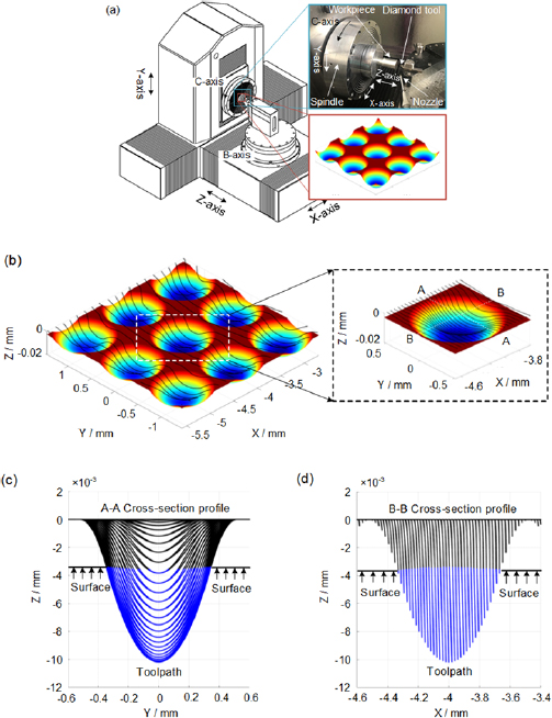
Figure 1. Schematics diagram of (a) ultraprecision diamond turning configuration with STS, (b) toolpath generation strategy for discontinuously featured microlens array, (c) A–A cross-section profile and (d) B–B cross-section profile for toolpath.
Download figure:
Standard image High-resolution imageThe principle of toolpath generation for a single circular lenslet is shown in figure 1(b). To avoid sharp changes in the direction of the toolpath (discontinuous derivative), a transition zone is added around each lenslet. In the current design, this transition zone is a small portion of a toroid surface. Per this design, the diamond tool traverses through air along the toroid portion of the toolpath and cuts material along the lenslet portion of the toolpath. The section profiles along A–A and B–B illustrate the continuous toolpath along the cutting and feed directions in a single turning cycle, as shown in figures 1(c) and (d). In this fashion, the sharp change in the direction of the toolpath can be totally avoided, which improves the motion accuracy by minimizing dynamic errors of the linear slides. By repeating the basic process, a microlens array can be precisely generated, covering the entire surface with arbitrary apertures.
The advantages for processing microlens arrays with discontinuous features can be summarized as follows: (a) the diamond tool maintains a steady motion when driven at constant speed along the smooth toolpath. This improves the accuracy of motion by reducing excessive machine tool accelerations. Consequently, lenslet profiles are precisely machined; (b) the distance between the plano surface and toolpath keeps the diamond tools away from the plano surface, avoiding deterioration of the machined surfaces due to dynamic and thermal disturbances from the surroundings; and (c) the smooth toolpath makes the best of linear motions, resulting in near-constant optimal cutting speed and rotary speed of the main spindle.
3. Generation of segmented turning tool path
To investigate the feasibility of this method in diamond turning, a hexagonal microlens arrays, with discontinuous apertures, are adopted in the continuous diamond turning process. Considering toroid surface and tool nose compensation, the optimal toolpath generation strategy is described in detail as follows.
3.1. Toolpath generation for each lenslet
In toroid-surface-based turning, the toolpath geometry consists of two separate parts: the toroid surface transition and the designed lenslet profile. In the example shown in figure 2, a torus with constant minor/major radii is shown. For freeform/aspherical lenslets, a torus with variable major/minor radii can be used to connect close features with smooth curves. The toroid surface can be described in its local Cartesian coordinate system ow − xwy wzw about the z-axis by:

where c is the major radius, from the center of the hole to the center of the toroid cross section, and r is the minor radius of the toroid cross section.
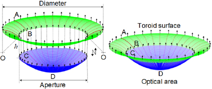
Figure 2. Toolpath generation method for basic turning cell, consisting of optical area and transition area.
Download figure:
Standard image High-resolution imageSince the profile consists of two separate surfaces, stitching toroid surface and the spherical/aspherical surface together is critical. Assume that a toroid surface with minor radius r is used and the three-dimensional (3D) geometry is simplified into a two-dimensional (2D) profile on the cross-section plane. To stitch these two sections A-B and C-D together, connect the joints B and C with the same gradient and distance from the center axis. First, determine the points with the same gradient. The derivatives of the toroid surface in Cartesian coordinates is expressed by:
The normal vector of the lens profile at the edge point C (xC, y C, zC) can be expressed as  . Points B (xB, y B, zB) with equal gradients
  on the toroid surface can be determined by adjusting the coefficient c in the equation for the points on the edge between two surfaces. When the parameters r and c are identified, the gap between the edges of the optical area and the toroid surface h can be adjusted to zero by moving the position in z direction.
The entire microlens array can be machined by repeating the cutting process for each lenslet consisting of a toroid surface and a lens profile.
3.2. Segment diamond turning toolpath generation
Due to the toroid surface transition around each lenslet, some complicated connected features fail to be generated in one single operation. One such example is a hexagonal microlens array, which consists of sharp edges among neighboring lenslets due to its high fill factor. In order to generate such optical features, a segmented diamond turning method was adopted [18], as shown in figure 3(a). In the present experiment, the entire microlens array is divided into four groups, which are processed sequentially in four steps. The lenslets in each group are located such that a toroidal blend will fit between adjacent lenslets, as shown in figure 3(b). The dashed circles around each lenslet illustrate the basic cells with toroid surface, which connects the flat surface and lens geometry and has continuous 1st derivatives. The gaps between adjacent lenslets in the microlens array are determined by the profile of the toroid surface.
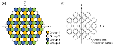
Figure 3. Toolpath generation for segment diamond turning (a) classification into four groups, and (b) basic turning cells for group 1.
Download figure:
Standard image High-resolution image4. Experiment setup
Diamond turning experiments were conducted on an ultraprecision CNC lathe (350FG, Moore Nanotechnology, Inc., Keene, New Hampshire, USA) with five-axes. The single-crystal diamond tool with a 2.54 mm tool nose radius (K&Y Diamond, Ltd, Diab St-Laurent, Quebec, CA) was fixed on the tool post, which could follow the transitional servo motion along the Z-axis, while the workpiece, an aluminum alloy 6061 mold, was clamped on the air-bearing main spindle by vacuum. The optical surface interferometer (Wyko NT9100, Bruckner, Tucson, Arizona, USA) was used to evaluate the surface geometry after diamond turning. Subsequently, a precision glass molding process was carried out on a commercial PLC molding machine Model GP-10000HT (Dyna Technologies, Inc., Sanford, Florida, USA). Details of diamond turning parameters are shown in table 1.
Table 1. Diamond turning parameters.
| Material | 6061 aluminum alloy |
|---|---|
| Spindle speed S | 15 rpm |
| Feedrate f x | 2 μm/rev |
| Tool nose radius Rt | 2.54 mm |
| Tool rake angle γ0 | 0° |
| Tool clearance angle α0 | 7° |
| Workpiece dimension | D 25.4 mm × H 52 mm |
The mathematical description for each lenslet can be expressed by Zernike polynomials, which include a regular conic aspheric surface and extended polynomial terms, as follows [13]
where z is the sag of the surface and  , c and k are the conic constant and vertex curvature, N is the number of Zernike polynomial terms, and Ai is the magnitude coefficient of the ith extended polynomial term. Relevant microlens array parameters are shown in table 2.
Table 2. Parameters for the hexagonal microlens array.
| Conic constant c | 1 |
|---|---|
| Radius, r | 8.845 mm |
| Height of each lenslet, h | 6.676 μm |
| Pitch, p | 0.6 mm |
| Aperture, a | 0.6928 mm |
| Minor radius, r | 4.4225 mm |
The hexagonally distributed microlens array design is shown in figure 4(a). The corresponding toolpath, generated by the strategy described in section 2 by offsetting the tool in the direction of the normal vector, is illustrated in figure 4(b).
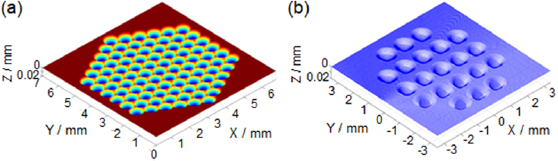
Figure 4. Schematic diagram of (a) the microlens array design and (b) corresponding optimal toolpath for group 1 lenslets.
Download figure:
Standard image High-resolution imageFor demonstration purposes, in figure 4(b), the radial stepover is intentionally increased to 20 μm/rev to show a clear view of the STS toolpath for lenslets in group 1. Also, in figure 4, it is clear that the designed microlens array itself is discontinuous, whereas the toolpath is globally continuous due to the presence of the toroidal blend.
The machined microlens array mold is further employed in a precision glass molding process. The entire precision glass molding process is shown in figures 5(a)–(d). A small, polished chalcogenide glass (As2Se3) disk is placed between the molds. After three purging cycles with nitrogen gas, the mold temperature is heated to 215 °C and held constant at this level for 15 min. The upper mold is then pressed onto the chalcogenide glass disk with 150 N load. To ensure the microlens cavities are completely filled, the upper mold is continuously loaded until its position remains unchanged for ~5 min [19]. Once the cavities are filled completely, an external fan is turned on and the temperature of the mold is dropped to ~40 °C. Lastly, the vacuum chamber is unlocked and the molded microlens array is removed from the bottom insert. Relevant precision glass molding parameters are shown in table 3.
Table 3. Parameters for precision As2Se3 glass molding.
| Molding material | As2Se3 |
|---|---|
| Heating rate, Ch | 5 °C s−1 |
| Molding temperature, Tm | 215 °C |
| Molding load, F | 150 N |
| Holding time, Th | 15 min |
| Cooling rate, Cc | 0.5 °C s−1 |
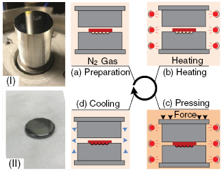
Figure 5. Schematic diagram of precision As2Se3 glass molding cycle, (a) N2 purging, (b) heating, (c) pressing & temperature holding, and (d) demolding.
Download figure:
Standard image High-resolution image5. Result and discussion
5.1. Characteristics of the machined structures
The feasibility of the toroidal-surface based turning was demonstrated by generating a hexagonal microlens array on a 6061 aluminum alloy mold. Figure 6 shows the photograph of the machined Al mold and micro-structures on the machined surface. An arbitrary region of the microlens array is obtained with an amplification 2.5 × and shown in figure 6(b). From the photograph, each lenslet clearly shares the same hexagonal profile without visible distortion or scratches on their boundaries. The clean and sharp edge around each lenslet suggests that the proposed toroidal-surface turning process is an effective and robust method in discontinuous feature fabrication.
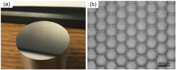
Figure 6. (a) Machined aluminum mold, and (b) microlens array on machined surface.
Download figure:
Standard image High-resolution imageTo evaluate the form accuracy of the microlens array, the micro-structures of the microlens array are further captured and stitched by the optical profiler using a 5 × objective lens, shown in figure 7. The homogeneity in the measured lenslets in figures 7(a) and (b) indicates good uniformity by the proposed STS turning approach. The 2D surface profile in figure 7(c) (profile along A–A in figure 7(a)) further illustrates that the finished form of the lenslets agree well with each other. The depth deviations between each lenslets are within 15 nm. The observed distance between two successive lenslets is about 601 μm, which agrees with the design values in table 2. More importantly, figures 7(b) and (d) show cross-section profiles passing through the centers of the lenslets along three-directions, A–A, B–B and C–C. These cross sections match well with each other, showing no obvious distortion for each lenslet. The height of the lenslet is 5.22 μm with 601 μm diameter aperture, and the distance between two successive lenslets is about 601.4 μm along A–A, which are in good agreement with the design.
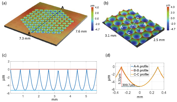
Figure 7. Characteristics of the generated hexagonal microlens array, (a) 3D micro-topography of the whole area, (b) an arbitrary region of the microlens array, (c) 2D cross-section profile along A–A, and (d) 2D profile along three directions through lenslet center.
Download figure:
Standard image High-resolution imageThe surface quality is further analyzed by selecting one arbitrary lenslet from the microlens array, as shown in figure 8(a). Cross-sectional profiles of this lenslet are obtained along two directions passing through its vertex, as shown in figures 8(b) and (c). Compared with design, the obtained profile has a good agreement with the desired profile and the corresponding error is less than 70 nm. After removing the spherical form of the lenslet from the obtained surface geometry, figure 8(d) shows the surface details after the STS turning process. The surface roughness (Ra) of the machined surface is 13.65 nm. In the feed direction, the fluctuation in depth is likely due to the tool residual marks. In the cutting direction, very tiny fluctuation is observed, indicating that the proposed method largely restrained vibration in the STS diamond turning process.
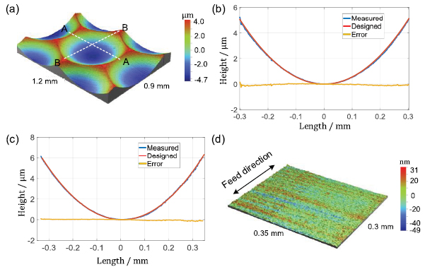
Figure 8. Micro-structures of one lenslet (a) 3D micro-topography of the lenslet, (b) 2D cross-section profile along A–A, (c) 2D cross-section profile along B–B, and (d) surface micro-topography after removing substrate profile.
Download figure:
Standard image High-resolution image5.2. Characteristics of the molded surface quality
Further measurements were conducted after precision glass molding to characterize the finish surface quality and uniformity. Similar with the profile measurement after mold fabrication, 3D and 2D profiles are obtained using an optical surface profiler. The micro-photo of the molded microlens array shows good uniformity, as shown in figure 9(a). The whole 3D micro-structure of the molded microlens array is captured and stitched, shown in figure 9(b). This illustrates the homogeneous surface geometry and quality over the whole area. The cross-section profiles along A–A in figure 9(b) is shown in figure 9(c), which illustrates the depth of lenslets are the same and sharp ridges along each lenslet are well molded. In addition, the cross-sectional profile along each lenslet was also measured, as shown in figure 9(d). The profiles along two perpendicular directions showed good agreement with the design profile and the profile deviation is limited within 60 nm. The measurement results show that the geometry of the mold has been successfully transferred to the chalcogenide glass with high fidelity. Finally, the surface micro-topography is measured by using a microscope using a 100 × objective. The surface roughness (Ra) is 15.61 nm, which matches that of the mold surface.
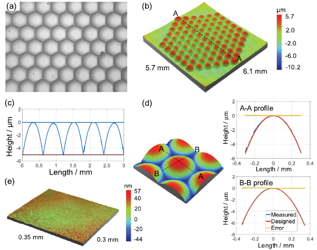
Figure 9. Micro-structures of the molded microlens array (a) micro-photo of the microlens array, (b) 3D micro-structure of the whole microlens array and (c) 2D cross-section profile along A–A, (d) micro-structure of one lenslet and cross-section profiles, and (e) surface micro-topography after removing profile.
Download figure:
Standard image High-resolution image5.3. Optical performance of IR optics
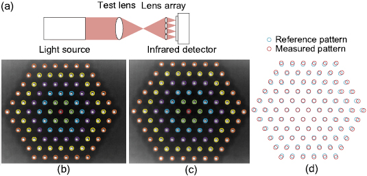
The microlens array is originally designed for an infrared (IR) detector to form a Shack–Hartmann sensor. The imaging quality of the microlens array is tested by a self-made optical system [20], as shown in figure 10(a). The IR light source employed in this experiment is a multiple wavelength coil-wound heating element (HawkEye Technologies, Infrared Source IR-35, Milford, Connecticut). A spherical Germanium (Ge) lens (Thorlabs Inc., Newton, NJ, USA) is mounted next to the IR light source to generate a spherical wave. The molded microlens array is located on a three-axis (3D) microstage. In this setup, both the distance between the microlens arrays and the IR detector can be precisely adjusted to the focal length of the lenslets. The up-and-down motion of the platform can also provide flexibility for centering the image. The raw data frame captured by the IR detector is shown in figures 10(b) and (c). The uniformly located bright circle imaging results demonstrate good optical performance of the molded infrared microlens array.
Figure 10. (a) Schematic of the optical setup, and (b) reference image, and (c) measurement image from the infrared detector with recognized light spots and (d) relative position between the reference and measured pattern.
Download figure:
Standard image High-resolution image
6. Conclusion
A novel STS assisted diamond turning method was proposed and demonstrated for large-area microlens array fabrication. To demonstrate its utility, a hexagonal microlens array for IR microlens array replication was machined.
Toolpath generation strategy and stitching approach were introduced to reduce machine tool accelerations in high fill factor, globally discontinuous microlens array. By using a toroidal surface, discontinuous toolpaths can be avoided. Further analysis is conducted to analyze the dynamical vibration in diamond turning.
Based on the discontinuous features between the adjacent microlenses, a hexagonal microlens array is divided into four separate zones, each of which is regarded as one basic fabrication unit. The turning process is completed in four consecutive steps.
Finally, a large-area hexagonally distributed microlens array is fabricated and subsequently utilized in a precision glass molding process. The globally homogeneous surface quality and optical performance of the molded microlens array demonstrates a promising process for further applications in optical engineering.
Acknowledgment
This work was also supported in part by the II–VI Foundation block-gift program. This work was partially supported by the National Science Foundation (NSF) (Grant No. 1263236). Opinions, findings, and conclusions or recommendations expressed in this material are those of the authors and do not necessarily reflect the views of the National Science Foundation. The authors acknowledge the generous support from Professional Instrument for the ISO 2.25 spindle used for high speed milling operation in this research.
Funding information
National Science Foundation (NSF) (1537212); Ohio State University (OSU).