

Abstract
This paper presents a simple design of gold MEMS, with a central test specimen undergoing tensile loading, for the experimental characterization of elastic–plastic behavior using electrostatic actuation. A kinematic model for the test microstructures is presented that relates the experimentally measured deflection in the test specimen to the developed axial and bending stress. Moreover, an elastic–plastic beam bending model is presented to analyze the development of plastic hinges in the central test specimen. The design of test microstructures allows us to achieve stress values higher than the yield stress of the gold specimen before the pull-in effect, thus allowing to analyze the effect of elastic–plastic behavior on the static deflection profile of the central test specimen under repeated loading. The actuation voltage-deflection tests under repeated loading, both in the elastic and elastic–plastic region, allowed to estimate the applied stress limit for the onset of plasticity in gold thin film based MEMS devices.
Export citation and abstract BibTeX RIS
1. Introduction
The accurate characterization of the mechanical properties of the structural materials in the MEMS devices like Young's modulus, yield strength, fracture strength, creep, residual stress and stress–strain relationship under varying loading conditions have been of major concern for the MEMS device design and reliability. The operation of a MEMS device is strongly affected by the uncertainty in both the electrical and mechanical properties of the materials. This uncertainty is generally related to the microfabrication process, structural parameters and operating conditions of the MEMS device. The investigation of these mechanical properties becomes even more challenging due to the difference in the microstructure aspects of the materials at a thin film scale as compared to the bulk scale.
The characterization of the mechanical properties at the microscale is generally carried out using the quasi-static tests. Among these tests, the uni-axial tensile tests have the advantage of obtaining uniform stress and strain in the specimen and have been generally implemented in the literature to obtain the elastic–plastic data of the thin film materials [1–4]. However, the main challenge in the tensile testing experimental setups is the stress-free fabrication and gripping of the test specimens, accurate force and displacement measurement and most importantly the alignment of the test specimen along the loading direction. These issues have been resolved to some extent by fabricating the microstructures, for both loading of the test specimens and measuring the corresponding displacements, on the same chip [5–9].
As an alternate to the tensile tests, the mechanical properties of MEMS such as elastic constant, residual stress, yield and fracture strength can also be measured by using the bending tests. In comparison to the tensile tests the bending tests require less force and produce large displacements. One of the most important bending test technique is the budge test, in which a force is applied to the free-standing micro-plate (fixed around its edges to fixed support) and corresponding deflection is measured. Xiang et al [10] studied the effect of the surface passivation, film thickness and grain size on the stress–strain curve and plastic behavior of the Cu thin films using the plane-strain bulge test technique. Similarly, bulge test technique has been implemented to measure the Young's modulus and yield stress of the Cu thin films in [11]. Recently, Huang et al [12] implemented the bulge test technique to study the viscoelastic behavior of the Al and Al–Mg alloy based thin films by measuring the time and temperature dependent effective elastic modulus. Using the bulge test, the mechanical properties are generally obtained by fitting the analytical load-deflection expression to the experimental values. This requires an accurate analytical model of the test structure which is mostly dependent on the shape of the micro-plate and its supporting boundary conditions [13]. The quasi-static pull-in instability is an another very important bending test to measure the mechanical properties of the metal thin films. The onset of the instability in an elastically supported microstructure under the application of an electrostatic force is directly linked to the elastic properties of the material [14–17]. This test method has an ultimate advantage of presence of a sharp pull-in instability point under the influence of a distributed electrostatic force along the length of the microstructure. The yield stress, fatigue and creep properties of the nanocrystalline nickel thin films have been determined by measuring the pull-in voltage of the bending test structures in [18]. The size dependent effective Young's modulus of the silicon thin films has been measured using the electrostatic pull-in instability in [19]. The material degradation and corresponding loss in the mechanical stiffness of the gold microstructures under the influence of the cyclic fatigue loading has been studied by measuring the static pull-in voltage in [20, 21].
The elastic–plastic deformation of the thin metal films plays a very vital role in various applications of MEMS devices where stiffness, strength and stiffness is of prime importance. Among the static deflection techniques, the depth-sensing nanoindentation technique has been successfully applied for the metal thin films to determine the mechanical properties like hardness, Young's modulus and plasticity [22–29]. However, the main limitations of this technique are the indentation depth, complex distribution of the indentation induced stresses and relatively costly experimental setup. Generally, FEM (finite element method) based simulations and analytical models are used to study the experimental load versus indentation depth curve and corresponding elastic–plastic stress distribution in thin films [30–38]. In addition to static tests, non-destructive dynamic tests based on the resonance frequency have also be implemented to evaluate the elastic behavior and residual stress in the thin films [39–41]. The accuracy of the resonance frequency measurement is strongly affected by the microfabrication process uncertainties, air damping and most importantly non-ideal anchors supports of the test microstructures, which may lead to an undesired shift in the resonance frequency.
In this paper, a four-point bending approach is proposed to design a specimen embedded in the test structure. The kinematic model and experimental setup to study the stress–strain and elastic–plastic behavior of the gold electroplate microstructure is presented. The onset of plasticity in the test structures is related to the static pull-in voltage of the test structures undergoing repeated loading below the pull-in voltage. The elasto-plastic behavior in the specimen is explained by introducing a constant shape factor for the pull-in voltage estimation and a β factor relating the measured pull-in voltage to the extension in plastic hinge, in the central test specimen, for loading above the yield point. The proposed simple design of the test microstructures, as compared to the already presented designs in the literature, allows to efficiently decouple the effect of the elastic–plastic phenomenon from other parameters.
2. Design of the test microstructures
Figures 1(a) and (b) shows the optical image and schematic of the gold electroplated microstructure tested for the elastic–plastic characterization. The microstructure is fabricated using the RF switch surface micromachining technology offered by Bruno Kessler Foundation (Trento, Italy) [41]. The microstructure is symmetric about the central test specimen with a rectangular cross section. The test specimen is a suspended clamped–clamped microbeam undergoing tensile loading. The top suspended plate of the microstructure is anchored at center by the torsion springs. The bottom actuation electrodes are placed on the substrate at the outer side of the top suspended plate. The bottom electrode is shortened together using a polysilicon line to achieve a single actuation. When an actuation voltage is applied between the top suspended plate and bottom electrode the top plate undergoes a rigid rotation and results in a tensile load in the central test specimen. The bottom electrode does not cover the whole length of the top suspended plate. The ratio of the bottom electrode and top suspended plate, with respect to the torsion axis, is optimized to be 0.5. This partial overlapping of the two electrodes increases the travel range of the suspended plate and allows to achieve maximum displacement and stress in the central specimen before occurrence of the pull-in phenomenon. Moreover, to avoid the local plasticity in the torsion springs the bottom electrode is placed at a distance of 20 µm from the torsion spring axis. Table 1 shows the dimensions of one of the specimens measured optically using a high resolution optical profilometer ZoomSurf3D by Fogale Nanotech.
Table 1. The actual dimensions of the test structure measured by the optical interferometric profilometer.
| Parameter | Nominal dimensions (µm) | Measured dimensions (µm) |
|---|---|---|
| Bottom electrode width | 50 | 49.5 |
| Top plate width | 120 | 120 |
| Top plate thickness | 8 | 8.2 |
| Torsion spring length | 30 | 28.5 |
| Torsion spring width | 12 | 11.5 |
| Torsion spring thickness | 2.5 | 3.2 |
| Central test specimen length | 30 | 27.5 |
| Central test specimen width | 10 | 10 |
| Central test specimen thickness | 2.5 | 3.2 |
| Hole size | 8 | 8.5 |
| Air gap thickness | 3 | 2.8 |
| Distance from torsion spring to center of bottom electrode (Le) | 50 | 50 |
| Distance of the top suspended plate from the axis of rotation to the edge (Lp) | 106 | 106 |
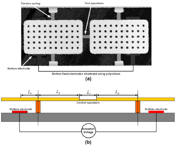
Figure 1. (a) Optical image and (b) schematic of cross-sectional view of the microstructure.
Download figure:
Standard image High-resolution image3. Mathematical modeling
3.1. Kinematic model of the proposed microstructure
Figure 2 shows the half schematic view of the microstructure with respect to the center of the test specimen. In the figure, Lp is the distance of the top suspended plate from the axis of rotation to the edge, Ls is the length of the central test specimen and Le is the distance of the center of the bottom electrode to the axis of rotation.
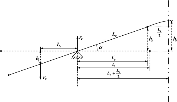
Figure 2. Schematic view of the microstructure symmetric with respect to the central test specimen.
Download figure:
Standard image High-resolution imageWith an applied actuation voltage between the top suspended plate and bottom fixed electrode, an electrostatic force acts on the plate given as;
where  is the permitivity, A is the overlap area, V is the actuation voltage, g is the air gap thickness and
  is the deflection in the top plate at the center. Under this electrostatic force, the top plate moves downwards with an angle α. From figure 2, the resultant elongation in the central specimen can be obtained as;

where  is the upwards deflection in the suspended plate at the edge and
  is the upwards defletion in the central specimen. For the test microstructure, since the stiffness of the suspended plate is much higher than the stiffness of the central of specimen, it can be assumed that the specimen undergoes a pure bending. Thus, the equilibrium equation for the central specimen can be written as;

where M is the bending moment applied to the central specimen about its thickness at a distance  from the anchor point and
  is the electrostatic force applied at a distance
  from the central specimen. The microstructure is symmetric and the idealized anchors have a reaction force
  equal to
  . The axial and bending stress in the central specimen can be evaluated by considering the deflection in the specimen under an applied electrostatic force
  . For the central specimen undergoing pure bending, the relation between the bending moment and radius of curvature can be obtained as;
where R is the radius of curvature of the central specimen, E is the Young's modulus and I is the bending moment of inertia. From figure 2, the elongation in the central specimen can be related to the radius of curvature of the central specimen under pure bending as;
The above equation shows that the radius of curvature of the central specimen with length  can be calculated by using the experimentally measured maximum deflection in the central specimen. The above equation shows that the radius of curvature of the central specimen with length
  can be calculated by using the experimentally measured maximum deflection in the central specimen. The maximum bending stress at the extreme fibers at the top and bottom of the central specimen can be obtained as;
where  is the bending moment,
  is bending moment of inertia,
  is the deflection angle, w and t are the width and thickness of the central specimen respectively. From figure 2, the reaction force acting on the central specimen corresponding to the electrostatic force
  can be calculated as;
Using above equation the axial force and hence the axial stress ( ) acting on the central specimen can be calculated by measuring the upwards defelction in th suspended plate (
 ). The equations (2), (6) and (7) shows that the total stress (
 ) and strain in the specimen can be evaluated by the experimental measure of the upwards deflection in the central specimen corresponding to an applied actuation voltage.
3.2. Elastic–plastic beam bending model
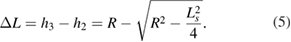
The elastic–plastic analysis in beams is generally based on the development of the 'plastic hinges'. These plastic hinges start to form when the stress at the extreme fibers of a critical section of the beam reach the yield stress value in the uni-axial tension. This results in the triangular distribution of the elastic stresses to be changed to the fully plastic rectangular stress distribution as shown in the figure 3. In the elastic region of the beam there is a linear distribution of stresses over the cross section. The maximum stress occurs at the extreme fibers and this value cannot exceed the yield stress. With an increase in the beam bending the extreme fibers yield and become plastic. This yielding continues with the applied bending unless the elastic region completely diminishes and the beam becomes fully plastic. Assuming a microbeam of symmetric cross-section A, thickness of t, having a distance of ±d from the neutral axis to the plastic region and a ratio of  ; the bending for the microbeam in the figure 3 is given as;
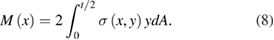
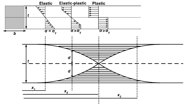
Figure 3. Elastic and elastic–plastic stress distribution and formation of the plastic hinge in a rectangular cross section.
Download figure:
Standard image High-resolution imageThe stress in the elastic region i.e.  is given by
  while the stress in the plastic region i.e.
  and
and  is equal to the yield stress
  . Thus, for a rectangular cross-section of width b(y) = b and thickness t the equation of bending can be written as;
or
The above equation shows that since at  ,
,  thus
thus  . This shows that the microbeam is in fully plastic state at
  . For
. For  and
and  ; the value of
  and hence
  . This depicts that microbeam is fully elastic for
  and
and  with a maximum stress of
  at the points
  and
and  . Similarly, for the region
  , the microbeam is in elastic–plastic region and the width of this region is determined by the value of the bending moment
  . This analysis shows that β is a function of x and hence the location of the plastic hinge varies along the length of the microbeam. For the test microstructure design presented in this work, the formation of plastic hinge can be assumed to be exactly in the center of the central specimen due to symmetric electrostatic loading and geometric shape of the central specimen.
3.3. Calculation of shape factor constant
In the elastic region, the pull-in voltage of microstructures including fixed-free microcantiliver and fixed–fixed microbeams is dependent on the structural parameters, air gap height and Young's modulus of the material along with a constant shape factor. The constant shape factor is a function of boundary conditions or geometric configuration. For example, the pull-in voltage for the fixed-free microcantiliver and fixed–fixed microbeams is given as [42]
where E, t, g, L and  are the Young's modulus, thickness, air gap height, length and air permittivity respectively for the microstructures. The equation (11) shows that the pull-in voltage is a function of same geometric parameters for the fixed-free microcantiliver and fixed–fixed microbeams with a difference of a constant shape factor value i.e. 0.47 and 2.18 for fixed-free microcantiliver and fixed–fixed microbeam, respectively. These values are verified through FEM simulations and are obtained as 0.42 for fixed-free microcantiliver and 2.2 for fixed–fixed microbeam. These results show that the constant shape factor for the central specimen in the test microstructure, presented in this work, can be estimated by considering the pull-in voltage value obtained through FEM simulations by using the following relation;
Where  is the shape factor constant,
  is the thickness of the central specimen, (
 ) is the length of the plate from the central specimen to the center of the bottom electrode. The value of
  calculated for the central specimen using equation (12) for a pull-in voltage of 118 V obtained through FEM simulations is 1.13. This value lies in between the values of shape factor constant obtained for the fixed-free microcantiliver and fixed–fixed microbeams.
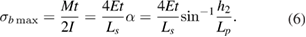
In the elasto-plastic region, the equation (12) for the pull-in voltage can be modified by introducing a β factor which incorporates the effect of plasticity. In the elasto-plastic region, the stress–strain curve can be evaluated either without considering the strain hardening effect i.e. elastic–perfect plastic behavior or with a constant strain hardening effect, as shown in figure 4. Thus, the pull-in voltage in the elasto-plastic region can be expressed as;
Where  is a ratio between the distance of the plastic hinge with respect to the central specimen neutral axis and total thickness of the central specimen. The
  is the tangent modulus that evaluates the strain hardening effect after the yield limit. As discussed in section 3.2, with β = 1 and β = 0, the central specimen is in fully elastic and plastic state respectively. However, for 0 < β < 1 the central specimen is in the elasto-plastic region.

Figure 4. Typical stress–strain curve with elastic–plastic regions.
Download figure:
Standard image High-resolution image4. Coupled field non-linear FEM modeling for the microstructures
4.1. FEM analysis for stress distribution and displacement in specimen
The stress distribution and vertical deflection in the central specimen of the test microstructures is obtained using multiphysics non-linear FEM simulations in ANSYS. The electrostatic-mechanical coupling is modeled using reduced order transducer elements (TRANS126). For the parallel plates, the fringe field capacitance is a function of (a) air gap thickness to bottom electrode width and (b) top plate thickness to bottom electrode width. The fringe field capacitance effect is more pronounced for the increasing values of these two ratios [43]. For the proposed test microstructure, the air gap thickness to bottom electrode width ratio is 0.056 and top plate thickness to bottom electrode width ratio is 0.16. These low ratio values suggest that the effect of fringe field capacitance in the FEM analysis can be ignored. Figures 5(a) and (b) shows the vertical deflection and normal stress distribution profile in the central specimen respectively, for an applied actuation voltage. The stress is mostly concentrated in the central specimen with upper and bottom surface experiencing tensile and compressive stress respectively. The stress varies linearly from bottom to the top surface with nearly zero stress in the centroid of the specimen cross-section. Moreover, the stress value in the torsion springs is negligible in comparison to the central specimen, thus minimizing the local plasticity effect in the torsion springs. Figures 6(a) and (b) shows the vertical deflection and normal stress curves for the central specimen with respect to actuation voltage. The deflection and normal stress in the specimen varies non-linearly with increasing voltage with a maximum deflection of 1.2 µm and normal stress of 177 MPa just before the occurrence of the pull-in phenomenon at 118 V. This high value stress in the specimen as compared to the yield stress of gold thin film (100–120 MPa), before pull-in, proves the suitability of the proposed design to study the plastic and elastic–plastic behavior in gold thin film.
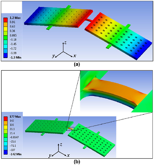
Figure 5. FEM based coupled field analysis (a) vertical deflection profile and (b) normal stress distribution in the central specimen.
Download figure:
Standard image High-resolution image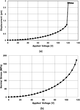
Figure 6. FEM simulations based (a) actuation voltage-vertical displacement and (b) actuation voltage-normal stress curve for the central specimen.
Download figure:
Standard image High-resolution image4.2. Validation of the kinematic model
To validate the proposed kinematic model for the test microstructures, discussed in section 3, the vertical deflection in the central specimen obtained through coupled electrostatic-mechanical analysis is used as input to the model and corresponding axial stress, bending stress and equivalent stress values are obtained. Figure 7 shows the comparison of the stress values in the central specimen obtained directly through FEM analysis with that of obtained using FEM based vertical deflection in the developed kinematic model. The results show a good correspondence between the stress values, thus validating the accuracy of the proposed kinematic model for stress evaluation in the test microstructure. Moreover, the results show that the axial stress values is negligible as compared to the bending stress in the central specimen.

Figure 7. Comparison of the stress in the central specimen obtained through FEM analysis and proposed kinematic model.
Download figure:
Standard image High-resolution image5. Experimental characterization
The static deflection in the central specimen with increasing voltage is measured using a high resolution (maximum lateral and vertical resolution of ±0.3 µm and ±0.5 × 10⁻⁴ µm, respectively) optical interferometric microscope 'ZoomSurface 3D' by Fogale Nanotech. The optical view of the test structure is converted to an elevation map using interferogram processing techniques and each pixel is associated to a grey tone corresponding to a height determined independently with nanometric accuracy in a single scan.
5.1. Characterization of test microstructure in the elastic region
Initially, one of the test microstructure is tested in the elastic region, by measuring the vertical deflection in the central specimen with increasing actuation voltage up to 100 V. As shown in figure 6(b), the actuation voltage of 100 V results in normal stress of 90 MPa in the central specimen by FEM analysis, which is fairly lower than the yield stress of the gold thin film. Thus, specimen is in the elastic region for actuation voltage up to 100 V. The test microstructure is tested for three consecutive loading cycles and corresponding vertical deflection in the central specimen is measured, as shown in figure 8. The results show that the test microstructure fully recovers to its initial position after each loading cycle and deflection for each cycle is also nearly same. Thus, with an applied actuation voltage of 100 V, with stress value of 90 MPa in the central specimen, the specimen remains in the elastic region and there is no onset of plasticity or formation of plastic hinges.

Figure 8. Experimental actuation voltage-deflection curves under repeated loading in the elastic region.
Download figure:
Standard image High-resolution image5.2. Characterization of test microstructure 2 in elastic–plastic region
For the second test microstructure, the actuation voltage is increased to 105 V to achieve higher stresses in the central specimen as compared to the first test microstructure. The normal stress value at 105 V is 110 MPa. The test microstructure is loaded for multiple cycles. Figure 9 shows that for the first loading cycle, the deflection in the central specimen with increasing voltage follows a non-linear curve with a maximum deflection of 0.7 µm at 105 V. However, for the next three loading cycles, a pull-in phenomenon occurs with a progressive decrease in the pull-in voltage value for each loading cycle. These results show that there is onset of plasticity in the specimen with an actuation voltage of 105 V and progressive decrease in the pull-in voltage value with each loading cycle can be attributed to the formation of the plastic hinge and elastic–plastic phenomenon with progressive increase in the plastic region with each loading cycle.

Figure 9. Experimental actuation voltage-deflection curve for the test structure 2 for the four loading–unloading cycles.
Download figure:
Standard image High-resolution imageThe extension in the plastic hinge and corresponding decrease in the pull-in voltage for each loading cycle, with respect to the β factor can be obtained using equation (13). Assuming that the initial stiffness of the central specimen is 98.5 GPa and strain hardening behavior is given by  = 0.6 E, the analytically calculated values of the β factor are shown in table 2. The results show a decrease in the β factor and hence decrease in the elastic stiffness for pull-in voltage values of second to fourth cycle. For the first loading cycle up to 105 V, the behavior of the specimen is fully elastic with β factor value of 1. For the second and third cycle, the β factor value progressively decreases which shows formation and extension of plastic hinge with each cycle. The pull-in voltage of 95 V for the fourth cycle, can be explained with a β factor value of 0 which shows that the specimen is in fully plastic state with extension of plastic hinge throughout the specimen.
Table 2. The progressive increase in plastic hinge for test microstructure 2 explained in terms of β factor.
| Loading cycle | Experimental Vpi (V) | Analytical model | |
|---|---|---|---|
| β Factor | Calculated Vpi (V) | ||
| First cycle | No pull in | 1 | 120 |
| Second cycle | 105 | 0.75 | 105 |
| Third cycle | 100 | 0.65 | 100 |
| Fourth cycle | 95 | 0 | 94 |
5.3. Characterization of test microstructure 3 in elastic–plastic region
To verify the elastic–plastic phenomenon for the test microstructures at an actuation voltage of 105 V, another specimen is tested for six consecutive loading cycles and deflection in the central specimen is measured. Figure 10 shows the results for the six loading cycles. At first loading cycle the deflection in the central specimen at 105 V is 0.8 µm which is same as that of test microstructure 2 for the first loading cycle. In the second and third loading cycle the specimen does not snap down at 105 V but there is a higher deflection in the central specimen as compared to the first loading cycle. For the first three loading cycle, the pull-in does not occur and the specimen seems to be in the elastic region. This behavior can be attributed to the variation in the yield point for the specimen in comparison to the second microstructure and the induced stress in the central specimen is near the yield point. However, for the fourth to sixth loading cycle the pull-in phenomenon occurs and there is also a progressive decrease in the pull-in voltage value for each loading cycle and the behavior is exactly same like the second microstructure. These results show accumulation of plastic strain in the specimen with each loading cycle with central specimen being in the elastic–plastic stress state.

Figure 10. Experimental actuation voltage-deflection curve for the test structure 3 for the six loading–unloading cycles.
Download figure:
Standard image High-resolution imageTable 3 shows the increase in the plasticity in the central specimen in terms of β factor for the six loading cycles. For the first three cycles the pull-in does not occur for loading up to 105 V. This means that the specimen is in elastic state and β factor is 1. However, for the fourth cycle the pull-in occurs at 105 V, showing initialization of the plastic hinge formation process. The corresponding β factor value is 0.75. For the fifth and sixth cycle there is a progressive decrease in the pull-in voltage value with β factor values of 0.65 and 0 respectively. This shows that the plastic hinge develops with a small localized plasticization of the specimen in the fourth cycle, expands in the next loading cycle and eventually leads to fully plasticized region in the sixth cycle with β factor value equal to 0.
Table 3. The progressive increase in plastic hinge for test microstructure 3 explained in terms of β factor.
| Loading cycle | Experimental Vpi (V) | Analytical model | |
|---|---|---|---|
| β factor | Calculated Vpi (V) | ||
| First, second and third cycle | No pull in | 1 | 120 |
| Fourth cycle | 105 | 0.75 | 105 |
| Fifth cycle | 100 | 0.65 | 100 |
| Sixth cycle | 95 | 0 | 94 |
5.4. Characterization of test microstructure 4 in elastic–plastic region
For the test microstructure 4, the static deflection in the central specimen is measured for both loading and unloading cycles. In the first loading–unloading cycle the actuation voltage is initially increased to 95 V in step by step and then decreased down to zero. The difference in the deflection values for both the loading and unloading curves is negligible and after the cycle the specimen restores to its original position as shown in figure 11. Thus showing that up to 95 V the stresses in the central specimen are in the elastic region. For the second loading–unloading cycle the actuation voltage is first increased to 105 V and maximum deflection of 0.75 µm is measured with higher deflection values for each voltage value as compared to the first loading cycle. Upon unloading to 0 V, a permanent deflection of 0.16 µm is measured for the central specimen. This shows an accumulation of plastic strain in the second loading–unloading cycle. The test microstructure is tested for the third loading–unloading cycle by increasing the actuation voltage to 110 V at which the pull-in phenomenon occurred. The actuation voltage is decreased in steps from 110 V to 0 V and pull-out voltage is observed to be 40 V. The deflection in the central specimen after third loading–unloading cycle is measured to be 0.56 µm which is much higher than the second loading–unloading cycle. This higher deflection in the central specimen can be explained with the fact that the with an actuation voltage of 110 V, the central specimen is loaded above the yield point instantaneously with the higher value of induced plasticity in the specimen. For the fourth loading–unloading cycle, the specimen snapped down at 100 V with much higher deflection at each voltage value during loading as compared to the first three cycles. The decrease in pull-in voltage value of 10 V from third to fourth cycle can be attributed to the high value of plasticity induced in the central specimen with an actuation voltage of 110 V in the preceding third cycle. During the fourth unloading, the pull-out voltage is 40 V and permanent deflection in the central specimen is 0.66 µm. Finally, the test microstructure is tested for the fifth loading–unloading cycle and a pull-in voltage of 100 V during loading and pull-out voltage of 40 V during unloading is obtained. The permanent deflection in the central specimen is measured to be 0.72 µm. The results for the second to fifth loading–unloading cycles clearly depict the onset of elastic–plastic phenomenon in the central specimen with progressive increase in the plastic strain with each loading cycle.
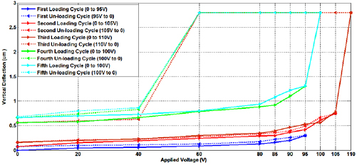
Figure 11. Experimental actuation voltage-deflection curve for fourth test structure for the five loading–unloading cycles.
Download figure:
Standard image High-resolution imageTable 4 shows the extension of plasticity in the specimen for test microstructure 4 in terms of β factor. For the first and second loading cycle where the specimen is loaded to 95 V and 105 V respectively, the pull-in does not occur. This shows that the specimen is in a fully elastic state with β factor of 1. In the third cycle, the specimen is loaded to above 105 V and pull-in occurs at 110 V. This shows the onset of plastic hinge formation with a localized plasticity with a β factor value of 0.85. The loading of the specimen for the fourth and fifth cycle shows a large decrease in the pull-in voltage i.e. 110 V for the third cycle and 100 V for the fourth and fifth cycle. This large decrease in the pull-in voltage for two consecutive cycles shows that the loading of the specimen for a voltage of 110 V in the third cycles results in fast extension of the plastic hinge and hence the pull-in occurs at a much lower value of 100 V in the next fourth and fifth cycle. Moreover, the variation in the β factor value for the central specimen in the test microstructure 4 is exactly the same as that of the specimen in test microstructure 2 and 3 i.e. with increasing the loading above the yield point the β factor value decreases progressively with a fully plasticized value of zero and corresponding pull-in of 94 V for each specimen.
Table 4. The progressive increase in plastic hinge for test microstructure 4 explained in terms of β factor.
| Loading cycle | Experimental Vpi (V) | Analytical model | |
|---|---|---|---|
| β Factor | Calculated Vpi (V) | ||
| First and second cycle | No pull in | 1 | 120 |
| Third cycle | 110 | 0.85 | 110.2 |
| Fourth and fifth cycle | 100 | 0.65 | 100 |
| 0 | 94 | ||
6. Discussion
The experimental results presented in the last section show that when the central specimen in the test microstructures is electrostatically loaded above the yield stress for multiple cycles, a progressive decrease in the pull-in voltage occurs. Moreover, the deflection in the central specimen increases with each loading cycle. The stress values higher than the yield stress in the critical areas of the central specimen results in the formation of local plasticity while other areas of the specimen are still in the elastic region. With repeated loading, the spread of plastic zone occurs and the specimen is in the elastic–plastic stress state. The increase in the permanent deflection in the central specimen with each loading cycle for test microstructure 4 explains this effect, where the actuation voltage is increased to 105 V with stress value of 110 MPa in the central specimen. This stress value of 110 MPa is close to the reported yield stress of electroplated gold thin films in literature [44–46]. Moreover, the perfectly elastic behavior of the test microstructure up to 100 V corresponding to a axial stress of 90 MPa shows that the yield stress of the gold thin film, used for fabrication of microstructures, is above 90 MPa.
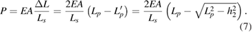
The microstructures tested for the elastic–plastic characterization in this work are fabricated using the RF switch surface micromachining process. During the microfabrication, different process steps contribute to the formation of residual stress in the microstructures. This residual stress affects both the static and dynamic response of the microstructures. Previously, authors have presented an experimental study on the effect of residual stress on static and dynamic response of RF MEMS switches and have demonstrated that the sacrificial layer removal step at 200 °C using plasma etching is the dominant step that contributes to the formation of residual stress [45]. The heating of the gold microstructures to 200 °C loads the material to the plastic state with stress values higher than the yield stress. The subsequent cooling to room temperature results in presence of induced residual stress in the microstructures. The comparison of the pull-in voltage values for the test microstructures obtained through experimental characterization and FEM simulations shows that the experimental values are lower than those of the FEM simulations. The plausible reason for this difference is the presence of residual stress in the microstructures. To investigate this effect, the plasma etching step is modeled using non-linear FEM simulations by incorporating plasticity. Figure 12 shows the non-linear stress–strain curve used in the FEM simulations with yield stress of 110 MPa, ultimate strain ( ) of 0.04, ultimate stress (
 ) of 360 MPa and tangent modulus (
 ) decreasing from 0.5E to 0.015E. After the non-linear thermal-structural analysis, a prestressed electrostatic analysis is carried out to find the pull-voltage for the test microstructure. Figure 13 shows the pull-in voltage values obtained through FEM simulations with thermally induced residual stress and experimental characterization. The results show that the pull-in voltage for the microstructures, obtained considering the residual stress, is closed to the measured experimental value.
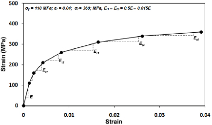
Figure 12. Stress–strain curve for the nonlinear FEM modeling considering plasticity.
Download figure:
Standard image High-resolution image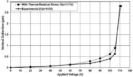
Figure 13. Comparison of the pull-in voltage values of the test microstructure.
Download figure:
Standard image High-resolution image
7. Conclusion
A simple microstructure design with a central test specimen undergoing tensile loading is presented for the analysis of elastic–plastic phenomenon in gold thin films. A kinematic model for elastic–plastic bending of the specimen is derived, which allows to calculate the stress in the central test specimen by measuring the static deflection in specimen with applied load. A constant shape factor concept for the pull-in voltage calculation of the test specimen in the microstructure is introduced and duly verified through FEM simulations. The design of microstructures presented in this work allows to achieve stress values higher than the yield stress of the gold thin film by using electrostatic actuation before the pull-in effect. An elastic behavior of the test specimen for multiple cycles actuation voltages corresponding to a stress less than 90 MPa (obtained from FEM simulations) shows that the yield stress for the gold thin films fabricated using RFS micromachining process with gold layer thickness of 2.5–3.2 µm is above 90 MPa. The progressive decrease in the pull in voltage of the test microstructures once actuated up to 105 V (that corresponds to 110 MPa in the test specimen) for multiple cycles, demonstrates elastic–plastic phenomenon in the test microstructures. The progressive decrease in the pull-in voltage value for each loading cycle is explained by introducing a β factor that relates the onset of plastic hinges and its extension under repeated loading to the pull-in voltage value. The results show that when the stress in the specimen is lower than the yield point the specimen behaves elastically under repeated loading. In particular with β factor value of 1. However, with loading above the transition voltage (above 105 V) the stresses in the specimen exceed the yield point and result in initiation of a plastic hinge in the center. With increasing loading cycles, the specimen eventually becomes fully plasticized with β factor value of 0 and corresponding pull-in voltage value of 94 V. For the next loading cycles, the extension in the plastic hinge occurs with increased plasticity and evaluated with an analytical parameters value. With increasing loading cycles, the specimen eventually becomes fully plasticized and the non-dimensional parameter shows the increasing of the bending plastic hinge formation.
Acknowledgments
Authors thank Bruno Kessler Foundation of Trento and in particular Dott B Margesin for the support in the realization of specimens.