
Abstract
Finite element simulation was used to analyze the effect of electric boundary conditions on the indentation deformation of a transversely isotropic piezoelectric film with the contact radius much larger than the film thickness. Six different combinations of electric boundary conditions were used. The simulation results showed that the indentation load is proportional to the square of the indentation depth and the indentation-induced electric potential at the contact center is a linear function of the ratio of the indentation depth to the film thickness for all six cases. The contact stiffness is proportional to the contact area and inversely proportional to the film thickness. The nominal piezoelectric charge coefficient d33 is inversely proportional to the derivative of the electric potential with respect to the indentation depth for the indentation of a piezoelectric film by a conducting indenter with a grounded, rigid substrate.
Export citation and abstract BibTeX RIS
1. Introduction
Piezoelectric materials with the characteristics of electromechanical coupling are available in a variety of shapes and forms, such as films [1–3], multi-layers [4] and fibers [5–8] for various sensor and actuator applications in functional structures and smart systems [9–13]. Accurate determination of the material behavior of piezoelectric materials at the small scale is vital for applications in microelectromechanical and nanoelectromechanical systems. The instrumented indentation technique, which has been used to determine the mechanical properties of small structures and thin films, is believed to be capable of characterizing the mechanical as well as electrical properties of piezoelectric materials [14–18].
To date, most analytical and numerical studies have focused on the indentation of a piezoelectric half-space [19–30]. However, compared to the indenter size and the specimen thickness, piezoelectric films have finite thickness rather than infinite thickness in engineering and biomechanical applications, and it is known that simplified solutions can be obtained when the contact radius is much larger than the film thickness [31–36]. Thus, it is desirable to probe the material properties of piezoelectric ceramics by indenting piezoelectric thin films, in which the contact radius is far greater than the film thickness.
Using the Hankel transform and a conducting indenter, Matysiak [19] was the first to study the axisymmetric contact of a piezoelectric half-space. Following Matysiak's approach [19], Giannakopoulos and Suresh [23] presented a general solution for the axisymmetric indentation of a piezoelectric half-space. Although their analytical solutions have the same structures as those given by Chen et al [21], Kalinin et al [26] and Wang et al [36], they are numerically different. Wang et al [36] studied the indentation of piezoelectric films and suggested that the expressions given by Giannakopoulos and Suresh [23] are problematic. In addition, the boundary condition with zero normal stress at the edge of the contact zone [23] is inapplicable for a flat-ended indenter, since there is stress singularity [37]. Sridhar et al [38] performed the normal indentation of a transversely isotropic, linear piezoelectric half-space by a conducting sphere with zero potential bias and found that the indentation response of piezoelectric materials depended on the electric boundary conditions. Yang [30] derived the contact stiffness, effective piezoelectric constant and electric displacement intensity factor for the axisymmetric indentation of a semi-infinite piezoelectric material by a rigid, conducting indenter of arbitrary axisymmetric profile and found that analytical solutions cannot be obtained for certain combinations of material properties of piezoelectric materials. Ding et al [24] solved the elastic and electric fields for a series of axisymmetric contact problems, including the press of a spherical indenter, a conical indenter and an upright circular flat indenter onto a transversely isotropic piezoelectric half-space. Yang [39] analyzed the electromechanical interaction between a compliant surface electrode and a semi-infinite piezoelectric material. Wang and Han [28] used frictionless conditions between a piezoelectric layer and a rigid substrate to numerically simulate the deformation of the piezoelectric layer indented by a flat-ended cylindrical indenter. Kamble et al [18] simulated the spherical indentation of polycrystalline PZT-4 and misused the zero electric potential condition on the axial axis in the finite element analysis. Liu and Yang [40] performed a finite element simulation of the spherical indentation of a transversely isotropic piezoelectric half-space by a conducting or insulting spherical indenter and developed semi-empirical relations between the indentation load and the indentation depth and between the electric potential on the indenter and the indentation depth, respectively, for indentation by a rigid, conducting indenter.
Motivated by the practical applications of piezoelectric films and the need to have a better understanding of the indentation behavior of piezoelectric films, a systematic finite element analysis of the spherical indentation of a piezoelectric film is carried out. The focus is on the effect of electric boundary conditions on the contact deformation of piezoelectric films with the contact radius much larger than the film thickness. The dependence of the electric response on the indentation deformation is also discussed.
2. Problem formulation
Consider the indentation of a transversely isotropic piezoelectric film of thickness t by a rigid spherical indenter of radius R. As shown in figure 1, the piezoelectric film is supported by a rigid substrate with the non-slip condition. A cylindrical polar coordinate system (r,θ,z) is used with the z-axis being parallel to the poling direction. The r-axis is perpendicular to the z-axis, and θ is the azimuth angle between a reference line and the r-axis. In the absence of body and inertia forces, the equilibrium equations for the axisymmetric problem are


and in the absence of free electric charge in the piezoelectric film the electrostatic equation is

where σrr, σzz, σθθ and σrz are the components of the stress tensor, and Dr and Dz are the components of the electric displacement vector.
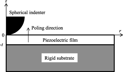
Figure 1. Schematic of the spherical indentation of a piezoelectric film on a rigid substrate.
Download figure:
Standard imageFor linear transversely isotropic piezoelectric materials with the poling direction parallel to the z-axis the constitutive equations in the absence of any thermal or residual polarization strains with conventional notations are
where C11, C12, C13, C33 and C44 are the elastic constants measured in a constant electric field intensity (short circuited condition), e15, e31 and e33 are the piezoelectric constants measured in a spontaneous electric field and ∈11 and ∈33 are the dielectric constants measured with no mechanical constraint. The subscript '3' denotes the properties along the poling direction and the subscripts '1' and '2' denote the properties along two mutually orthogonal directions in the plane perpendicular to the poling direction.
The relationships between the components of the strain tensor (εrr, εθθ, εzz and εrz) and the components of the displacement vector (ur and uz) are
and the relationships between the components of the electric field intensity (Er and Ez) and the electric potential (ϕ) are

The indentation load can be determined from the force balance on the indenter as

During the indentation, the contact radius monotonically increases with the indentation load. This requires dF/dh > 0 for h > 0.
The conditions at infinity require

Mechanical boundary conditions
For the contact problem of a transversely isotropic piezoelectric film ( − t < z < 0, t is the film thickness) with a rigid, spherical indenter, the mechanical boundary conditions are


where h is the indentation depth of the indenter, a is the contact radius and f(r) is the surface profile of the indenter. For an indentation by a rigid spherical indenter of radius R with a ≪ R
For frictionless contact between the indenter and the film, the shear stress is zero, i.e.

The non-slip contact between the film and the rigid substrate gives

The condition determining the contact radius a is

Electric boundary conditions
Two types of indenter are used in the finite element analyses. They are as follows.
Case I. Insulating indenter.
The electric boundary condition on the surface of the piezoelectric material for indentation by an insulating indenter is

Case II. Conducting indenter.
For a conducting indenter without a prescribed electric potential the electric potential within the contact region is a constant. The electric boundary condition on the surface of the piezoelectric material becomes


For a grounded conducting indenter one has

which has technological advantages for the application of the sharp-instrumentation indentation in characterizing the properties of piezoelectric materials.
The indentation-induced electric charge, Qp, within the contact area on the top surface of the piezoelectric film can be calculated by integrating the normal component of the electric displacement, Dz(r,0), within the contact area as

which gives the total charge accumulated in the conducting indenter as

For an insulating substrate

and for a grounded substrate

There are six possible combinations of the electric boundary conditions (II, IG, CI, CG, GI and GG). II corresponds to the insulating indenter and the insulating substrate, IG to the insulating indenter and the grounded substrate, CI to the conducting indenter without prescribed electric potential and the insulating substrate, CG to the conducting indenter without prescribed electric potential and the grounded substrate, GI to the grounded indenter and the insulating substrate and GG to the grounded indenter and the grounded substrate.
It needs to be emphasized that the simulation focuses on the contact radius being much larger than the film thickness and there is no transfer of free charges between the indenter and the piezoelectric film.
It is known that the distribution of electric field depends on the geometrical morphology of a material. Puglisi and Zurlo [41] analyzed the effect of surface curvature on electric field localization in thin dielectric films and obtained an approximate expression for the electric field. Yang and Song [42, 43] analyzed the field-induced surface instability of a conducting material with a sinusoidal surface topology by analyzing the effect of the sinusoidal surface on the field and stress distribution. Generally, one needs to include the effect of local curvature on the electric field in the analysis. However, the analysis of the indentation deformation is based on the linear theory of piezoelectricity, which requires that the boundary conditions including the electric boundary conditions be referenced to the undeformed state. In numerical calculations, such as finite element simulation, the electric boundary conditions are actually satisfied at each increment.
3. Finite element simulation
To simulate the indentation deformation, the nonlinear deformation feature in the ABAQUS finite element code is used. Transversely isotropic piezoelectric materials, which have axisymmetric features about the poling direction, are used. The material properties of PZT-4 given in table 1 are used in the simulation. The rigid indenter of 500 μm in radius is modeled by a rigid, analytical surface. The dimensions of the piezoelectric material used in the simulation are 200μm in radius and 0.5 μm in thickness. The maximum indentation depth of 50 nm is only 10% of the film thickness, which avoids any severe deformation that may introduce depolarization or cracking during indentation, and the indentation depth of 50 nm is believed to be non-destructive to the sample.
Table 1. The material properties of PZT-4 piezoelectric ceramic [39].
| Elastic constant (1010 N m−2) | Piezoelectric constant (C m−2) | Dielectric constant (10−10 C V−1 m−1) | |||||||
|---|---|---|---|---|---|---|---|---|---|
| C11 | C12 | C13 | C33 | C44 | e31 | e33 | e15 | ∈11 | ∈33 |
| 13.9 | 7.78 | 7.43 | 11.3 | 2.56 | − 6.98 | 13.84 | 13.44 | 60.0 | 54.7 |
Due to the symmetric feature, the axisymmetric model is used. Figure 2 shows the finite element mesh near the contact zone. The finite element mesh consists of 125 708 four-node axisymmetric piezoelectric elements. Finer meshes are used near the contact region. The surface of the sphere is automatically smoothed to reduce the inaccuracy in calculating the contact stress. Along the interface, the contact elements are used to monitor the change of the contact zone during the indentation. For the conducting indenter or substrate the nodes within the contact region or on the interface are constrained by the equal electric potential and for the grounded conducting indenter or substrate the nodes within the contact region or on the interface are constrained with zero electric potential.
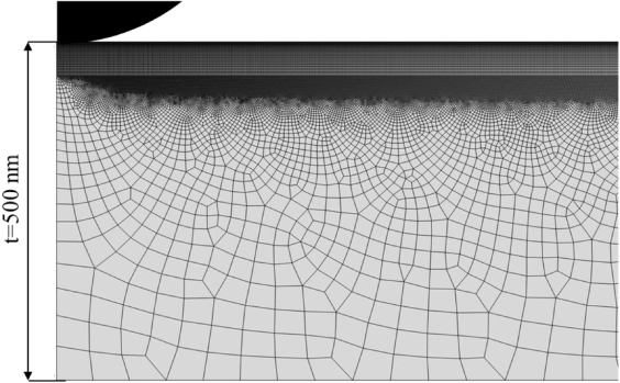
Figure 2. The finite element mesh of the spherical indentation.
Download figure:
Standard imageA displacement-controlled indentation is used in the simulation. The indenter is gradually pushed onto the surface of the piezoelectric material to a preset indentation depth and then it is withdrawn until the load on the indenter becomes zero. During the indentation, the equal-potential condition for indentation by a conducting indenter is checked at each increment to ensure that the nodes in contact with the conducting indenter have the same electric potential.
4. Results and discussion
4.1. Mechanical response
The contact radius is a function of the indentation depth, and the closed-form solutions of the contact radius for the indentation of thin films with t ≪ a ≪ R have been obtained only for two cases. Wang et al [36] obtained the dependence of the contact radius on the indentation depth for the indentation of a transversely isotropic piezoelectric film by an insulating indenter with a grounded, rigid substrate as

and for the indentation of a piezoelectric film by a conducting indenter of potential ϕ0 with a grounded, rigid substrate as
Equation (24) reduces to equation (23) for a grounded, conducting indenter, i.e. ϕ0 = 0.
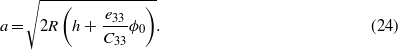
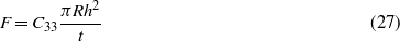
Figure 3 shows the variation of the contact radius with the indentation depth for all six different combinations of electrical boundary conditions. The overlap of the curves indicates that the variation of the contact radius with the indentation depth for the spherical indentation of a piezoelectric film is independent of the electric boundary conditions given in section 3. For h/t ≥ 0.01, the relationship between the contact radius and the indentation depth can be described by equation (23), while for h/t < 0.01, equation (23) overestimates the contact radius due to the constraint of a ≫ t. At h/t = 0.01, a = 4.78 × 10⁻³ R = 4.78t. This result suggests that equation (23) can be used to determine the contact radius from the indentation depth when a ≥ 4.78t.
Figure 3. (a) Variation of the contact radius with the indentation depth for six different electric boundary conditions; (b) enlarged view of the contact radius–indentation depth curves for 0.02 ≤ h/t ≤ 0.1.
Download figure:
Standard imageFor the spherical indentation of a piezoelectric half-space the relationship between the contact radius and the indentation depth is [30]

which is independent of the type of indenter (insulating or grounded, conducting indenter). For comparison, equation (25) is also included in figure 3. Obviously, equation (25) describes the indentation depth–contact radius relationship for h ≪ t and a ≪ t.
The indentation load–depth relationship has been used to determine the reduced contact modulus for the instrumentation indentation technique. According to the results given by Wang et al [36], the relationship between the indentation load and the indentation depth is
for the indentation of a transversely isotropic piezoelectric film by an insulating indenter with a grounded substrate, i.e. the IG case, and
for the indentation by a grounded, conducting indenter with a grounded substrate, i.e. the GG case. Independently of the electric boundary conditions, the indentation load is proportional to the indenter radius and the square of the indentation depth and inversely proportional to the film thickness, which is similar to the results given by Yang [32, 33] for the spherical indentation of compressible, elastic films with the contact radius much larger than the film thickness. The effect of the electric boundary conditions is represented by the coefficients.
Figure 4 shows the indentation load–depth curves for all six different combinations of electrical boundary conditions. For comparison, the results calculated from equations (26) and (27) are also included. The finite element results are in good agreement with the analytical results for the corresponding boundary conditions. The electric boundary conditions have some effect on the dependence of the indentation load on the indentation depth, since the curves slightly differ from one another. The indentation load in general increases with the square of the indentation depth for all six cases under the simulation conditions. To produce the same indentation depth, the smallest indentation load is needed for the indentation by a grounded, conducting indenter with a grounded substrate, while the largest indentation load is needed for the indentation by an insulating indenter with an insulating substrate. Comparison of the dependence of the indentation load on the indentation depth for all six cases reveals that the force responses can be divided into two categories; one is associated with the grounded, conducting indenter and the other is related to the indentation by an insulating indenter or a conducting indenter without a prescribed potential.
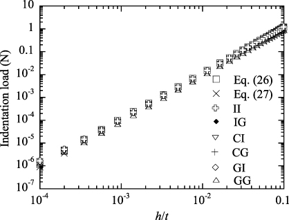
Figure 4. The dependence of the indentation load on the indentation depth for six different electric boundary conditions.
Download figure:
Standard imageIt is worth mentioning that the finite element analysis of the spherical indentation of a transversely isotropic piezoelectric half-space by a conducting or an insulating indenter was performed by using the ABAQUS finite element code [40]. The simulation results are in good accord with the results given by the analytical relationships between the indentation load and the indentation depth as summarized by Wang et al [36] and given by Ding et al [24], which have validated the finite element code used in this work.
From equations (26) and (27) and the simulation results shown in figure 4, one can express the relationship between the indentation load and the indentation depth for all six cases as
where χ is a function of the material properties of the piezoelectric material and the electric boundary conditions. Equation (28) gives the contact stiffness, S, as

for the spherical indentation of transversely isotropic piezoelectric films with the contact radius much larger than the film thickness. Here,  for the indentation by an insulating indenter with a grounded substrate and χ = C33 for the indentation by a grounded, conducting indenter with a grounded substrate. The contact stiffness is proportional to the contact area A and inversely proportional to the film thickness in contrast to the result for the spherical indentation of semi-infinite piezoelectric materials. Equation (29) provides an approach to measure the electromechanical properties of piezoelectric films by controlling the electric boundary conditions.
For the indentation of a transversely isotropic piezoelectric film with the contact size much larger than the film thickness, the distribution of normal stress over the contact area (0 ≤ r ≤ a) is [36]
for the spherical indentation by an insulating indenter with a grounded substrate (i.e. the case of IG) and

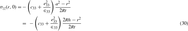
for the spherical indentation by a grounded indenter with a grounded substrate (i.e. the case of GG). Both the stress distributions in the contact zone are quadratic functions of the radial variable r. Figure 5 shows the finite element results for the distribution of the normal stress in the contact zone for all six cases with a maximum indentation depth of 50 nm. For comparison, the analytical results of equations (30) and (31) are also included in figure 5. For the spherical indentation by an insulating indenter or a grounded indenter with a grounded substrate, the magnitudes of the normal stress obtained from the FEM simulation are in good accord with the corresponding analytical results for r/t ≥ 7 and slightly larger than the corresponding analytical results for r/t < 7. Such behavior is due to the condition used in deriving equations (30) and (31), which requires a/t ≫ 1, even though it has no significant effect on the load–displacement relationship. As shown in figure 5, the piezoelectric material experiences compressive stress, as expected, with the maximum compressive stress being at the contact center. For the same indentation depth and a spherical indenter of the same size the indentation by an insulating indenter with an insulating, rigid substrate produces the largest compressive stress in the contact zone, while the indentation by a grounded indenter with a grounded, rigid substrate produces the smallest compressive stress. Due to the singularity of the electric field, the indentation by the conducting indenter creates a stress singularity at the contact edge, which is likely to lead to structural damage.
Figure 5. The distribution of the normal stress on the top surface of the piezoelectric material for six different electric boundary conditions with an indentation depth of 50 nm.
Download figure:
Standard image4.2. Electric response
The dependence of the indentation-induced electric potential at the contact center on the indentation depth is depicted in figure 6. The magnitude of the electric potential at the contact center increases with increasing indentation depth, which is in accordance with the mechanism of piezoelectric behavior. For the same indentation depth the indentation by the insulating indenter with a grounded, rigid substrate induces the largest electric potential at the contact center, while the indentation of the piezoelectric film by the conducting indenter with an insulating, rigid substrate induces the smallest electric potential. These results suggest that the electric boundary conditions determine the electric response of the piezoelectric film during indentation. For h/t ≥ 0.02 the indentation-induced electric potential at the contact center is a linear function of the ratio h/t for any contact radius larger than the film thickness, i.e.

where ϕc is the electric potential at the contact center and α and κ are constants depending on the material properties and the electric boundary conditions. Through the best curve-fitting, one can calculate the α and κ constants from the FEM results. For the indentation by a conducting indenter without a prescribed potential the indentation-induced potential on the indenter then can be calculated from equation (32) if the constants α and κ have been determined from the numerical calculation or from the indentation test of piezoelectric films by characterizing the variation of the contact potential with the indentation depth.
Figure 6. The dependence of the electric potential at the contact center on the indentation depth for four different electric boundary conditions.
Download figure:
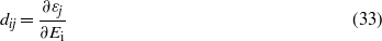
Standard imageAccording to the definition of piezoelectric charge coefficients, dij [44],
in which εj is the matrix representation of εij with ε1 = ε11, ε2 = ε22, ε3 = ε33, ε4 = 2ε23, ε5 = 2ε13 and ε6 = 2ε12. For the indentation of piezoelectric films by the conducting indenter with the grounded substrate and the contact radius much larger than the film thickness the compressive strain underneath the indentation can be approximated as

and the magnitude of the electric field intensity as

Substituting equations (34) and (35) into (33) and using the condition of h ≪ t, the piezoelectric charge coefficient, d33, can be determined by
The nominal piezoelectric charge coefficients as determined from the indentation of a piezoelectric film by a conducting indenter with a grounded, rigid substrate and the contact radius much larger than the film thickness are inversely proportional to the derivative of the electric potential with respect to the indentation depth.
Due to the electromechanical coupling in piezoelectric materials, the indentation deformation by the conducting indenter will polarize the piezoelectric material and lead to accumulation of electric charges on the conducting indenter. The total charge accumulated on the surface of the conducting indenter can be calculated from equation (20). Figure 7 shows the variation of the total charge with the indentation depth for the indentation by the conducting indenter. The total electric charge increases with increasing indentation depth due to the piezoelectric coupling. For the same indentation depth the largest total charge accumulated on the conducting indenter is induced when the indenter is grounded, while the smallest total charge is induced for the indentation with an insulating substrate. The electric boundary conditions play an important role in controlling the accumulation of electric charges on the conducting indenter.
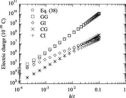
Figure 7. The variation of the total electric charges accumulated on the conducting indenter with the indentation depth for four different electric boundary conditions.
Download figure:
Standard imageFor the indentation of the piezoelectric film with a grounded substrate the simulation results shown in figure 7 suggest that, for h/t ≥ 10−3, the total charge accumulated on the conducting indenter is a power function of the ratio of h/t. Using the best curve-fitting one obtains
with n = 2 for the indentation by a grounded indenter with a grounded substrate and n = 1.5 for the indentation by a conducting indenter without a prescribed potential and with a grounded substrate. Here β is a constant depending on the material properties and the electric boundary conditions.
Using the result given by Wang et al [36] for the grounded indenter and the grounded substrate with the poling direction being anti-parallel to the loading direction, the total charge is found to be

For comparison, the calculated results from equation (38) are also included in figure 6. Obviously, the simulation results are in agreement with those calculated from equation (38) for h/t ≥ 10−2. For the spherical indentation of piezoelectric films by a grounded, conducting indenter with a grounded substrate and the contact radius much larger than the film thickness equation (38) can be used to determine the piezoelectric constant e33.
For the indentation by a grounded indenter with a grounded, rigid substrate and a ≫ t one can use the result given by Wang et al [36] to obtain the distribution of the normal component of the electric displacement in the contact zone as

in which the sign of ± depends on the relative direction between the loading direction and the poling direction (axisymmetric axis). For the current configuration with the loading direction anti-parallel to the poling direction the ' − ' is used in equation (39). The normal component of the electric displacement is a quadratic function of the radial variable r. Figure 8 depicts the distribution of the normal component of the electric displacement for all the six different boundary conditions with the maximum indentation depth of 50 nm. For comparison, the results obtained from equation (39) are also included in figure 8; these are slightly lower than the FEM results near the contact center, while there is good agreement in the region away from the contact center.
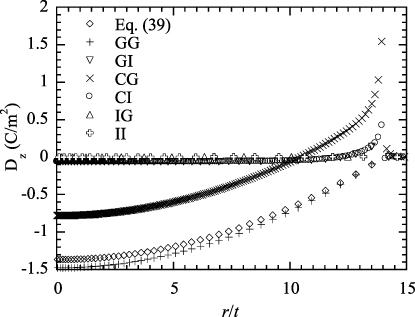
Figure 8. The distribution of the normal component of the electric displacement on the top surface of the piezoelectric material for six different electric boundary conditions with an indentation depth of 50 nm.
Download figure:
Standard imageFor the indentation by an insulating, rigid indenter the normal component of the electric displacement is zero, as expected. There exists a transition of the normal component of the electric displacement from a negative value to a positive value for the other four types of electric boundary condition, i.e. CI, CG, GI and GG. Field singularity is observable for the indentation by a conducting indenter due to non-zero potential on the indenter, which leads to the stress singularity at the contact edge as shown in figure 5. It is worth mentioning that the field singularity has not been reported for the indentation of piezoelectric films, even though the same behavior has been observed from the finite element simulation of semi-infinite piezoelectric materials by Liu and Yang [40].
Figure 9 shows the distribution of electric potential on the contact surface between the indenter and the piezoelectric film for all the six electric boundary conditions with a maximum indentation depth of 50 nm. The electric potential for the grounded indenter is zero in the contact zone, as expected. The distribution of electric potential depends on the electrical boundary conditions. The indentation by the conducting indenter produces uniform, non-zero electric potential on the contact surface. The magnitude of the indentation-induced potential is a function of the electric condition of the rigid substrate with the grounded substrate generating a smaller magnitude of electric potential than that of the insulating substrate at the contact center. Non-uniform electric potential is created for the indentation by the insulating indenter, which is relatively independent of the electric condition of the substrate.
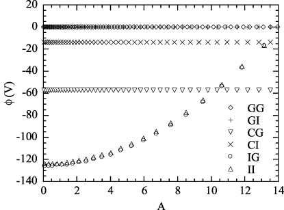
Figure 9. The distribution of the electric potential on the top surface of the piezoelectric material for six different electric boundary conditions with an indentation depth of 50 nm.
Download figure:
Standard imageThe above analyses have established the rationale of using the sharp-instrumented indentation to characterize the complicated electromechanical interaction of piezoelectric films. The load–displacement relationship and the load–potential relationship can be used to quantify the piezoelectric behavior of piezoelectric films similarly to the work by Kollosche and Kofod [45] by using the contact technique to examine the dependence of the breakdown strength of soft elastomers on Young's modulus. Careful comparison between the FEM results and experimental results will be explored in the future.
5. Summary
Finite element analysis of the indentation deformation of piezoelectric films with the properties of PZT-4 by a rigid, spherical indenter revealed the effects of different electric boundary conditions on the mechanical and electrical responses of piezoelectric thin films. Six different combinations of the electric boundary conditions between the indenter and the film and between the film and the substrate were used to investigate the effect of electric boundary conditions on the electrical and mechanical responses of the piezoelectric film when the contact radius is much larger than the film thickness.
The indentation load was found to be proportional to the square of the indentation depth for all six cases, with the smallest indentation load being required to produce the same indentation depth for the indentation by a grounded, conducting indenter with a grounded substrate and the largest indentation load for the indentation by an insulating indenter with an insulating substrate. For h/t ≥ 0.01 the contact radius is proportional to the square root of the indentation depth and is independent of the electric boundary conditions. A simple formula was established for the calculation of the contact stiffness, which is proportional to the contact area and inversely proportional to the film thickness in contrast to the result for the spherical indentation of semi-infinite piezoelectric materials.
For h/t ≥ 0.02 the indentation-induced electric potential at the contact center is a linear function of the ratio of h/t for the contact radius larger than the film thickness with the slope κ being dependent on the electric conditions. For the indentation by a conducting indenter with a grounded substrate and h/t ≥ 10−3 the total charge accumulated on the indenter is a power function of the ratio of h/t. The nominal piezoelectric charge coefficient d33 is inversely proportional to the derivative of the electric potential with respect to the indentation depth for the indentation of piezoelectric films by a conducting indenter with a grounded, rigid substrate.
Acknowledgment
This work is supported by NSF through Grant No. CMMI-0800018.