
Abstract
Through-silicon via (TSV) is an emerging technology for three-dimensional integrated circuit, system-in-packaging and wafer-level packaging applications. Among several available TSV formation methods, Bosch deep reactive ion etching (DRIE) is widely used because it enables the fabrication of TSVs with almost any diameter, from the submicrometer level to hundreds of micrometers. However, the high cost of Bosch DRIE makes it uneconomical for industrial production. We present a novel wafer-level TSV formation approach that is effective and cost-efficient. The proposed method integrates a diode-pumped solid-state ultraviolet nanosecond pulsed laser and rapid wet chemical etching. The former is effective in drilling through 400 µm thick silicon wafers and the latter is used for removing the unwanted heat-affected zone, recast layer and debris left after drilling. Experimental results demonstrate that the combined approach effectively eliminates the unwanted material formed by nanosecond laser pulses. Furthermore, this approach has a significant cost advantage over Bosch DRIE. In summary, the proposed approach affords superior TSV quality, higher TSV throughput and lower cost of process ownership than Bosch DRIE. These advantages could provide the necessary impetus for rapid commercialization of the several high-density fabrication methodologies that depend on TSVs.
Export citation and abstract BibTeX RIS
1. Introduction
Through-silicon vias (TSVs) are particularly effective for establishing interconnections in technologies such as three-dimensional integrated circuits (3D ICs), system-in-packaging and wafer-level packaging (WLP). They can be used to interconnect devices vertically and thus shorten the length of interconnections, increase the input/output density, lower resistance and reduce parasitic inductance [1–4]. However, the high cost involved in the formation of TSVs still limits their application in advanced technologies. To overcome this economic bottleneck, particularly in WLP technology, the development and adoption of a low-cost wafer-level (WL) TSV formation approach are highly anticipated.
WLP technologies include the key fabrication processes of TSV formation, TSV isolation, TSV filling and die dicing [5]. Redistribution of TSVs on wafers for WLP applications usually necessitates a straight and smooth profile and a tapered slope of between 85° and 90° to facilitate subsequent metallization. Moreover, the optimal diameter of the TSVs will vary according to the application [6]. Thus, one of the key challenges for the development and adoption of the next generation of packaging technologies is the reliable formation of TSVs for products such as light-emitting diodes (LEDs) [7], dynamic random access memory capacitors [8], micro-electromechanical systems [9, 10], and complementary metal–oxide–semiconductor image sensors [11]. TSV formation methods include inductive coupled plasma [12–14], Bosch deep reactive ion etching (DRIE) [13–18], wet etching [14, 19] and laser drilling [6, 20–23], among others. Of these, the Bosch DRIE process is the most commonly used method [14, 24].
However, the scalloped profile produced by Bosch DRIE will cause problems in subsequent metal filling in TSV applications. The conventional Bosch DRIE process normally produces a high sidewall scallop of 100–200 nm. According to the latest literature, optimization of etching and passivation time can reduce this scallop to obtain a sidewall roughness of 10 nm, with a maximum silicon etching rate of 4 µm min−1 [13–18]. Clearly, the etching rate is far from sufficient to meet the requirement of high-speed deep TSV fabrication for WLP technology because an etch depth of more than 100 µm is necessary for several applications. Moreover, these applications usually require a wide range of etch depths, ranging from a few to several hundred micrometers [25]. Therefore, the TSV formation process requires a high etching rate to produce smooth and high-throughput sidewalls that ensure the optimal filling of conducting materials in subsequent processes, and to reduce the cost so as to meet the requirements for industrial production. These demands present great challenges to deep silicon etching for TSVs [14]. With the aim of responding to these challenges, we devise a novel approach that integrates laser drilling and wet chemical etching (WCE) in this paper.
The advantages of laser drilling over Bosch DRIE are in the flexibility of pattern design and low cost of equipment. The latest laser technology, femtosecond (fs) pulsed laser, could have the potential to fabricate well-shaped TSVs with sidewalls of excellent quality. However, high-power fs lasers are still under development, and commercially available fs lasers lack the power and stability to provide an acceptable throughput for mass production. Instead, a diode-pumped solid-state (DPSS) ultraviolet (UV) laser with nanosecond (ns) pulses would be more efficient in mass production.
Unfortunately, laser ablation with ns pulses causes not only thermal but also mechanical damage to the wafer surface and TSV sidewall because the laser beam interacts with the solid, liquid, vapor and plasma phases at or near the material surface [26]. Rapid WCE would be a useful support process to overcome this major drawback while maintaining the exceptional efficiency of ns lasers. WCE of silicon with HF–HNO3 mixtures is a widely used process in the semiconductor industry and in the production of solar cells [27, 28]. This hybrid approach would feature pre-machining by rapid laser ablation without tool wear and post-machining with an optimal WCE process.
In this study, we investigated the feasibility and characteristics of this novel approach for a WL LED sub-mount application. The drilling quality, drilling efficiency and cost of ownership of the TSV formation approach were evaluated in comparison to those of the Bosch DRIE process. In addition, to obtain optimal WCE performance, three aqueous chemical etchants were investigated and their experimental parameters were optimized prior to the experiments.
2. Experimental setup
2.1. Designed pattern layout
To redistribute WL TSVs on wafers for the LED sub-mount application, a layout pattern with 9400 TSVs wafer−1 was designed for WLP. Moreover, the specifications like the wafer thickness of 400 µm, TSV diameter of 150 µm and taper angle of the TSV sidewall between 85° and 90° are required. The bending strength of the silicon wafer is only around 250 MPa; hence, the 400 µm thick silicon wafer is necessary to prevent fracture of the silicon substrate in the subsequent packaging process. The TSV diameter in 3D ICs for achieving the highest volume capacity ratio is around 50 µm; however, in the LED sub-mount application, heat dissipation is of great concern. TSVs of larger diameter that contain holes filled with copper electroplating are beneficial for overcoming the problem of LED heat dissipation. Copper electroplating is a critical process after TSV formation. A taper angle between 85° and 90° is the best condition for rapid electroplating and metal coherence. The copper peels if metal coherence fails. In brief, the purpose of the designed pattern layout and specification of TSVs is to improve the performance and reliability of production.
2.2. Laser drilling with ns pulses
The experiments were carried out by using a DPSS UV ns pulsed laser. The laser source used in this study was a commercially available Q-switched, DPSS industrial ns UV laser that delivers an average power of 14 W at 100 kHz with a 355 nm wavelength and 40 ns pulse width. To drill through a thick wafer efficiently, the laser beam was focused through a telecentric lens with a focal length of 100 mm to achieve a 25 µm spot size with a depth of focus of approximately 400 µm. A two-axis galvanometer was used to quickly position the laser beam from point to point with a scan field of 50 mm × 50 mm on the X–Y plane. Trepanning, a process in which a laser beam smaller than the target diameter is moved in a circular motion to cut out holes, was then performed with ns laser pulses to afford TSVs with the following desired specifications: well-shaped holes, a taper angle of 85°–90° and a diameter of 100 µm. The laser drilling parameters were optimized in advance by the technical engineers of Marketech International Corporation (MIC), Taiwan. The tested samples were p-type single-crystal silicon wafers polished on one side with (1 0 0) crystal orientation, a diameter of 200 mm (8''), and a thickness of 400 µm. A confocal microscope (CM) and scanning electron microscope (SEM) were used to study the characteristic features of the TSVs, their surfaces and changes in the surroundings of the laser-drilled TSVs. The specifications of the laser system, drilling materials, optimized processing parameters and target values in this study are summarized in table 1.
Table 1. Specifications of laser system, parameters, materials and target values.
| Features | Parameters | Values |
|---|---|---|
| DPSS UV | Wavelength | 355 nm |
| Average power | 14 W | |
| Frequency | 100 kHz | |
| Pulse width | 40 ns | |
| Beam speed | 250 mm s−1 | |
| Beam diameter | 25 µm | |
| Depth of focus | 400 µm | |
| Drilling method | Trepanning | |
| Drilling target | Diameter | 100 µm |
| Taper angle | 85°–90° | |
| Drilling speed | 5–10 TSVs s−1 | |
| Material | Size | 200 mm |
| Wafer thickness | 400 µm |
2.3. Wet chemical etching
WCE of silicon with HF–HNO3 mixtures is widely used in the semiconductor industry and in the production of solar cells [27, 28]. The etching mechanism has been systematically investigated in several studies [29–31], according to which the etching of silicon in HF/HNO3 mixtures follows a chemical process with two basic reaction steps. In the first step, silicon is formally oxidized by HNO3 (equation (1)). In the subsequent step, the formed SiO2 is dissolved by HF (equation (2)). The overall reaction is written as (equation (3)):


The advantages of the WCE process are its simplicity, low cost, high yield rate and high etching selectivity. The etchants for the isotropic etching of silicon materials are mostly mixtures of HF, HNO3, H2O, CH3COOH and NH4F. Each etchant, which will have a different etching rate depending on the particular combination of etchants, is characterized by a unique etching selectivity. As a result, various degrees of surface finish can be achieved.
In this study, WCE was employed to remove surface or sidewall damage due to laser drilling on wafers. The laser-drilled wafers were laid horizontally and etched for 40 s in a polypropylene tank with the polished surface facing upward, and the etchant was magnetically stirred at 300 rpm and 20 °C. Three aqueous chemical etchants—etchants A (HF, HNO3 and H2O), B (HF, HNO3 and CH3COOH), and C (HF, HNO3 and NH4F)—were investigated. The chemical etchants were optimized for the purposes of cleaning debris, removing recast layers and providing the optimal conditions of wafer surface and sidewall roughness. The results are described and discussed in the following sections.
3. Results and discussion
Given that single-crystal (1 0 0) silicon wafers are hard and brittle, the wafer surface and TSV sidewall are easily damaged during the laser drilling process. Therefore, TSVs formed by a DPSS UV ns pulsed laser suffer from poor quality on the sidewalls and top surface. To resolve this issue, a novel approach that integrates laser technology and WCE to fabricate TSVs with superior surface and sidewall quality is introduced.
3.1. TSV formation by UV ns laser drilling
As mentioned above, although fs pulsed lasers could produce well-shaped TSVs with excellent sidewall quality, their mass production is unfeasible because their power, stability, affordability and throughput are currently insufficient. In order to meet the requirements for mass production, namely high TSV throughput and low cost of ownership, the TSVs were fabricated by a DPSS UV ns pulsed laser. The wafer surface and TSV sidewall conditions after the laser drilling step depend on the laser parameters. However, because of certain physical limitations, the quality of the wafer surface and that of the TSV sidewall are poor. Figure 1(a) shows an optical photograph of a wafer with 9400 TSVs fabricated by UV ns laser pulses, and figure 1(b) shows that a heat-affected zone (HAZ), a recast layer and debris were formed around the TSVs by using the UV ns laser. Figures 2(a) and (b) show detailed SEM photographs of the full and surface cross-sectional views, respectively, of a TSV. The experimental results clearly show that TSV fabrication by a UV ns pulsed laser results in the formation of debris and a recast layer, and that this fabrication affords poor sidewall roughness around the TSV. Moreover, a large amount of debris accumulates and a recast layer of approximately 10–15 µm in thickness forms around the entrance of the drilled TSV during laser ablation. The entrance and exit diameters of the laser-drilled TSVs were approximately 100 and 70 µm, respectively. In contrast, the recast layer that formed around the entrance was approximately 130 µm in diameter. This recast layer must be removed by subsequent WCE to satisfy the requirements of high-quality WL TSVs.
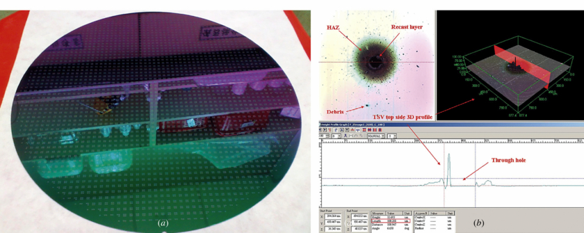
Figure 1. (a) Optical photograph of a laser-drilled wafer. (b) CM photograph of a laser-drilled TSV.
Download figure:
Standard image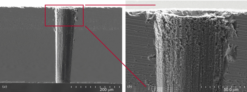
Figure 2. SEM photographs showing (a) full-scale and (b) surface cross-sectional morphologies of a laser-drilled TSV with 40 ns pulses at a repetition rate of 100 kHz.
Download figure:
Standard image3.2. Optimization of WCE etchant
The chemical etchants used in this study were optimized to remove surface and sidewall damage caused by UV ns laser pulses. Figures 3(a)–(c) show the conditions of sidewalls etched with etchants A, B and C, respectively. The sidewall etched by etchant A is clearly smoother than those etched by etchants B and C because only etchant A can finely remove the recast layer. Thus, A is the optimum etchant to satisfy the target condition of smooth sidewalls. Moreover, an appropriate mixture ratio is crucial for TSV WCE, that is, the chemical mixture ratio and process parameters of etchant A must be optimized. The etchant solution A, which consists of a mixture of 49% HF, 70% HNO3 and 100% H2O (diluent), was optimized through the Taguchi robust design method. Subsequently, the optimized solution was used to map its WCE properties to remove the recast layer formed by UV ns laser pulses and provide high TSV quality, where the TSV roundness and lateral etching value were used as the quality targets for the Taguchi experiments. In optimizing WCE etchant A, the criterion for TSV roundness was 'nominal is best' and that for the lateral etching value was 'higher is better'. A TSV roundness with a specific target value of 1 and a larger lateral etching value are indications of better performance. After identifying the most influential parameters, the optimized mixture ratio of etchant A (49% HF, 70% HNO3 and 100% H2O) is 15:9:2. Figure 4(a) shows that although the recast layer and debris are removed, the TSV sidewall remains rough before optimizing the WCE etchant. In contrast, after optimization, a TSV with smooth sidewalls was obtained, without debris on the drilling surface or a recast layer around the hole (figure 4(b)).
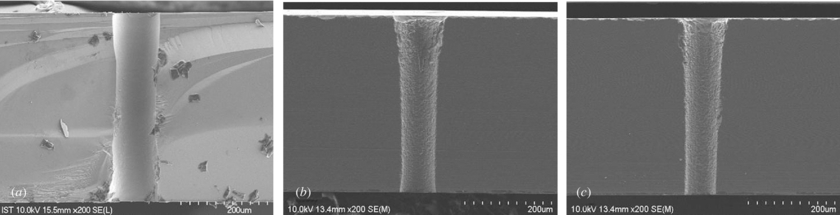
Figure 3. SEM photographs of a laser-drilled TSV sidewall etched for 40 s in (a) HF:HNO3:H2O, (b) HF:HNO3:CH3COOH and (c) HF:HNO3:NH4F as etchants.
Download figure:
Standard image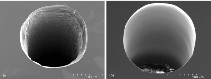
Figure 4. SEM photographs of a laser-drilled TSV sidewall etched for 40 s in (a) HF:HNO3:H2O = 12:3:3 etchant before the mixture ratio was optimized and (b) HF:HNO3:H2O = 15:9:2 etchant after it was optimized.
Download figure:
Standard image3.3. WCE process for HAZ, recast layer and debris removal with a HF, HNO3 and H2O etchant
In this work, we developed a WCE process to eliminate the damage to the wafer surface and TSV sidewall induced by the UV ns laser pulses and thus to obtain superior surface quality. We predict that the proposed method will enable semiconductor manufacturers to use ns laser drilling for industrial WL TSV fabrication because they can achieve the desired sidewall quality and circular TSV shape by incorporating a WCE process suitable for mass production. This prediction is based on three characteristic features of the method. Firstly, isotropic WCE of silicon with HF–HNO3 mixtures is a widely used process in the semiconductor manufacturing industry because it removes work damage and effectively reduces roughness. In TSV applications as well, we predict that TSV sidewall damage will be removed and smooth sidewalls obtained if the surface tension of the WCE etchant is sufficiently small. Secondly, H2O can be used as a diluent to control the etching rate and selectivity of the WCE etchant. We predict that the debris and recast layer formed by UV ns laser pulses will be removed rapidly owing to the unique etching selectivity of WCE. Finally, if a TSV has already been created, the WCE process can simply modify it to a circular shape via an isotropic etching mechanism.
As is evident from the results shown in figures 5(a) and (b), the HAZ, recast layer and debris that formed around a fabricated WL TSV were effectively eliminated through the optimized WCE process. Figures 6(a) and (b) show detailed SEM photographs of full and surface cross-sectional views, respectively, of a TSV after WCE. An approximately 88° taper angle and scallop-free (less than 10 nm) sidewall were obtained without a recast layer after 40 s of etching in a HF:HNO3:H2O etchant. The entrance diameter of the TSV fabricated by the UV ns pulsed laser was approximately 100 µm on average. After WCE processing, this was extended to approximately 150 µm on average. We repeated the WCE experiments with identical or similar compositions (HF:HNO3:H2O = 15:9:2) and demonstrated that variations in the taper angle and TSV diameter were within 10%.
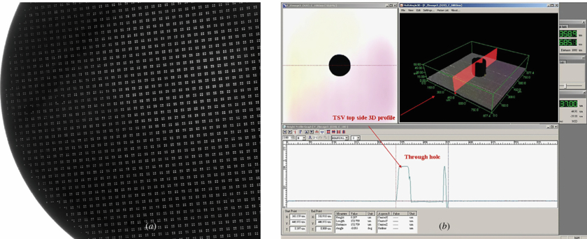
Figure 5. (a) Optical photograph of a laser-drilled wafer. (b) CM photograph of a TSV fabricated by the proposed approach.
Download figure:
Standard image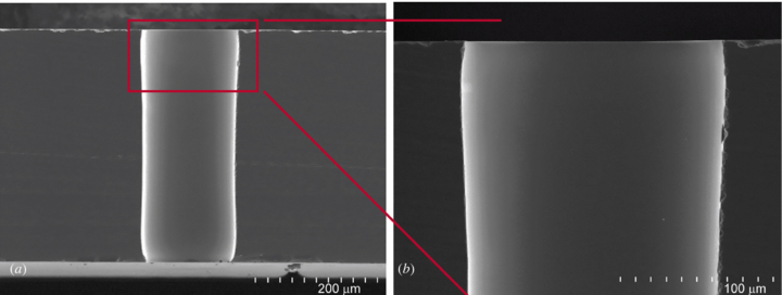
Figure 6. SEM photographs showing (a) full-scale and (b) surface cross-sectional morphologies of a laser-drilled TSV etched for 40 s in HF:HNO3:H2O = 15:9:2 etchant.
Download figure:
Standard imageIn this way, we introduced a simplified process for achieving TSVs of excellent quality with a diameter near 150 µm and an 88° taper angle on a 400 µm thick wafer. However, WCE increases the diameter of the laser-drilled TSV; moreover, there is a physical limit to the aspect ratio by using a UV ns laser drilling technique. Therefore, TSVs with a diameter of less than 100 µm and a depth of 400 µm will be difficult to fabricate with the proposed TSV formation approach. This issue may severely limit its use in advanced TSV applications such as 3D IC and SIP technologies. In further studies, the use of laser drilling with the percussion method for TSV fabrication could be investigated to achieve a TSV diameter of less than 50 µm; that is how the TSVs with a diameter ranging from 50 to 100 µm can be found. In addition, if it becomes possible to use wafers with a thickness of less than 400 µm, the proposed approach may be able to achieve TSVs with a diameter ranging from 50 to 100 µm.
3.4. Comparison of the proposed TSV formation approach and the Bosch DRIE method
With respect to TSV sidewall quality, figure 7(a) shows 10 nm scallops on a sidewall fabricated by the Bosch DRIE process [32]. Figure 7(b) shows that the proposed TSV formation approach can indeed be used to achieve a scallop-free sidewall superior to that obtained by Bosch DRIE.
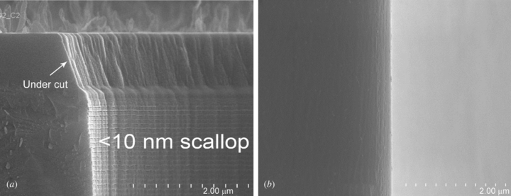
Figure 7. SEM photographs showing (a) 10 nm scalloped profile of TSV fabricated by Bosch DRIE and (b) scallop-free profile and sidewall roughness of TSV fabricated by the proposed approach.
Download figure:
Standard imageRegarding TSV throughput, the laser drilling speed is 8.04 TSVs s–1 on a 400 µm thick silicon wafer and the WCE process time is 40 s. According to published literature on Bosch DRIE, the sidewall roughness can typically be reduced to 10 nm with a maximum etching rate of approximately 4 µm min−1 (i.e. 6000 s for an etching depth of 400 µm) [13–18]. This relationship between processing time and the number of TSVs on a single wafer is plotted in figure 8. Based on 400 µm deep TSV etching with 10 nm sidewall quality and a TSV diameter of 150 µm, the processing speed of the proposed approach is 370% faster than that of the Bosch DRIE process, which corresponds to the etching of 10 000 TSVs on a single wafer for WLP. That is, the proposed approach is more efficient than the Bosch DRIE process as long as the number of TSVs on a single wafer is less than 47 918.
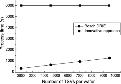
Figure 8. Comparison of drilling time between the proposed approach and Bosch DRIE as a function of the number of TSVs per wafer (TSV diameter = 150 µm).
Download figure:
Standard imageExperimental results demonstrate that the recast layer, debris and rough sidewalls formed by the DPSS UV ns pulsed laser are effectively eliminated by implementing the combined process approach. A summary of the novel approach is shown in figure 9. This process is successfully applied to fabricate TSV for WLP applications.
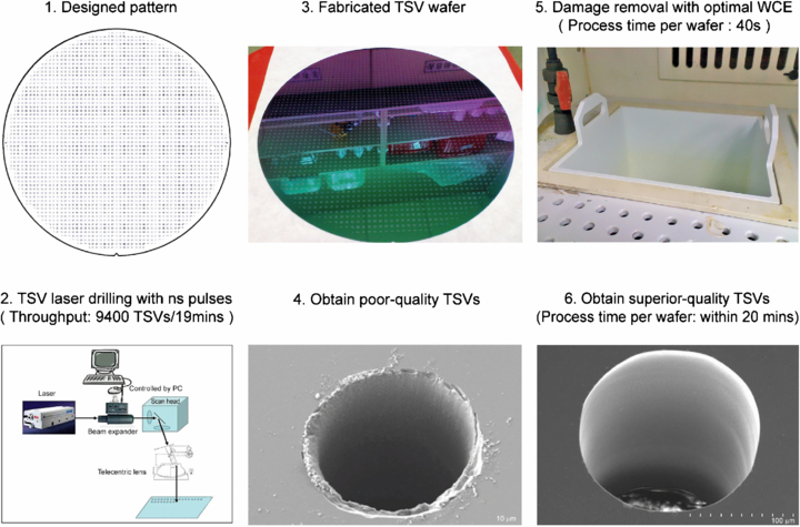
Figure 9. Process flow of the proposed approach for fabricating WL TSVs.
Download figure:
Standard imageConcerning the equipment costs of the proposed TSV formation approach, the DPSS UV laser used in this experiment is approximately US$ 500 000 [33]; the fabrication cost of the WCE tank is approximately US$ 100; and the process cost of WCE for one batch of experiments is approximately US$ 50. Clearly, the proposed approach has a prospective advantage in terms of the cost of process ownership over Bosch DRIE (normally above US$ 1500 000, e.g. for SPTS Bosch DRIE equipment with corresponding lithography equipment [34]). This satisfies the exact requirements for industrial production.
The proposed TSV formation approach is superior to Bosch DRIE owing to its advantages of better TSV sidewall quality, higher TSV throughput, and lower cost of ownership.
4. Conclusions
This study, in demonstrating an innovative WL TSV formation approach that integrates a DPSS UV ns pulsed laser and a rapid WCE process, constitutes an important step toward the mass production of WLP technology. In terms of drilling efficiency, for 10 000 TSVs with a diameter of 150 µm and a depth of 400 µm, the proposed approach represents an improvement of 370% over Bosch DRIE. Regarding TSV quality, the sidewall roughness with the proposed approach was greatly reduced to less than 10 nm (scallop-free) by rough laser drilling and rapid WCE, making it superior to that with Bosch DRIE (10 nm). As for the cost of module ownership, which is the overriding concern in industrial production, the proposed approach has a significant advantage over Bosch DRIE. In sum, the proposed approach outperforms the conventional Bosch DRIE process in three critical respects, as demonstrated in this study for the case of an LED sub-mount. Hence, we conclude that our approach for manufacturing WL TSVs can contribute significantly to the semiconductor industry.
Acknowledgments
The authors are grateful to Dr Mike Yang, Mr Stephen Liao, and Mr Thomas Huang of the Phoenix Silicon International Corporation (PSI), Taiwan, for their support as well as their advice on WCE. The authors also thank Mr Jefferson Lin of Marketech International Corporation (MIC), Taiwan, for his technical assistance in laser drilling.