

Abstract
Patterns formed by the laser direct writing (LDW) lithography process are used either as channels or barriers for MoS2 transistors fabricated via inkjet printing. Silver (Ag) nanoparticle ink is printed over patterns formed on top of the MoS2 flakes in order to construct high-resolution source/drain (S/D) electrodes. When positive photoresist is used, the produced grooves are filled with inkjetted Ag ink by capillary forces. On the other hand, in the case of negative photoresist, convex barrier-like patterns are written on the MoS2 flakes and patterns, dividing the printed Ag ink into the S/D electrodes by self-alignment. LDW lithography combined with inkjet printing is applied to MoS2 thin-film transistors that exhibit moderate electrical performance such as mobility and subthreshold swing. However, especially in the linear operation regime, their features are limited by the contact effect. The Y-function method can exclude the contact effect and allow proper evaluation of the maximum available mobility and contact resistance. The presented fabrication methods may facilitate the development of cost-effective fabrication processes.
Export citation and abstract BibTeX RIS
1. Introduction
Laser direct writing (LDW) lithography in resists may enable simplification of the process at a reduced cost; the desired structures and patterns are directly built without requiring vacuum conditions and the use of masks. For these reasons, LDW techniques can be utilized in a wide range of applications for the fabrication of passive electronic components and interconnections, and even in tissue engineering and array-based biosensors [1]. In particular, not only for high DC performance, but also for high AC performance, the channel length of thin-film transistors (TFTs) is a critical parameter of the cut-off frequency. Various techniques have been adopted for making short channel devices, in particular sub-micron sized devices.
Regarding the production of the finer features, e-beam, focused ion beam, and deep ultraviolet/x-ray exposure are considered as attractive methods. These techniques allow site-specific nano-machining to unprecedented levels of precision and accuracy. Confinement of the optical energy to small dimensions can be achieved by coupling laser irradiation to near-field scanning optical microscopes [2]. In addition, through ultrafast laser (e.g. femtosecond laser) radiation that drives non-linear or multiple-photon absorption in nominally transparent materials such as glass and polymers, 3D stereo-lithographical structures can be formed with nano-scale feature size [3]. Aside from feature resolution, important challenges of the aforementioned approaches are scalability, throughput, and high cost due to complicated equipment hardware.
To further increase productivity, reduce the fabrication cost, and simplify the fabrication process, drop-on-demand inkjet printing has been widely used in ultra-low-cost, low-temperature, and large-area electronics such as TFTs, radio-frequency identification tags, microelectromechanical systems, and sensor applications [4–8]. Here, we note that, for making printed devices, inkjet, screen, roll-to-roll including flexography, off-set, and gravure processes are the most encountered printing technologies, depending on the dimensional or geometrical considerations of the target surfaces, and fluidic and the wetting characteristics of the inks. Among the printing methods, inkjet printing is the most versatile since it is compatible with a variety of substrates and materials and can also print on shaped objects. Although inkjet printed TFTs have shown enhanced electrical characteristics in recent years [9–11], further improvement is still needed with respect to power-consumption, high electrical characteristics, and printing resolution. For example, although the maskless and non-contact inkjet printing process can be easily adapted to the organic and oxide based TFT fabrication process, the printed TFTs still show relatively poor electrical performance and environmental stability [9, 12–14]. Inkjet printing is also not suitable for applications requiring high-resolution due to the limitation of the printing-nozzle size, which results in relatively large minimum feature size (millimeter or several hundred micro scale). Moreover, the edge waviness of inkjet printed source/drain (S/D) electrodes on short-channel TFTs can affect the ID uniformity [15]. To address these issues, novel semiconducting materials and printing techniques are required for high-performance integrated electronics.
In this paper, atomic layered 2D MoS2 is selected as a promising alternative channel material due to its exotic electrical, optical, and mechanical properties. 2D MoS2 has n-type semiconducting characteristics with a relatively large band gap (direct (1.8 eV) or indirect band gap (1.2 eV) depending on the exact number of atomic layers) compared to zero-gap graphene [16–19]. In addition to the interesting band structure, 2D MoS2 shows attractive characteristics for switching devices: high carrier mobility (∼200 cm2 V−1 s−1 range at high-k hafnium oxide (HfO2) and room temperature), high on/off current ratio (Ion/Ioff, ∼106), low subthreshold swing (SS) (∼70 mV per decade), and an absence of dangling bonds [16, 20, 21]. Furthermore, MoS2 of very thin atomic thickness (6.5 Å) has good mechanical flexibility.
For creating well-defined high-resolution electrodes, LDW, in conjunction with liquid phase Ag inkjet printing, are employed. Capillarity and self-alignment help realize a 2D MoS2 transistor with a sub-2 μm channel. The electrical conductivity of Ag is the highest of all metals (∼6.3 × 10⁷ S m−1 at 20 °C) [22, 23]. Nanoparticle Ag ink suspensions require lower sintering temperature (below 150 °C) compared with Au or Cu (∼250 °C) to realize high conductivity [24, 25]. The relatively low work function (4.3 eV) of Ag is suitable for electrodes of n-type semiconductor materials minimizing the barrier between the semiconductor and S/D electrodes. The highly crystalline MoS2 semiconductors, combined with the S/D electrodes made of sintered Ag inks lead to fabrication of transistors having sub-2 μm channel length exhibiting moderate switching behavior. These results indicate that LDW lithography and inkjet printing technologies can have potential applications in future flexible/wearable electronics, facilitating cost-effective fabrication processes.
2. Results and discussion
2.1. Line-by-line laser scanning
A basic configuration of single line-by-line laser processing is accomplished by implementing a precision translation system on a single platform, as shown in figure 1(a). We use an infinity corrected high magnification objective lens (Mitutoyo, numerical aperture = 0.5, focal length = 2 mm, and magnification = 100×) to create fine patterns (of ∼2.0 μm width) as well as to observe in situ via a camera. Note that in order to overcome serial direct writing by a single probe, a probe array scheme utilizing a digital mirror display array and piezo-scanners has been developed for increased throughput [26]. A positive photoresist (Fujifilm, OiR-906-12, i-line), which is dissolved within the illuminated area during development, is applied as a photo-sensitive material. We also test and apply the negative photoresist (SU-8 2002, MicroChem), whose non-illuminated area dissolved. Three representative feature trends are observed: the width, height, and even the profile of the resists vary, depending on the laser power and scan speed of the stage (i.e. exposure time). The departures are because the Gaussian beam profile of the laser scales with the peak intensity (see online supplementary figure S1 for detail). Note that the laser-scanned area has a crater shape in the case of positive photoresist, while the behavior of negative photoresist is the opposite (i.e. the laser-scanned area is embossed) as shown in figures 1(b) and (c).

Figure 1. (a) Schematic view of the optical setup for LDW lithography and representative optical microscope images, (b) for positive photoresist and (c) for negative photoresist after the LDW lithography and development.
Download figure:
Standard image High-resolution image2.2. Inkjet printing process
2.2.1. Capillary with positively laser-patterned geometry
Grooves are generated by using LDW lithography and positive photoresist. The fabricated patterns are filled with inkjetted Ag ink (CCI-300, Cabot Corp., material properties in online supplementary table S1) to form the S/D electrodes. Capillarity is the driving force for the filling process (figure 2(a)), which exhibits distinct variations, as depicted in figures 2(b)–(d). Therefore, we need to understand the relationship between capillarity and the geometry of the channel. As the patterned channel is open at the top, the capillary pressure is given by [27, 28]:
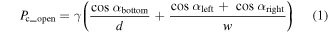
where γ is the surface tension of the filled liquid, α is the contact angle of the liquid, d is the depth of a channel, and w is the width. The volume flow rate (Q) is expressed in open channels [27, 28] by:

where η is the viscosity of the ink, ΔP is the pressure difference across the ink front and the ambient air, and Rf is the flow resistance. Because of the complexity of the velocity profile in rectangular ducts, an approximate solution can be constructed through a Fourier series expression. By retaining six terms, the deviation of this prediction from the exact solution is within ∼0.05%. Thus, Rf is given by [27, 28]:
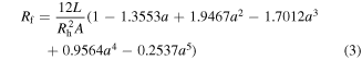
where L is the filled length of channel and A is the cross-sectional area of the channel. Rh is the hydraulic radius of the channel and defined as Rh = 2A/P (P is the wetted perimeter of the cross-section). Moreover, a is the aspect ratio defined as height (h)/width (w) (if h ≤ w) within the range (0 ≤ a ≤ 1).

Figure 2. (a) The top-view of a confocal laser microscope image of line patterns of positive photoresist and partially filled Ag ink by capillary forces after the process of LDW and inkjet printing of Ag ink. (b)–(d) The top-view images of line patterns with varying widths of the channel using positive photoresist and filled Ag ink after the process of LDW and inkjet printing. The thicknesses of the spin-coated photoresist are the same (∼1.0 μm), however, the widths are different: (b) 2.0 μm, (c) 4.0 μm, (d) 15.0 μm.
Download figure:
Standard image High-resolution imageTo boost the capillary flow, Q, ΔP should be increased (equation (2)) via reducing w (equation (1)). We note that increasing h is subject to limitations since the thickness of the resist is regulated by the speed of a spin coater and the physicochemical properties of the photoresist, especially the viscosity. Photoresist of ∼1.0 μm thickness is formed by spin coating at 2000 rpm. When a lower speed is used to form a thicker channel, the thickness uniformity worsens. Figures 2(b)–(d) show that decreasing w < 2.0 μm strengthens the capillary force and flow. A similar trend is observed in an additional experiment using a channel with continuously broadening width (online supplementary figure S2). Most of the capillary force and flow into the channel develop in the initial stages, and then diminish due to the increasing Rf (equation (3)) that balances the capillary force. An experiment aiming at filling adjacent channels with Ag ink, separated by variable distance, is also carried out (online supplementary figure S3). After the inkjet printing, the filled ink is sintered at 180 °C for 30 min at a hot plate for improving electrical conductivity and connections.
2.2.2. Self-alignment through negatively laser-patterned geometry
Based on the aforementioned conditions (laser power of 5.0 μW and scan speed of 5 μm s−1 in (section 2.1) irradiated on resist spin coated at 3000 rpm for 60 s) a barrier of ∼2.0 μm thickness is built as shown in figure 3(a). Ag ink is then printed across the barrier as shown in figure 3(b). The jetted Ag ink line breaks since the wall height (∼2.0 μm) exceeds the printed ink thickness (∼430 nm). The ensuing sintering process (at 180 °C for 30 min at a hot plate) further facilitates the Ag line breakup (figure 3(b)) as the differential thermal expansion and the ink shrinkage weaken the line structure. We note that thermal expansion coefficients of Ag and SU-8 are 19.68 ppm °C−1 and 52.0 ppm °C−1, respectively.
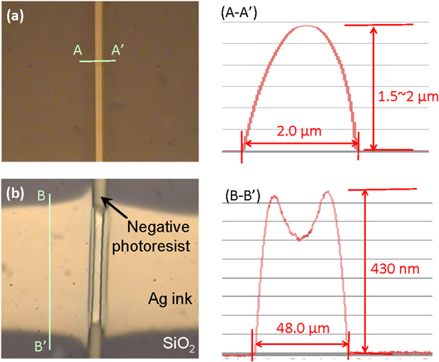
Figure 3. The top-view images and cross-sectional profiles measured using a 3D confocal laser microscope for (a) the negatively patterned wall and (b) magnified image for printed Ag ink over the walls after inkjet printing of Ag ink. The measured profiles are of exaggerated scale in order to improve the shape clarity.
Download figure:
Standard image High-resolution image2.3. MoS2 transistors
Through the laser-induced fine patterns (using either positive or negative photoresists) in combination with inkjet printing, multilayered MoS2 transistors are fabricated. During the LDW process, the irradiated laser does not damage MoS2 because the applied laser power (5 μW) is very small compared to the ablation threshold of MoS2 (online supplementary figure S4). The capillarity induced flow for the positive photoresist and the self-alignment for the negative photoresist allow the one-step formation of the S/D electrodes, as shown in online supplementary figures S4(a) and (b); figures 4(a) and (b) show the representative MoS2 TFTs fabricated by these procedures. The electrical characteristics of the fabricated devices are examined. The log- (left) and the linear-scale (right) ID–VG curves of the representative MoS2 TFT with the S/D electrode formed by capillarity driven filling (VD = 0.1 V in (figure 5(a)) are plotted. The device has a channel length of 2 μm and a width of 4 μm. Note that the thickness of the MoS2 flake is around 55 nm. At room temperature and in air, the as-fabricated MoS2 TFT exhibits acceptable switching behavior (Ion/Ioff of ∼104), an SS of ∼2.54 V/decade, a linear field effect mobility (μeff_lin) of ∼2.87 cm2 V−1 s−1, typical n-type behavior with negative threshold voltage (VTH), and a normally ON-state for the device at low VD (= 0.1 V). As shown in figure 5(b), the ID–VD in a range from 0 to 8 V for the selected VG (from −20 to +20 V in 10 V increments) is plotted. In the inset of figure 5(b), a non-linear output curve in a very low VD regime (from 0 to 2.0 V) is observed due to the Schottky barrier (ΦB) between the MoS2 and inkjet printed Ag electrodes. MoS2 TFTs with a channel length of 2 μm and width of 2 μm are also fabricated by the self-alignment method. In figure 6, the electrical performance of representative device exhibits similar characteristics to the previously examined device. At low VD (= 0.1 V), Ion/Ioff of ∼103 and an SS of ∼3.72 V/decade are obtained and μeff_lin of ∼10.18 cm2 V−1 s−1 is extracted by the MOSFET square-law model (figure 6(a)). Moreover, from the ID–VD in figure 6(b), non-linear output characteristics are again observed (see also figure 6(b)).
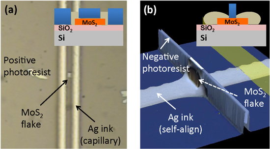
Figure 4. The optical images of fabricated MoS2 TFTs, (a) using the positive photoresist and capillary (note that the representative device has a channel length of 2 μm and a width of 4 μm), and (b) using the negative photoresist and self-alignment with inkjet printed Ag ink (note that channel length and width are 2 μm and 2 μm, respectively).
Download figure:
Standard image High-resolution image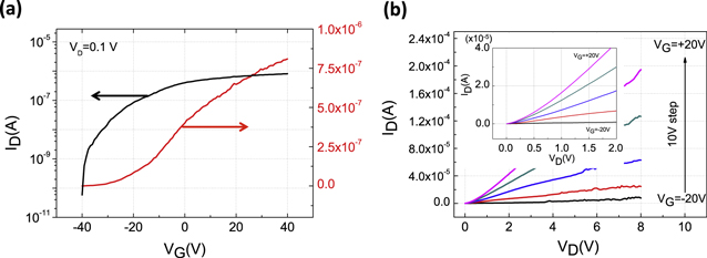
Figure 5. Device performances of MoS2 TFTs with Ag electrodes formed by capillary and positively patterned channels. (a) Transfer characteristics (ID–VG) for the representative MoS2 transistor in log-scale (left) and linear-scale (right) at VD = 0.1 V. (b) Output characteristics (ID–VD) in the range of VD from 0 V to 8 V with 10 V step of VG (from −20 V to 20 V). Inset: magnifications for the low VD range from 0 to 2.0 V.
Download figure:
Standard image High-resolution image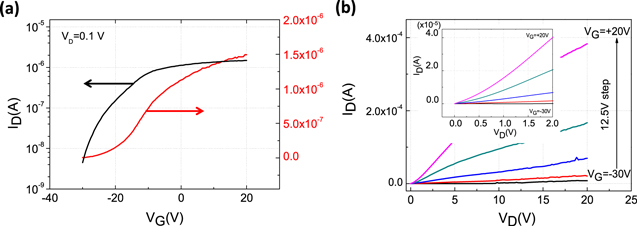
Figure 6. Device performances of MoS2 TFTs with the Ag electrodes formed by self-alignment and negatively patterned walls. (a) Transfer characteristics (ID–VG) for the representative MoS2 transistor in log-scale (left) and linear-scale (right) at VD = 0.1 V. (b) Output characteristics (ID–VD) in the range of VD from 0 V to 20 V with 12.5 V step of VG (from −30 V to 20 V). Inset: magnifications for the low VD range from 0 to 2.0 V.
Download figure:
Standard image High-resolution image
MoS2 TFTs could have large variation in their performances, depending on the structure, process quality, and uncertainty of the geometry of MoS2 flakes caused by the nature of exfoliation; our extracted μeff of both devices is comparable with the low-end of existing vacuum-processed devices (the range: 0.2 to 14 cm2 V−1 s−1), however, μeff is relatively lower than other vacuum-processed MoS2 TFTs (the range: 30 to 60 cm2 V−1 s−1), as shown in online supplementary table S2. One of the possibilities of changing the electrical behavior is the ΦB or large contact resistance (Rc) [29–31]. The plots in figures 5(b) and 6(b) confirm that the ΦB is formed at the contact between the inkjetted Ag electrodes (as a metal) and the MoS2 flakes (as a semiconductor). Furthermore, the solution-based ink could make an unintended interfacial layer and barrier at the contact due to gas pockets, fully uncapped particles, oxidized particles, or undissolved materials [32]. The undesirable contacts can conceal the inherent performance of the devices. Therefore, to estimate the potential properly, we need to exclude the contact effect. Y-function method (YFM) helps us extract the maximum available mobility (μ0) and Rc in the device [33–37]. Through the YFM, the extracted μ0 at a low VD of 0.1 V are 8.91 cm2 V−1 s−1 (improved from 2.87 cm2 V−1 s−1, 67.77%) for the device fabricated by capillary force and 22.71 cm2 V−1 s−1 (improved from 10.18 cm2 V−1 s−1, 55.17%) for the device formed by self-alignment (figures online supplementary S5(a) and (b)). These considerable discrepancies between μeff_lin and μ0 originate from the contact effect because the extracted μ0 is not affected by the contact factor. Also, on the ID–VD curves, the non-linear trends arising from the contact barriers are presented clearly at low VD (figures 5(b) and 6(b)). To further investigate the contact effect, in figure online supplementary S5(c), the mobility attenuator factor (θ = θ0 (the channel interface) +θ* (the contact)) is considered and through the extracted θ, the maximum value of Rc (Rc_max) can be obtained when we assume that the effect of θ0 is very small (≈0). Note that the calculated values of Rc_max are 82.3 kΩ (for capillary) and 64.7 kΩ (for self-alignment). The values of Rc_max are 2–3 times larger than well-designed other devices: 17.0 kΩ [21], 27 kΩ [16], 23.4 kΩ [38], 28.9 kΩ [31]. This is because (1) nanoparticle based inks yield reduced properties in comparison with their bulk counterparts (e.g. conductivity: ∼70% of bulk), (2) a thermally sintered Ag electrode shows a somewhat higher work function (4.27–4.72 eV depending on the sintering temperature) compared with that of a vacuum-deposited Ag (4.2 eV), which we expected [39], (3) a slightly oxidized surface causes unintended contact properties [32]. Furthermore, Rc_max (82.3 kΩ) formed by capillary forces is larger than Rc_max (64.7 kΩ) produced by self-alignment because the self-aligned Ag electrodes are much wider (∼50 μm) and have a larger injecting electrode area (more than 10 times) than the electrodes created by capillarity. Also, the dominant contact resistance contributes to the mobility, especially the linear mobility; μeff_lin (∼10.18 cm2 V−1 s−1, for self-alignment) is much higher than μeff_lin (∼2.87 cm2 V−1 s−1) of the device with the electrodes formed by capillarity. In addition, it should be noted that interface quality is also an important factor affecting the electrical performance of the devices [29, 40]. Through high-k insulators (e.g. HfO, Al2O3, ZrO2, PMMA) phonon scattering can be suppressed and the interface quality can be improved [21, 40–42]. For the aforementioned reasons, MoS2 TFTs with inkjet printed Ag electrodes exhibit lower electrical performance compared to previous MoS2 TFTs fabricated by conventional vacuum processes and well-designed contacts [16, 21, 29–31, 38]. Despite its shortcomings, the printing process still draws strong attention because of potentially low cost, low process temperature, compatibility with flexible substrates, and ability to deposit unique features. Moreover, the printing process performance has improved steadily with the development of printable materials.
3. Conclusions
In summary, laser-induced fine patterns were built using positive and negative photoresists. Depending on the type of the photoresist, grooves or convex barriers were written on demand in positive and negative resists, respectively. The formed patterns effectively guided the fabrication of the S/D electrodes upon deposition of Ag inks.
Through the laser writing of fine patterns and inkjet printing, MoS2 TFTs were fabricated. The as-fabricated devices exhibited workable electrical performance in the linear regime. However, the Ag nanoparticle ink formed electrodes presented relatively high electrical resistance and low conductivity compared to the bulk material. Nevertheless, the sub-2 μm length channel demonstration highlights the possibility of combining direct laser lithography and inkjet printing for maskless fabrication of flexible devices based on ultrathin-layered semiconductors.
4. Experimental section
4.1. Profile measurement
The morphologies of printed electrodes formed by capillarity and self-alignment are measured through a 3D confocal laser microscope (Olympus, LEXT OLS4000).
4.2. Sample (MoS2 transistors) preparation
100 nm-thick SiO2 was thermally grown on a heavily doped p-type Si substrate (resistivity < 5 × 10⁻³ Ω cm) as a gate dielectric layer. Then, MoS2 flakes were mechanically transferred from bulk MoS2 crystals (SPI Supplies, USA) on the deposited dielectric layer. After that, the positive (OiR-906-12, Fujifilm) or negative (SU-8 2002, MicroChem) photoresist was formed by a spin coating process at 2000 rpm for the positive photoresist and at 3000 rpm for the negative photoresist. Note that the formed thicknesses of the positive and negative photoresist were ∼1.0 μm and ∼1.5 μm, respectively. The LDW lithography through a pulsed laser (A Spectra Physics, Navigator) with 40 ns pulse duration at 20 kHz, (200 kHz maximum frequency) and 355 nm wavelength allowed the definition of concave patterns (positive) as the channels and convex patterns (negative) as the walls. For the S/D formation, nanoparticle type Ag ink (particle size of ∼70 nm, CCI-300 from Carbot Corp.) filled in a 10 picoliter cartridge having a nozzle size of 21 μm was inkjet printed with a drop spacing of 25 μm and translation speed of 7 m s−1 onto the patterned reservoir and barrier to form the capillary force and self-alignment induced S/D, respectively. After printing at room temperature, thus enhancing the filling and separating of the ink, the S/D was sintered at 180 °C for 30 min on a hot plate under atmospheric environment. All the inkjet printing processes were performed using the DMP 2831 (Dimatix, Fujifilm). After the inkjet printing process, jetted Ag inks were sintered at 180 °C for 30 min in air at a hot plate for reducing the resistance and boosting electrical conductivity.
Acknowledgments
H-J Kwon and C P Grigoropoulos appreciate the support of the U.S. Air Force Office of Scientific Research AFOSR/ AOARD: FA2386-13-4123. for supporting this research. H-J Kwon and S Chung contributed equally to this work.