

Abstract
We present an investigation of contact properties of a germanium (Ge) nanowire based nanoelectromechanical (NEM) switch in its ON state. The contact stiffness in the ON state was evaluated by detecting the nanowire's resonance frequency. It was found that the resonance frequency increases when electric current flows through the nanowire/counter electrode contact area. The reason for modification in the contact area is referred to as electric-current-induced processes in the native oxide layer covering the nanowires. The presented resonance shift method is a simple way to indicate strengthening of the nanowire/counter electrode contact area without disassembling the contact.
Export citation and abstract BibTeX RIS
1. Introduction
Nanoelectromechanical systems (NEMS) are devices that combine mechanical and electrical functionality at the nanoscale level. These systems are the next step in the miniaturization of microelectromechanical systems (MEMS) [1]. The expected benefits of NEMS that could significantly impact wide areas of science and technology are increased efficiency, reduced size, and decreased power consumption [2].
Current examples of NEMS include nanoresonators [3–7] and a range of nanorelays and switches (ON-OFF devices) [8–21], in which carbon nanotubes [9–12, 16, 18, 20], semiconductor [13, 14, 21], metal [15, 19] and organic nanowires [17] have often been used as active components. Ge nanowires are excellent candidates to be used as active elements in NEM switches due to high Young's modulus, ability to withstand high strains, single crystalline nature, and good compositional reproducibility [22, 23]. In ambient conditions, Ge nanowires are covered with a nonconductive native oxide layer. In terms of NEM switch operation, a native oxide layer allows reduction of the 'jump-to-contact' electric current, preventing burnout failure. In addition, the switch can be operated at higher voltages, as reported previously by our group [13, 21].
Active research is being conducted to replace conventional complementary metal-oxide semiconductor (CMOS) devices for specific applications, as well as to improve functioning of CMOS devices by producing hybrid systems [24]. Although both CMOS and NEM technologies are suited for similar applications, such as memory, logic, and transistors [25–27], they differ greatly in operating conditions, working principles, properties, and fabrication. Compared with CMOS switches, the advantages of NEM switches, together with those already listed, also include a near-zero leakage current and potentially higher speed of operation. In addition, NEM switches exhibit stable performance with respect to external conditions such as high temperature [28] and external fields [29].
Although most of electrically controlled NEM switches are configured to use three electrodes [8–10, 19, 20], namely source, drain, and gate, the ON-OFF switching of NEMS can also be achieved in a gateless two-terminal configuration. The advantage of the two-terminal configuration is in its simplicity, where only two electrodes are used. The active element (nanowire) and the counter electrode of an electrostatically actuated two-terminal switch are initially physically separated (OFF state). The operation of an electrostatically actuated NEM switch is performed by balancing electrostatic, adhesion, and elastic forces. Applying voltage between the electrodes of a NEM switch leads to mechanical deformation of the active element and its consequent jump-to-contact with the counter electrode (ON state). Adhesive plus electrostatic forces keep the switch in ON state, while an elastic restoring force brings it to the initial OFF state when the voltage is turned off.
Due to surface forces that are dominating at the nanoscale, NEM switches may suffer from high adhesion in the ON state. One way to overcome the adhesion is to increase the distance between the electrodes to generate larger elastic pull-off force to reverse the state of the switch. With increased electrode separation, higher operational (jump-in) voltages must be used to establish the contact. Switch operation at these voltages may lead to mechanical breakdown [25], melting, and burnout of the active element [13, 15, 30]. Semiconductor [31] and metallic [32] nanowire welding in nanosized contacts has been reported. To ensure stable operation of the switch, it is essential to know how the electrical and mechanical properties of contact change with respect to applied voltage and electric current flow through the contact.
This research is focused on investigation of the contact-strengthening phenomenon that takes place during the nanowire operation in the ON state. We evaluate modification of the nanowire/counter electrode contact area induced by electric current flow through the contact. The method implies in situ detection of shift of the resonance frequency of Ge-nanowire-based NEM switch in the ON position. It allows choosing the proper device architecture and voltage values for stable NEM switch operation.
2. Methods
Ge nanowires used in the NEM switches as active elements were grown using the supercritical fluid method [33]. The structure of nanowires was determined by FEI TECNAI TEM. For obtaining cantilevered active elements, the nanowires were suspended on a TEM grid pre-coated with 5 nm chrome and a 20 nm gold layer (Gatan 682 PECS) and clamped with platinum strips (figures 1(a)–(b)) using e-beam deposition technique (SEM-FIB TECNAI LYRA). The widths of the platinum strips were at least five times larger than the nanowire diameters (figure 1(b) inset) in order to obtain a 'fixed' end of the cantilevered nanowire (the width of the strip must be at least the size of the diameter of the nanowire) [34]. Argon etching (Gatan 682 PECS) was performed for partial removal of native Ge oxide outer shell, formed under ambient conditions.
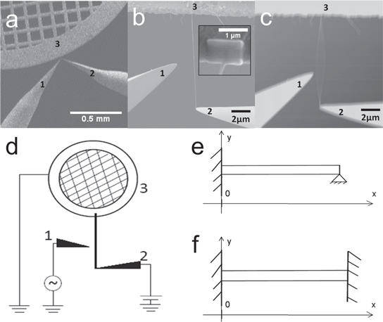
Figure 1. (a) Overview of experimental setup in situ SEM; (b) close up of NEM switch (inset—platinum strip for nanowire clamping); (c) Ge nanowire in resonance state; (d) schematics of system; (e) schematics of 'fixed-pinned' boundary conditions; (f) schematics of 'fixed-fixed' boundary conditions.
Download figure:
Standard image High-resolution imageThe measurements were carried out in situ using a SmarAct 13D nanomanipulation system staged inside a field emission scanning electron microscope Hitachi S-4800. Electrochemically etched gold tips were used as electrodes. Nanowire oscillations were excited electrostatically by applying ac voltage between electrode 1 and grounded electrodes 2 and 3 (figures 1(a)–(d)). The behavior of the nanowire during the ac signal sweep was visualized in real-time SEM TV regime. Nanowire resonance was detected as a sharp increase of oscillation amplitude (figure 1(c)).
For the oscillation excitation in the nanowires, signal generator Agilent N9310A was used. Source-meter Keithley 6430 was used for voltage application and electric current measurements.
3. Results and discussion
From a mechanical standpoint, we can model the NEM switch in the ON state as a double-clamped beam resonator (figures 1(b), (c), (e) (f)). Assuming the nanowire in an NEM switch ON state can be described using the Euler–Bernoulli theory for an elastic beam, and solving the general Euler–Lagrange equation  [35], where E is the Young's modulus, I is the moment of inertia, and μ is the linear density of beam, an expression for the resonance frequency is obtained from equation:
 [35], where S is a cross sectional area of a nanowire (circle), ρ is density of the nanowire, and β is an eigenvalue parameter that depends on the boundary conditions and on the oscillation mode of the nanowire. In our experiment, the clamped end of the nanowire (figures 1(e), (f) electrode 3) can be described by the 'fixed' boundary condition:
 [35], where y is the displacement of the nanowire and x is the coordinate along the axis of the nanowire starting from the fixed end of the nanowire.
Initially, the nanowire was brought in contact with the switch electrode without any voltage applied between the electrodes. This state could approximately be described by the 'pinned' boundary condition  [35], where L is the length of the nanowire. It was expected that the switch contact (figure 1(b)) could strengthen after the voltage was applied between the NEM electrodes, thus shifting the boundary condition describing the switch contact from 'pinned' toward 'fixed,' i.e.
  [35].
[35].
Eigenvalues βfixed-fixed = 4.730 04 for a 'fixed-fixed' beam and βfixed-pinned = 3.9266 [35] for a 'fixed-pinned' beam of the first oscillation mode were obtained from boundary conditions described previously. The eigenvalue for a single-clamped nanowire is 1.875 [35]. The frequency ratio of 'fixed-fixed' and 'fixed-pinned' resonances  is 1.45. This means that, if the contact strengthening happened, the resonance frequency of the nanowire could increase for not more than 45% from its initial value. It should be noted that for the actual experimental switch, contact strengthening may not reach the 'fixed' state as well as the initial state could not be 'pinned.' In both circumstances, the actual frequency change would not exceed 45%.
In the case of electrical excitation, the force F acting on the nanowire is in the form of 
 +
+  +
+  where B is a proportional constant, Q0 is a charge that balances the potential difference caused by different surface work functions of the Ge nanowire and the gold electrode, α is a geometrical factor, VAC is the amplitude of applied voltage, ω is the angular frequency of the electric field, and t is time [36, 37]. Thus, for the nanowire with natural frequency f, the resonance will occur when the driving frequency is f and f/2.
As the nanowire single-clamped resonance frequency was easier to determine than the double-clamped resonance frequency, before each experiment, both resonances for single-clamped nanowire occurring at the ac driving frequencies f and f/2 were determined. Typical true amplitude-driving frequency characteristics have a symmetrical curve (figure 2), where the maximum amplitude indicates the resonance frequency.
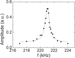
Figure 2. True amplitude-driving frequency characteristics for a single-clamped nanowire of length and radius of 18 μm and 80 nm respectively, with Lorentzian fit (line).
Download figure:
Standard image High-resolution imageWhen the single-clamped resonance frequency was determined, the cantilevered nanowire was brought in contact with the switch electrode (figures 1(a)–(d) electrode 2) to form a switch contact in the ON state (figures 1(b), (d)). Based on the determined single-clamped resonance frequency and the boundary conditions discussed previously, the resonance frequency was searched in expected frequency range fdouble (4.39;6.36)·fsingle and measured accordingly. For control, for some nanowire resonance at excitation frequency f/2 was also determined.
To determine contact properties, the ac voltage amplitude was set to 0 V and the dc voltage was swept between the electrodes 2 and 3, from 0 V to the desired voltage U' and back to 0 V (figures 1(b), (d)). After each dc voltage sweep, the resonance frequency of the double-clamped nanowire f was again measured. This cycle, consisting of a dc voltage sweep and a resonance measurement, was repeated with increasing voltage U', until one of the safety limitations was reached (i.e., a predefined electric current saturation of 10 nA or I(V) cycling amplitude of 30 V), which were introduced to avoid the potential damage of the nanowire, as reported in previous research [13, 15, 30, 38].
Figure 3 shows the relative change of the resonance frequency of a Ge nanowire covered with a native oxide layer and current density in the contact area versus voltage applied to the nanowire. The predetermined resonance of the cantilevered single-clamped nanowire was 145 kHz. According to the eigenvalue ratios, the resonance frequencies of 'fixed-pinned' and 'fixed-fixed' beam configurations should have been 636 and 923 kHz, respectively. Initially measured resonance frequency f0 of the double-clamped nanowire was 660 kHz, which means that the contact properties are close to the 'fixed-pinned' conditions. It can be seen that when applied U' is below 9 V and the current density in the contact is small (figure 3 inset), the resonance frequency of the nanowire slightly changes. For the values of U' between 9 and 15 V, which coincide with a noticeable increase of current density j (the contact areas for current density calculations were obtained using Carpick's generalized equation [13, 15, 23, 39, 40]), a rapid increase in the resonance frequency was observed, indicating strengthening of the switch contact. Although j increases further, the rapid change of the resonance frequency (34% increase) was followed by its stabilization (fmax = 884kHz) at voltages above 15 V and current densities above 16 pA nm−2, meaning that in accordance with the mechanical model, the contact had become more rigid.
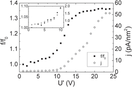
Figure 3. Relative change of the resonance frequency of the nanowire and current density j in the contact area versus voltage U' applied to the nanowire. Inset—the beginning of the graph.
Download figure:
Standard image High-resolution imageThe data relating to maximum frequency increase ratios fmax/f0, current densities jst at the point when frequency stabilizes, estimated Ge nanowire/Au electrode contact areas, and maximal applied voltage U' are summarized in table 1. As it can be seen from the table 1, the current density values jst for all experiments except experiment Nr. 2 are fluctuating within an order of magnitude, which can indicate similar processes in all examined nanowires. The difference in jst values can be attributed to error in contact area parameter estimation from SEM micrographs.
Table 1. Experimental data about maximum frequency increase fmax/f0, estimated Ge nanowire/gold electrode contact area A, stabilization current density jst, and maximum voltage U'.
| exp Nr | wire Nr | fmax/f0 | A·102, nm2 | jst, pA nm−2 | U', V |
|---|---|---|---|---|---|
| 1 | 1 | 1.35 | 2.8 | 11 | 30 |
| 2 | 2 | 1.09 | 27 | 0.24 | 29 |
| 3 | 2 | 1.04 | 19 | 1.0 | 38 |
| 4 | 3 | 1.22 | 1.0 | 11 | 25 |
| 5 | 4a | 1.34 | 2.0 | 16 | 24 |
| 6 | 4a | 1.30 | 5.1 | 14 | 18 |
| 7 | 4a | 1.23 | 0.4 | 3.6 | 17 |
| 8 | 4a | 1.15 | 2.0 | 12 | 16 |
| 9 | 4a | 1.15 | 1.7 | 18 | 25 |
| 10 | 4a | 1.13 | 4.7 | 7.5 | 17 |
| 11 | 4a | 1.15 | 6.3 | 16 | 14 |
aExperiments carried out after Ar ion treatment to achieve different oxide thicknesses.
To analyze electric-current-induced modifications in the contacts, I(V) characteristics were studied (figure 4(a)). From figure 4(a), it can be seen that I(V) characteristics have a 'nonconductive' voltage gap that changes during I(V) cycling. For analysis of the 'nonconductive' gap, associated with the presence of an oxide layer on the surface of the nanowire [13], the value of characteristic voltage U0 was defined as a minimal voltage for which the electric current was not a linear function of voltage anymore (started to increase rapidly). U0 was determined by linear approximation of the I(V) curve (figure 3(a) inset). When the R2 (coefficient of determination) of the trendline started to drop by more than 1% when the next data point was included, the end of the nonconductive region was reached and U0 was obtained.
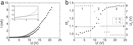
Figure 4. (a) Selected I(V) curves, inset—the beginning of an I(V) curve with linear approximation line for determination of U0; (b) relative change of the resonance frequency of the nanowire and characteristic voltage U0 versus maximum cycling voltage U'.
Download figure:
Standard image High-resolution imageIt was observed that the value of U0 decreases with the increase of the voltage U' applied to the nanowire during the experiment (figures 4(a) and (b)). As it is seen from figure 4(b), the beginning of the U0 decrease coincides with the beginning of rapid frequency increase. When the U0 decrease stops, the frequency increase stops as well.
This observation, as well as the fact that for all experiments (table 1) the frequency increase was strictly within 45%, lets us presume that all modification took place in contact as the increase of frequency represents increase of adhesion forces in contact. The change of U0 may be associated with reduction of effective oxide layer thickness and/or changes in native oxide layer conductive properties. As the current densities associated with welding of material and change in its structure in nanocontacts [31, 32] are two orders of magnitude higher than the saturation current density jst in our experiments, we can consider that conductive properties of native oxide layer do not change and therefore changes in U0 can be associated with decrease of distance between electrodes and increase of effective contact area. Increase of effective contact area may be the main reason for increase of adhesion force in a nanocontact.
In our configuration, electric contact consisted of Ge/native oxide/gold junction. The native oxide thickness was within range from 1 nm up to 3 nm (figure 5). We propose that for voltages used in our experiment the dominant mechanism of conductance is the Fowler–Nordheim (FN) tunneling, as reported for Ge-GeO2-Al and Si-SiO2/Au thin films of similar oxide thicknesses [41, 42]. Because of the nonlinearity of I(V) characteristics and presence of a 'nonconductive gap', in this evaluation we do not take into account quantum mechanical direct tunneling (QMDT), as its contribution to total current flow is negligible.
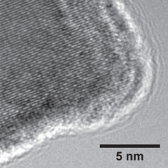
Figure 5. TEM micrograph of crystalline Ge nanowire with amorphous native oxide layer.
Download figure:
Standard image High-resolution imageFor evaluation of change of oxide layer thickness d during the experiment, the FN tunneling equation [41–43] was used: 
 where
where 
 q is an electron charge, m0 and mox are the electron mass in free space and in the oxide respectively, h is Planck's constant, ф0 is barrier height between native oxide, and Ge,
  is electric field, ox is dielectric permittivity of the oxide, and d is oxide layer thickness [41–43]. For calculations ф0 = 1.4 eV, ox = 2.72, mox = 0.42 m0 were used [41]. Results show that a small change in oxide layer thickness d induces a large change in U0. For example, the change in U0 from 7 to 3 V is achieved by decrease of an oxide layer thickness of approximately 0.1 nm assuming that the contact area is not changing. If d is kept at constant value, the same change in U0 may be achieved by triplication of effective contact area.
The process of switch contact strengthening can be divided in three stages. In the first stage, the electric current does not flow through the switch contact and the changes in it are negligible (figure 4(b) area 1). In the second stage (figure 4(b) area 2), the FN tunneling causes the current flow as well as Joule heating in the switch contact. We assume that at this stage Joule heating in the switch contact [37] causes modification of the Ge–native oxide–Au interface, which results in contact strengthening. During the modification, it can be presumed that the contacting surfaces of the nanowire and the switch electrode become flatter, i.e., smoothening out the contact roughness and increasing the effective Ge–native oxide–Au contact area as well as decreasing the distance between Ge core and gold electrode. At the stabilization point (figure 4(b) area 3), the effective contact area increases to a value at which the temperature in the contact area caused by the Joule heating is not high enough to continue the modification of the switch contact interfaces. According to the mechanical model, the switch contact is close to the 'fixed' state case (figure 4(b) area 3). Most probably, such modification is possible because at larger distances from Ge core surface, the native oxide is less dense than in inner layers (figure 5).
To determine how the changes of the contact's mechanical and electrical properties are influenced by the thickness of an oxide layer, measurements were carried out in different places on as grown and gradually etched Ge nanowire. Initial 'nonconductive' gap U0max for this nanowire varied from 8 to 3 V (figure 6). For nanocontacts exhibiting larger U0max larger maximum frequency increase ratios fmax/f0 and ΔU0 (ΔU0 = U0max-U0min, where U0min—characteristic voltage after frequency stabilization) were observed (figure 6). It can be explained that for larger U0max the outer and less dense oxide layer is thicker and can be modified more effectively. Accordingly, for smaller values of U0max, the oxide layer is thinner and more dense; therefore, modification of the surface is less pronounced and thus changes in 'nonconductive gap' ΔU0 and adhesion force are smaller.
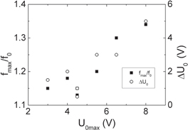
Figure 6. Maximum frequency increase ratio and maximum change of U0 (ΔU0) versus initial 'nonconductive gap' U0max.
Download figure:
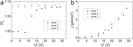
Standard image High-resolution imageTo determine the stability of contact modifications, three consequent measurement cycles without disengaging the switch contact for the nanowire in its ON state were performed (figure 7(a)). It can be seen that once the rapid increase of the resonance frequency had occurred (figure 7(a) cycle 1), repeated voltage application (figure 7(a) cycles 2, 3) did not result in additional increase of resonance frequency. This also indicates no further changes in mechanical properties of the contact. The graph of current density versus applied voltage (figure 7(b)) shows that conductivity of the contact increases slightly during cycle 1 and remains stable during cycles 2 and 3. This suggests that, for a fixed voltage range, the electrical properties of the contact do not change with further cycling.
Figure 7. (a) Relative change of the resonance frequency of the nanowire versus maximum applied voltage U' for consequent voltage cycles without disengaging the contact; (b) current density in the contact versus maximum applied voltage U' for consequent voltage cycles without disengaging the contact.
Download figure:
Standard image High-resolution image
4. Conclusions
In this work, we have presented an application of resonance frequency measurements for characterization of the NEM switch contact modification during its operation in the ON state. This novel method allows an indirect evaluation of adhesion forces in contact without detachment of the nanowire. The main problem for adhesion force measurements using nanowire detachment from the surface is the parasitic shear forces that lower the effective pull-out force, thus inducing error in measurements. The knowledge about the change in contact parameters during operation of the NEM switch is of great importance to evaluate the stability of NEM switch operation.
We found that the switch contact strengthening begins simultaneously with the start of electric current flow through it and stops at current densities of 10−3 − 10−2 nA nm−2. The magnitude of change of the resonance frequency has strong positive dependence on the initial characteristic voltage ('nonconductive gap') U0 of the nanowire as it represents the initial oxide thickness (amount of the material in the contact) and its structure. For thick oxide layers, the outer shells are less dense than the inner layers, thus less resistant to current induced deformation, which in comparison to thinner oxides leads to bigger voltage/current-induced changes of its thickness. We also demonstrated that strengthening of the switch contact is permanent for given voltage/current density ranges.
Acknowledgments
The study has been supported by the Latvian Council of Science.