
Abstract
The structural and optical properties of GaAs1−xBix quantum wells (QWs) symmetrically clad by GaAs barriers with and without additional confining AlGaAs layers are studied. It is shown that a GaAs/GaAs1−xBix/GaAs QW with x ∼ 4% and well width of ∼4 nm grown by molecular beam epitaxy demonstrates efficient photoluminescence (PL) that becomes significantly more thermally stable when a cladding AlGaAs layer is added to the QW structure. The PL behavior for temperatures between 10 and 300 K and for excitation intensities varying by seven orders of magnitude can be well described in terms of the dynamics of excitons including carrier capture in the QW layer, thermal emission and diffusion into the cladding barriers. Understanding the role of these processes in the luminescence of dilute GaAs1−xBix QW structures facilitates the creation of highly efficient devices with reduced thermal sensitivity and low threshold current.
Export citation and abstract BibTeX RIS
1. Introduction
Recent progress in the controlled growth of low dimensional semiconductor systems has allowed for precise band structure engineering of new materials with potential uses in modern electronic and photonic applications [1–3]. The replacement of a small amount of arsenic by bismuth during the molecular beam epitaxy (MBE) of GaAs based nanostructures has produced GaAs1−xBix layers with unusual electronic properties [4–6]. Experimental investigations of these dilute bismide alloys have revealed a bandgap energy, Eg(x), which is surprisingly insensitive to changes in temperature and which shifts to lower energies quickly at a rate of up to ∼90 meV/% of incorporated Bi. Similarly, the spin–orbit-splitting energy, ΔSO, has been found to have a large upward bowing component, and for alloys with x > 0.1 [7] ΔSO becomes larger than Eg. This becomes important for suppression of Auger recombination in alloys with high Bi composition having emission wavelengths in the 1.3–1.5 μm telecommunication band. There are efforts to resolve the challenges of controlling the low temperature epitaxial growth which is required for the incorporation of a significant molar percentage of Bi into GaAs [8–10] as well as for growing high quality device components [11–13]. However, to be able to investigate the structural and electronic properties, the nature of defects, the emission channels and the efficiency of carrier recombination in these structures in order to develop further recommendations for controlled growth, redesign and optimization in the continuous search for new device elements based on dilute bismide alloys is required [14–18].
In a recent paper [10], we reported the MBE growth of GaAs/GaAsBi/GaAs heterostructures clad by AlGaAs confinement barriers which demonstrated excellent structural properties. In spite of the low temperature growth regime, we were able to obtain high quality AlGaAs cladding layers. These structures are good candidates for the realization of room temperature continuous-wave electrically pumped laser diodes. In this work we present the results of a comprehensive study of the structural and optical properties of GaAs/GaAsBi/GaAs heterostructures after comparison between measurements in samples with and without additional confining AlGaAs cladding layers. We analyze the influence of the additional symmetric spatial confinement induced by the AlGaAs layers on the optical emission from electronic states in the GaAs1−xBix quantum well (QW).
2. Characterization of samples
Two single sets of GaAsBi QW samples were grown on semi-insulating GaAs(001) substrates using a Riber-32P MBE system. Sample A consisted of purely GaAs barriers and sample B consisted of additional Al0.3Ga0.7As barriers at the edge of the GaAs offsets both above and below the GaAsBi QW. In order to produce sample B it was necessary to use an asymmetric temperature profile during growth. The bottom AlGaAs barrier was grown at an optimal temperature of 610 ° C, while due to the low optimal growth temperature for GaAsBi the QW layer and the top AlGaAs barrier were grown at 320 ° C. In order to grow the entire structure without interruption following the drop in substrate temperature, while creating a stoichiometric growth condition for the GaAsBi QW, the As to Ga flux ratio was set to unity following the first AlGaAs barrier. This condition was maintained through the growth of the QW, after which the As flux was quickly increased, without interruption in the growth, until an As to Ga flux ratio of 2.4 was achieved so that any remaining Bi on the surface would be displaced and not incorporate into the growth. As we will demonstrate below, this was only partially successful. This flux ratio was maintained throughout the rest of the growth, and the second AlGaAs barrier was grown by simply introducing Al at a 3:7 ratio to the Ga flux. Further growth details are given in [10].
Sample characterization was performed by means of transmission electron microscopy (TEM) and high-resolution x-ray diffraction (HR-XRD). For the cross-sectional TEM measurements, the samples were prepared using mechanical polishing followed by ion-milling in a Fischione 1010 ion mill. The TEM observations were performed at 300 keV in an FEI Titan 80–300 S TEM fitted with a CEOS image corrector. Figures 1(a) and (b) display the bright-field images obtained under two-beam conditions with the (002) reflecting planes in samples A and B, respectively. Here the substrates are located on the left side of both images. The GaAsBi layer appears darker between the lighter layers in both samples, whereas the AlGaAs cladding layers are brighter in sample B. The darker band appearing at the AlGaAs–GaAs interface on the left side is most likely a result of surface contamination during the long growth interruption in which the temperature was lowered during this stage of the growth process [10]. It is seen that the thicknesses of the GaAsBi layer is 4.1 ± 0.6 nm in sample A and 5.0 ± 0.6 nm in sample B (see table 1) without any remarkable thickness variations along the entire length of the sample. The interface of each layer is smooth and very well-defined with transition regions of only 1–2 monolayers (ML). Also, the lateral Bi distribution within the GaAsBi layers appears to be quite homogeneous and, within the uncertainty introduced by sample preparation artifacts, we find no noticeable fluctuations in the Bi concentration in the plane of the layer. However, the out of plane XRD simulations show a stepped Bi concentration gradient, which is again uniform within the plane, as shown in figures 1(c) and (d). This will be discussed further below. The high quality of the low temperature AlyGa1−yAs barrier, seen on the right in figure 1(d), is attributed to the surfactant properties of residual Bi on the surface. Its presence is indicated by a (1 × 3) surface reconstruction persisting throughout the low temperature growth. The thicknesses of the AlyGa1−yAs barriers are 14.5 ± 0.7 nm for the high temperature layer on the left and 11.1 ± 0.6 nm for the low temperature layer on the right. Furthermore, the x-ray measurements show GaAsBi layers with very good crystalline structures.
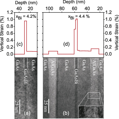
Figure 1. Bright-field TEM images measured under two-beam conditions with (002) reflecting planes in (a) sample A and (b) sample B. The GaAsBi layer is seen as a dark contrast between the gray GaAs layers. The AlGaAs cladding layers appear as brighter bands in (b). In both panels (a) and (b) the substrate is to the left and the surface to the right of the images. Corresponding vertical strain profiles as derived from x-ray simulations for (c) sample A and (d) sample B are shown on the top.
Download figure:
Standard image High-resolution imageTable 1. Experimental results for the maximum Bi content, xmax, and thicknesses, dQW, of the GaAsBi QWs as determined by HR-XRD and TEM.
| Sample | xmax (%) | dQW (nm) | |
|---|---|---|---|
| HR-XRD | HR-XRD | TEM | |
| A | 4.2 ± 0.2 | 3.9 ± 0.5 | 4.1 ± 0.6 |
| B | 4.4 ± 0.6 | 4.4 ± 0.8 | 5.0 ± 0.6 |
In the HR-XRD analysis, reciprocal space mappings were performed in the vicinity of the asymmetric (224) Bragg reflection for sample A, as shown in figure 2(b), and for sample B, as shown in figure 2(c). These mappings demonstrate that all layers are pseudomorphically (coherently) strained in both samples. In addition, the pronounced thickness fringes along the narrow (224) crystal truncation rods (CTR) and the absence of diffuse scattering in the vicinity of the CTRs indicate smooth interfaces and a low density of defects for both samples. The corresponding experimental high-resolution x-ray rocking curves (2θ − ω) of the symmetric (004) Bragg reflections are presented in figure 2(a) for both samples. Again, the pronounced thickness fringes observed demonstrate the high quality and the long-range coherence of both samples. The x-ray simulations were carried out in the framework of a quasi-kinematical scattering algorithm [14] that allows a quantitative analysis of the experimental rocking curves. By applying a least-square fitting procedure to the x-ray simulations, the vertical distribution of Bi inside the GaAs1−xBix QWs, the corresponding vertical strain distribution and the GaAs1−xBix layer thicknesses were determined with high accuracy. It appears, however, that the experimental rocking curves cannot be fitted with sufficient accuracy by using only a single GaAs1−xBix layer with a uniform Bi concentration x. For this reason we constructed a model which uses multiple fitting layers indexed with i having different Bi concentrations and widths (xi and di), thus replacing the GaAs1−xBix film of the nominal width. The results for the vertical strain profiles are shown in figures 1(c) and (d) by solid lines where they can be compared with the corresponding TEM images. By using the parameters of these constituents derived from the best fit, an effective QW layer thickness dQW can be defined by

where xmax is the maximum Bi concentration in the GaAsBi QW. These QW parameters are presented in table 1 where a comparison with the thicknesses determined from TEM can be made. It can be seen here that the maximum Bi concentration and width of the GaAsBi QW are fairly close in both structures, which makes their comparison with respect to the addition of the AlGaAs cladding more representative. However, the uncertainty in the values for sample B is slightly larger due to the larger number of fitting parameters. The simulations are insensitive to the GaAs buffer layer; however, they do show that the GaAs and AlGaAs layers grown after the GaAsBi QW are slightly strained vertically. This is most likely due to incorporation of residual Bi into the growth after the completion of the QW. It was observed that Bi which did not incorporate into the QW structure remained on the surface of the substrate throughout the rest of the low temperature growth process. This excess Bi evidently incorporated into the growth of the capping layers, resulting in the observed strain without any other significant effects. However, the results of both TEM and HR-XRD analysis are very close (see figure 1) and indicate samples with high structural quality. In particular, the thicknesses obtained by HR-XRD for the bottom (14.3 ± 0.5 nm) and top (12.0 ± 0.5 nm) AlGaAs barriers are in very good agreement with the TEM estimates. The GaAs1−xBix layers are both found to have concentrations of x ∼ 4%, and thicknesses of dQW ∼ 4 nm (table 1). We will now see how these thin GaAs1−xBix layers symmetrically clad by GaAs barriers with and without the additional symmetric confinement by AlGaAs layers develop through exciton photoluminescence (PL).
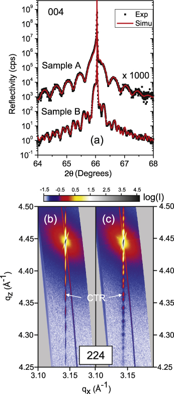
Figure 2. (a) Experimental x-ray rocking curves (symbols) around the GaAs(004) symmetrical Bragg reflection for samples A and B plotted together with corresponding simulations (solid red lines). Reciprocal space mappings for (b) sample A and (c) sample B in the vicinity of the 224 reciprocal lattice point of GaAs.
Download figure:
Standard image High-resolution image3. PL measurements: results and discussions
PL measurements were performed using a range of excitation intensities and temperatures. The samples were mounted in a variable temperature, 10–300 K, closed-cycle helium cryostat and the PL emission was excited by the 532 nm line of a frequency doubled Nd:YAG laser. The laser beam with power in the range of ∼(10−6–102) mW was focused to a spot having a diameter of ∼20 μm. The PL signal was dispersed by a 0.5-m single-grating monochromator and detected by a liquid nitrogen (LN)-cooled OMA V: InGaAs photodiode detector array.
3.1. Excitation power dependence
Figure 3 shows the low temperature, T = 15 K, PL spectra of sample A (figure 3(a)) and sample B (figure 3(b)) measured with excitation intensities Iex ranging from 3.7 × 10⁻⁴ to 1.0 × 10⁴ W cm−2. The low energy PL band near 1.150 eV in each sample is assigned to emission from the GaAsBi QW layers, whereas the high energy peak near 1.510 eV is assigned to bulk-like GaAs exciton emission, under strain. By increasing Iex from 3.7 × 10⁻⁴ to 1.0 × 10⁴ W cm−2, the maxima of the QW PL bands, Emax, undergo a blue-shift from 1.177 to 1.242 eV in sample A and from 1.202 to 1.253 eV in the AlGaAs clad sample. The small difference in the low power QW exciton energies between samples A and B (∼25 meV) is attributed to the slightly lower Bi concentration (∼0.3%) found in sample B, (see table 1). To analyze the QW emission from the two samples we plot the energy of the PL maxima in figure 4(a), the full width at half maximum (FWHM) of the PL peaks in figure 4(b) and the integrated PL intensity in figure 4(c), as functions of the excitation power for both samples A and B. Generally speaking the behavior of the PL band parameters can be interpreted in terms of competing radiative and nonradiative channels for free and localized excitons as has been widely discussed for dilute bismides and nitrides [14, 19–21]. In order to identify these channels we examine the QW PL line shape more closely. Figure 5(a) displays the PL spectrum of sample A, measured at low temperature, T = 15 K, and low excitation power, Iex = 6.0 mW cm−2. The spectrum is noticeably broadened towards the lower energy side. The origin of the observed asymmetry is a low energy PL band,  , revealed by fitting the spectrum with two Gaussians. This comparatively broad PL band is red-shifted by ∼60 meV with respect to the high energy PL band,
  , which has a significantly smaller FWHM. These two constituents are present in all measured spectra of samples A and B but the ratio between their maximal intensities depends on Iex. At high excitation intensities the
  band dominates the PL spectrum. The
  band appears to saturate, indicating the finite density of states from which it emits. These two basic PL contributions are attributed to emission of QW excitons,
  , and bound-excitons,
  , localized by defects and disorder in the bismide QW [6, 15]. Competition of QW excitons and bound-excitons in different ranges of Iex defines the PL line shape and the behavior of the PL band parameters shown in figure 4. The linear dependence of the integrated PL intensity (figure 4(c)) reflects a dominant contribution of radiative excitonic transitions in the PL spectra in the region between weak to moderate excitation power densities (Iex ∼ 1 W cm−2). This excitonic recombination is usually wider in sample B, if compared to sample A, due to additional channels of PL excitation supplied by the AlGaAs cladding layers.
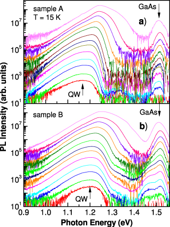
Figure 3. Low temperature (T = 15 K) PL spectra measured at different power excitation intensities, Iex, from 3.7 × 10⁻⁴ W cm−2 (red spectra on the bottom) to 1.0 × 10⁴ W cm−2 (pink spectra on the top) in (a) sample A and (b) sample B. Note the blue-shift and change in the lineshape induced by increasing power excitation.
Download figure:
Standard image High-resolution image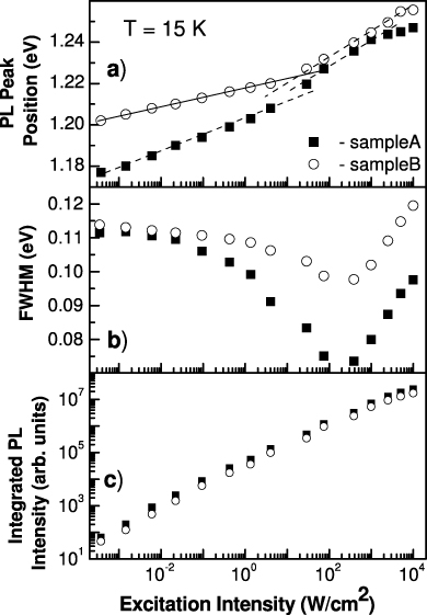
Figure 4. Dependences of the QW PL band parameters on the power excitation intensity for samples A (filled squares) and B (open circles) as derived from the spectra shown in figure 3: (a) the energy of the PL maximum, (b) FWHM and (c) integrated PL intensity.
Download figure:
Standard image High-resolution image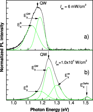
Figure 5. Low temperature (T = 15 K) PL spectra measured at (a) Iex = 6 mW cm−2 and (b) Iex = 1 × 10⁴ W cm−2 in sample A. The Gaussian fittings are shown in color.  ,
,  ,
,  and
and  stand for the QW exciton, bound-exciton, excited state exciton and bulk GaAs exciton emission energies, respectively.
Download figure:
Standard image High-resolution imageAs can be seen from figure 4 (Iex > 100 W cm−2) the behavior of the PL parameters at high excitation power changes in comparison with the weak excitation power regime for both samples. The reason for this change becomes clear from figure 5(b) where the low temperature PL spectrum, measured at Iex = 1.0 × 10⁴ W cm−2, is shown. Besides the bulk-like GaAs edge emission we can distinguish clearly a new PL contribution,  , above the dominant
  emission in the QW PL spectrum. This new PL band, blue-shifted ∼50 meV from the
  peak energy, is attributed to the QW excited state seen previously as a significantly narrower PL emission (FWHM ∼ 40 meV) from the GaAsBi QW [14]. It is worth noticing here that we observe only one excited state (n = 1) in the QWs under investigation, whereas in the samples studied in [14] the state with n = 2 in the conduction band could be observed for high excitation intensity PL spectra. The difference is that in the recent studies the QWs are significantly narrower (dQW ∼ 4 nm) than that investigated in [14] with dQW ∼ 12 nm, and the state with n = 2 is unbound. The increasing intensity of the
  band leads to a further blue-shift of the QW PL maximum and to a significant high energy asymmetry of the lineshape. At the same time, an increased excitation power results in the saturation of the
  emission due to the limited number of localized states, as can be seen in figures 5(a) and (b). Due to a higher density of excitons inside the QW at high Iex, nonradiative recombination becomes favorable and thus reduces the number of excitons which can recombine radiatively leading to the sub-linear power excitation dependence,
  , as shown in figure 4(c).
3.2. Temperature dependence
The PL spectra of samples A and B, taken with Iex = 0.4 W cm−2 for temperatures between 15 and 300 K, are shown in figures 6(a) and (b), respectively. It is clearly seen that the PL spectra shift towards low energies with increasing temperature in both samples, accompanied by substantial changes of the QW PL lineshape. Here, the QW PL maxima first red-shift as the temperature increases, then reverse and blue-shift at a characteristic temperature which is different for each sample. These behaviors are summarized in figure 7(a) and the corresponding changes in the FWHM are presented in figure 7(b). The dependence of the PL peak energy and the FWHM are attributed to the different behaviors of the two PL constituents, i.e. the broad PL emission from bound-excitons,  , and the narrower QW exciton emission,
  , which were discussed in figure 5(a) and are detected at all temperatures from both samples. The QW exciton emission rapidly decays as compared to the bound-exciton decay as the temperature increases. As a result, the ratio between the maxima of the
  and
and  peaks strongly depends on temperature leaving the
  emission dominant for higher temperatures up to ∼170 K in sample A and ∼200 K in sample B. Below these characteristic temperatures the PL peaks broaden and red-shift towards
  followed by a transition to blue-shifting of the emission.

Figure 6. PL spectra of samples A (a) and B (b) measured at Iex = 0.4 W cm−2 for the temperature range between 15 and 300 K. Above T = 20 K the temperature increases in steps of 10 K.
Download figure:
Standard image High-resolution image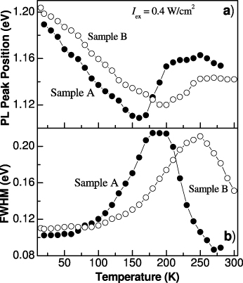
Figure 7. Temperature dependences of the QW PL band measured at Iex = 0.4 W cm−2 in samples A (filled symbols) and B (open symbols): (a) the energy of the PL maximum, (b) the FWHM.
Download figure:
Standard image High-resolution imageThe origin of the S-shaped temperature dependence of the PL peak position shown in figure 7(a) is well documented (see, for example, [14, 15]) and recently refined [22, 23]. Let us analyze the PL line shape (figure 6) at higher temperatures using multiple Gaussians. The fitting for sample A, for T = 170 K and Iex = 0.4 W cm−2, is shown in figure 8 and reveals the additional band, on the high energy side of the QW peak. This coincides with the QW exciton excited state transition,  , found at ∼50 meV above the
  peak for the high power regime of both samples in figure 5(b). As a result, we attribute the blue-shift of the PL band at high temperatures to thermal pumping of the QW excited exciton,
  , state with simultaneous decay from the bound,
  , and the QW,
  , excitons. Emission from these three states results in the maxima seen in the FWHM curves in figure 7(b). Subsequent narrowing of the PL band for higher temperatures is related to the rapid temperature decay of high energy excitation and energy transfer to low lying energy states. Such a situation is typical for dense quantum dot ensembles [24]. As a result the high temperature FWHM value can be smaller than the low temperature one, as seen in figure 7(b).
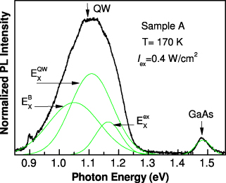
Figure 8. The PL spectrum measured at Iex = 0.4 W cm−2 and T = 170 K for sample A. The Gaussian fittings are shown in color.  ,
,  and
and  stand for the QW exciton, bound-exciton and excited state exciton energies, respectively.
Download figure:
Standard image High-resolution imageWe therefore conclude that the character and lineshape of the PL spectrum is dependent on the relative strengths of the  ,
,  and
and  excitonic emissions which are strongly dependent on both temperature T and excitation intensity Iex. Therefore, combining these two parameters (T and Iex) we can tailor different functional dependences for the QW PL emission in these dilute bismide QW samples. Figure 9 shows the energy of the PL maxima and the FWHMs in our samples as a function of temperature, measured at high excitation power, Iex = 75 W cm−2. Because the free excitonic contributions,
  and
and  , dominate, even at high temperatures, the deep minimum near T = 170 K, as seen in figure 7(a) for low power excitation, disappears. The decrease of the energy of the PL maximum resembles the temperature dependence of the bulk GaAs energy gap,
  , more closely, as shown in figure 9(a). The changes in the FWHM with increasing temperature are shown in figure 9(b) for the QW and GaAs emissions. Note that the temperature dependence of the
  transition in sample A follows closely the
  dependence above 170 K. The solid line is the calculated
  values according to the Varshni law [25], as
with E0 = 1.516 eV, α = 8.95 × 10⁻⁴ and β = 600 K. This set of fitting parameters is very similar to the values reported in [26–28]. The different behavior of the energy of the PL maximum and FWHM in sample A and sample B can be attributed to the presence of the excited state transition, which in sample B maintains much of its low temperature emission intensity due to the presence of the AlGaAs confinement layers. The additional confinement in sample B effectively reduces the loss resulting from the thermal excitation of carriers out of the QW system which is observed in sample A at elevated temperature. This forces the system in sample B to act very similarly in both low and high pump power regimes as a function of temperature, whereas sample A exhibits a dramatic loss of excitation, for high pump power, when the temperature becomes sufficient to excite the carriers which are populating the excited state back into the GaAs where they are subsequently lost from the QW. This conclusion is supported further by the results of section 4.
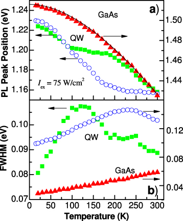
Figure 9. Temperature dependences of the QW PL band parameters measured at Iex = 75 W cm−2 in sample A (filled symbols) and sample B (open symbols). (a) The energy of the PL maximum and (b) the FWHM. The temperature dependences of the GaAs bandgap energy, Eg(T), in (a) and the FWHM of the GaAs PL band in (b) are shown by triangles. Fitting using the Varshni law (see equation (2)) is shown as a solid line in (a).
Download figure:
Standard image High-resolution image4. Dynamics of excitons in the bismide structures
The additional confinement introduced by the symmetric AlGaAs cladding layers strongly influences the recombination processes in the GaAsBi QW. We have observed that the spectral features of the QW containing the additional AlGaAs cladding layers (sample B) are wider than for the isolated GaAs/GaAsBi/GaAs QW (sample A) for all values of Iex (see figure 4(b)). In order to explore this observation more deeply we apply a rate model to describe the carrier relaxation in the QW sample with the AlGaAs cladding. The model is based on rate equations for the intrawell relaxation [22, 23] along with a set of continuity equations that takes into account the density of excitons in the bulk GaAs, nB and in the bismide quantum well, nQW and the exciton current density, j, as proposed by Bacher [29].
To describe intrawell exciton dynamics we use the following parameters for the QW excitons: density, nQW; energy,  ; decay rate,
  , where
  and
and  are the times of radiative and nonradiative exciton recombination, respectively. The QW contained, impurity-bound excitons have energy
  and decay rate
  , where τri and τnri are the times of radiative and nonradiative bound-exciton recombination, respectively; and density, ni. Here, i represents the ith impurity site with finite density of states, Ni. A QW exciton can be trapped by an impurity site at rate, τcpl-1, creating a bound-exciton. Similarly, a bound-exciton can be thermally released, becoming a QW exciton at a rate of τth-1.
In order to complete the model we have to take into account contributions from transport, reflection, transmission and capture of excitons in the GaAs barrier to the dynamics of QW excitons. By introducing the density of excitons in the GaAs bulk, nB, and the exciton current density, j, we can create a set of continuity equations for the density of excitons in the bulk, in the QW and bound to impurities as

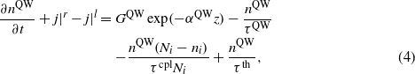

To these, we add Fick's law for the exciton current density j,
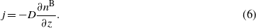
In these equations, j|l and j|r stand for the exciton current density from the left and right borders of the QW, D is the diffusion coefficient and G, α and τ are the generation rates, absorption coefficients and lifetimes in the bulk, QW or impurity according to the superscripts B, QW or cpl, respectively. It is further assumed that light is entering the sample perpendicular to the system at z = 0 and all the dynamics is essentially one-dimensional due to highly uniform layers in samples A and B, thus any contribution from transport parallel to interfaces may be neglected.
The excitons moving in the GaAs barrier reach the QW area where they can be transmitted, reflected or trapped. The sums of these probabilities are normalized to one. Following [29] we introduce the thermal exciton transmission, st, and capture, sc, velocities which are multiplied by the corresponding transmission and capture probabilities defining the current of excitons in the left and right GaAs layers as


where the probability for thermal emission out of the QW has a time rate of (τout)−1. Here, the capture rate of an exciton into the well and the emission rate out of the well are modeled by scattering with an optical phonon, as in [29], and are given by sc and (τout)−1. In addition, the interfaces of the AlyGa1−yAs cladding layers, the surface of the sample and the interface with the substrate are treated as boundaries with st = 0, i.e. the probability for an exciton to transmit or escape through these boundaries is zero. The exciton capture and emission at these interfaces are considered as free fitting parameters. The set of rate equations (equations (3)–(5)) can the be solved under steady state conditions by setting ∂nB/∂t = 0, ∂nQW/∂t = 0, and ∂ni/∂t = 0 resulting in

and

Here we have set  ,
,  , and
, and  . One can see that nQW is proportional to τQW for low temperatures if we assume that (τout)−1 → 0. Also, we have
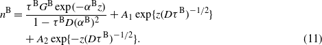
The coefficients Ai can be easily obtained by solving a matrix equation. Taking into account that the PL intensity is described in terms of the exciton density, one has  and
and  for the QW and bound-exciton emissions, respectively. C is a factor which depends on the actual experimental arrangement but is (essentially) identical for both QW and bound-excitons. Finally, the expression for the total emission intensity,

can be used for the analysis of experimental data.
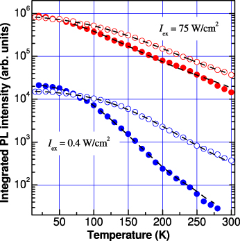
Solutions (9)–(12) allow for the investigation of the influence of the cladding layers on the character of the PL emission from the GaAsBi QW. It follows from these expressions that QW PL gain would be determined by an efficient generation rate,  , that includes an additional term, sc(nB|l+nB|r), depending on the strength of the reflection or capture at the interfaces. The contribution from reflection influences the exciton distribution both in the GaAs barrier and in the GaAsBi QW. As a result, the efficiency of excitation of different states in the QW and bound states increases. In the case of completely absorbing AlGaAs barriers, the excitons leave the QW at high temperatures decreasing the density of excitons and quenching the PL. In the other extreme case of completely reflecting barriers, excitons thermally emitted from the QW move towards the AlGaAs barrier, reflect and return to be re-absorbed by the QW, thus leading to stronger PL. For intermediate cases it is clear that the density of excitons, and thus the intensity of emission at high temperatures, will be defined by the character of the AlGaAs barrier. Figure 10 shows the temperature dependence of the integrated QW PL intensities measured in samples A and B at two different excitation powers. Let us compare the results of a calculation using the set of equations (9)–(12) and our experimental results. For the simulation we calculated the temperature dependences of sc(T) and (τout(T))−1 using the formulae (A1) and (A2) in [29]. The diffusion coefficient was taken from [30], and the absorption coefficient was taken from the literature. The time constants for carrier relaxation were taken from [14, 23, 29, 31]. Thus, only the interface parameters are used to fit the experiments. The results of this simulation are shown in figure 10 by the dashed lines. It is clearly seen that the model proposed for the description of the exciton dynamics in the case of increasing temperature within a cladding barrier works quite well. This model explains the enhanced thermal stability of the QW emission for the case of the additional confinement induced by an AlGaAs cladding layer due to re-absorption of excitons thermally emitted from the QW and recaptured after reflection from the barriers in the area of the QW. In fact the reflecting cladding layer effectively reduces the carrier loss due to nonradiative recombination in the GaAs barrier.
Figure 10. Temperature dependences of the integrated PL intensities measured in samples A (filled symbols) and B (open symbols) at two different excitation intensities, Iex = 0.4 W cm−2 and Iex = 75 W cm−2. A good agreement obtained from simulations using the set of equations (9)–(12) is shown by the dashed lines for the total intensity obtained from equation (12).
Download figure:
Standard image High-resolution image
5. Final comments and conclusions
We have studied the structural and optical properties of a GaAs1−xBix quantum well (QW) clad by a GaAs barrier with and without the additional confinement of AlGaAs cladding barriers. It is shown that a GaAs/GaAs1−xBix/GaAs QW with a Bi concentration of ∼4% and well width of ∼4 nm grown by molecular beam epitaxy exhibits efficient photoluminescence. The growth of additional AlGaAs cladding layers induces a significant increasing in the thermal stability of these bismide QW structures. The dependence of the PL on temperature and excitation intensity is well described in terms of exciton dynamics including carrier capture in the QW and thermal emission and diffusion in the GaAs barriers. A dynamical model for the exciton rate equations explains the enhanced thermal stability of QW emission in samples with and without the additional AlGaAs confinement. This model includes re-absorption of excitons thermally emitted from the QW and returned after reflecting from barriers in the area of the QW. In fact, reflection effectively reduces the carrier loss due to nonradiative recombination in the GaAs barrier thus significantly influencing the recombination processes in additionally confined structures. Understanding of these processes in dilute GaAs1−xBix QW structures shows a robust path to the creation of highly efficient devices with reduced loss and are good candidates for the realization of room temperature continuous-wave electrically pumped laser diodes.
Acknowledgments
The authors acknowledge the financial support by the US National Science Foundation (NSF) via grant no. DMR-0520550 and MWN (Material World Network) Program between the NSF (grant no. DMR-1008107) and the Deutsche Forschungsgemeinschaft (grant no. Li 580/8-1). S-Q Yu acknowledges support by NSF Career Award no DMR-1149605.